EP0346055A2 - Procédé pour provoquer une réaction dans le plasma sous pression atmosphérique - Google Patents
Procédé pour provoquer une réaction dans le plasma sous pression atmosphérique Download PDFInfo
- Publication number
- EP0346055A2 EP0346055A2 EP89305671A EP89305671A EP0346055A2 EP 0346055 A2 EP0346055 A2 EP 0346055A2 EP 89305671 A EP89305671 A EP 89305671A EP 89305671 A EP89305671 A EP 89305671A EP 0346055 A2 EP0346055 A2 EP 0346055A2
- Authority
- EP
- European Patent Office
- Prior art keywords
- substrate
- atmospheric pressure
- plasma
- gas
- reaction
- Prior art date
- Legal status (The legal status is an assumption and is not a legal conclusion. Google has not performed a legal analysis and makes no representation as to the accuracy of the status listed.)
- Granted
Links
Images



Classifications
-
- C—CHEMISTRY; METALLURGY
- C23—COATING METALLIC MATERIAL; COATING MATERIAL WITH METALLIC MATERIAL; CHEMICAL SURFACE TREATMENT; DIFFUSION TREATMENT OF METALLIC MATERIAL; COATING BY VACUUM EVAPORATION, BY SPUTTERING, BY ION IMPLANTATION OR BY CHEMICAL VAPOUR DEPOSITION, IN GENERAL; INHIBITING CORROSION OF METALLIC MATERIAL OR INCRUSTATION IN GENERAL
- C23C—COATING METALLIC MATERIAL; COATING MATERIAL WITH METALLIC MATERIAL; SURFACE TREATMENT OF METALLIC MATERIAL BY DIFFUSION INTO THE SURFACE, BY CHEMICAL CONVERSION OR SUBSTITUTION; COATING BY VACUUM EVAPORATION, BY SPUTTERING, BY ION IMPLANTATION OR BY CHEMICAL VAPOUR DEPOSITION, IN GENERAL
- C23C16/00—Chemical coating by decomposition of gaseous compounds, without leaving reaction products of surface material in the coating, i.e. chemical vapour deposition [CVD] processes
- C23C16/44—Chemical coating by decomposition of gaseous compounds, without leaving reaction products of surface material in the coating, i.e. chemical vapour deposition [CVD] processes characterised by the method of coating
- C23C16/455—Chemical coating by decomposition of gaseous compounds, without leaving reaction products of surface material in the coating, i.e. chemical vapour deposition [CVD] processes characterised by the method of coating characterised by the method used for introducing gases into reaction chamber or for modifying gas flows in reaction chamber
- C23C16/45563—Gas nozzles
- C23C16/4558—Perforated rings
-
- C—CHEMISTRY; METALLURGY
- C23—COATING METALLIC MATERIAL; COATING MATERIAL WITH METALLIC MATERIAL; CHEMICAL SURFACE TREATMENT; DIFFUSION TREATMENT OF METALLIC MATERIAL; COATING BY VACUUM EVAPORATION, BY SPUTTERING, BY ION IMPLANTATION OR BY CHEMICAL VAPOUR DEPOSITION, IN GENERAL; INHIBITING CORROSION OF METALLIC MATERIAL OR INCRUSTATION IN GENERAL
- C23C—COATING METALLIC MATERIAL; COATING MATERIAL WITH METALLIC MATERIAL; SURFACE TREATMENT OF METALLIC MATERIAL BY DIFFUSION INTO THE SURFACE, BY CHEMICAL CONVERSION OR SUBSTITUTION; COATING BY VACUUM EVAPORATION, BY SPUTTERING, BY ION IMPLANTATION OR BY CHEMICAL VAPOUR DEPOSITION, IN GENERAL
- C23C16/00—Chemical coating by decomposition of gaseous compounds, without leaving reaction products of surface material in the coating, i.e. chemical vapour deposition [CVD] processes
- C23C16/22—Chemical coating by decomposition of gaseous compounds, without leaving reaction products of surface material in the coating, i.e. chemical vapour deposition [CVD] processes characterised by the deposition of inorganic material, other than metallic material
- C23C16/30—Deposition of compounds, mixtures or solid solutions, e.g. borides, carbides, nitrides
-
- C—CHEMISTRY; METALLURGY
- C23—COATING METALLIC MATERIAL; COATING MATERIAL WITH METALLIC MATERIAL; CHEMICAL SURFACE TREATMENT; DIFFUSION TREATMENT OF METALLIC MATERIAL; COATING BY VACUUM EVAPORATION, BY SPUTTERING, BY ION IMPLANTATION OR BY CHEMICAL VAPOUR DEPOSITION, IN GENERAL; INHIBITING CORROSION OF METALLIC MATERIAL OR INCRUSTATION IN GENERAL
- C23C—COATING METALLIC MATERIAL; COATING MATERIAL WITH METALLIC MATERIAL; SURFACE TREATMENT OF METALLIC MATERIAL BY DIFFUSION INTO THE SURFACE, BY CHEMICAL CONVERSION OR SUBSTITUTION; COATING BY VACUUM EVAPORATION, BY SPUTTERING, BY ION IMPLANTATION OR BY CHEMICAL VAPOUR DEPOSITION, IN GENERAL
- C23C16/00—Chemical coating by decomposition of gaseous compounds, without leaving reaction products of surface material in the coating, i.e. chemical vapour deposition [CVD] processes
- C23C16/22—Chemical coating by decomposition of gaseous compounds, without leaving reaction products of surface material in the coating, i.e. chemical vapour deposition [CVD] processes characterised by the deposition of inorganic material, other than metallic material
- C23C16/30—Deposition of compounds, mixtures or solid solutions, e.g. borides, carbides, nitrides
- C23C16/34—Nitrides
- C23C16/345—Silicon nitride
-
- C—CHEMISTRY; METALLURGY
- C23—COATING METALLIC MATERIAL; COATING MATERIAL WITH METALLIC MATERIAL; CHEMICAL SURFACE TREATMENT; DIFFUSION TREATMENT OF METALLIC MATERIAL; COATING BY VACUUM EVAPORATION, BY SPUTTERING, BY ION IMPLANTATION OR BY CHEMICAL VAPOUR DEPOSITION, IN GENERAL; INHIBITING CORROSION OF METALLIC MATERIAL OR INCRUSTATION IN GENERAL
- C23C—COATING METALLIC MATERIAL; COATING MATERIAL WITH METALLIC MATERIAL; SURFACE TREATMENT OF METALLIC MATERIAL BY DIFFUSION INTO THE SURFACE, BY CHEMICAL CONVERSION OR SUBSTITUTION; COATING BY VACUUM EVAPORATION, BY SPUTTERING, BY ION IMPLANTATION OR BY CHEMICAL VAPOUR DEPOSITION, IN GENERAL
- C23C16/00—Chemical coating by decomposition of gaseous compounds, without leaving reaction products of surface material in the coating, i.e. chemical vapour deposition [CVD] processes
- C23C16/44—Chemical coating by decomposition of gaseous compounds, without leaving reaction products of surface material in the coating, i.e. chemical vapour deposition [CVD] processes characterised by the method of coating
- C23C16/50—Chemical coating by decomposition of gaseous compounds, without leaving reaction products of surface material in the coating, i.e. chemical vapour deposition [CVD] processes characterised by the method of coating using electric discharges
- C23C16/505—Chemical coating by decomposition of gaseous compounds, without leaving reaction products of surface material in the coating, i.e. chemical vapour deposition [CVD] processes characterised by the method of coating using electric discharges using radio frequency discharges
- C23C16/509—Chemical coating by decomposition of gaseous compounds, without leaving reaction products of surface material in the coating, i.e. chemical vapour deposition [CVD] processes characterised by the method of coating using electric discharges using radio frequency discharges using internal electrodes
- C23C16/5096—Flat-bed apparatus
-
- H—ELECTRICITY
- H01—ELECTRIC ELEMENTS
- H01J—ELECTRIC DISCHARGE TUBES OR DISCHARGE LAMPS
- H01J37/00—Discharge tubes with provision for introducing objects or material to be exposed to the discharge, e.g. for the purpose of examination or processing thereof
- H01J37/32—Gas-filled discharge tubes
- H01J37/32009—Arrangements for generation of plasma specially adapted for examination or treatment of objects, e.g. plasma sources
- H01J37/32018—Glow discharge
Definitions
- the present invention relates to a method and apparatus for effecting plasma reactions at atmospheric pressure. More particularly, the present invention relates to a method and apparatus for forming a thin film and/or for reforming (chemically changing) the surface by means of a highly stable glow discharge plasma at atmospheric pressure.
- the film forming methods and surface reforming methods based on low-pressure glow discharge plasma are widely known and industrially applied in various areas.
- One of the surface treatment methods using low-pressure glow discharge plasma is that known as the organic plasma reaction method for forming a thin film and/or reforming the surface by means of the conversion of an organic compound gas into plasma.
- the present inventor carried out extensive studies and has devised a new film forming and reforming method based on glow discharge plasma at atmospheric pressure thus permitting reduction of costs for apparatus and facilities and facilitating film formation in large-area substrates.
- the background for this development included the inventor's research on ozone producing silent discharge for many years and analysis of the reaction mechanism regarding plasma film formation.
- the present invention is also capable of providing a solution to one problem of glow discharge plasma reactions at atmospheric pressure, namely production of arc discharge when the substrate is a conductive metal or alloy.
- the present invention provides an improved reaction method based on glow-discharge plasma at atmospheric pressure which makes available, even with a metal or alloy substrate, highly stable plasma of a highly reactive reagent gas at atmospheric pressure.
- a method of treating the surface of a substrate with reactive plasma which comprises exciting a reagent gas in a reaction vessel having a pair of opposing electrodes to produce glow discharge plasma at atmospheric pressure and causing or permitting the plasma to contact the surface of said substrate.
- the upper electrode is preferably provided with a film formation apparatus which can be suitably used for this method.
- the film forming apparatus preferably has an upper electrode consisting of a multiplicity of vertical fine wires, a solid dielectric on the upper surface of a lower electrode on which the substrate is placed and a perforated pipe which uniformly diffuses gas over the surface of the substrate and its vicinity. This is shown in Fig. 1.
- the apparatus shown in Fig. 1 comprises a reaction vessel consisting of a bell jar (1) made from Pyrex glass, for example, provided with an upper electrode (2) and a lower electrode (3) to which is applied a high potential difference.
- the upper electrode (2) consists of a plurality of fine wires arranged vertically.
- a solid dielectric (4) or a material such as glass, ceramics or plastics is provided on the upper surface of the lower electrode (3).
- a substrate (5) e..g a flat plate or the like, is placed.
- a mixture of inert gas such as He, Ne, Ar, or N2 and monomer gas such as a hydrocarbon which is a raw material for forming a thin film is introduced through inlet (6) into a perforated pipe (8) having several openings (7) so that the gas mixture diffuses uniformly from openings (7) onto the substrate (5). Unreacted gas, inert gas, etc are discharged from the gas exit of the reaction vessel.
- a temperature sensor (9) and a heater (10) are provided in the lower electrode (3).
- a cooling device can also be installed.
- the reaction zone in the bell jar (1) is maintained at substantially atmospheric pressure. Therefore, no vacuum device or similar equipment is required in contrast to a conventional low-pressure glow discharge plasma film formation apparatus.
- Inert gases to be used in the reaction can be used as simple substances or as mixtures. However, to prevent arc discharge it is desirable to use He, which has the lowest ionisation potential, to begin the glow discharge. It is possible to form a desired plasma polymer film by using a suitable monomer gas mixed with the inert gas as the raw material for forming the film.
- the reagent gas may be selected from saturated hydrocarbons such as methane, ethane, etc. unsaturated hydrocarbons such as ethylene, propylene, etc., hydrocarbons having halogen or other functional substituents, semimetals such as Si, Ga, etc., or gaseous metal compounds.
- halogen, oxygen, hydrogen, nitrogen or ammonia may be mixed for the purpose of accelerating the reaction or as a reaction component for forming a SiN x film.
- the ratio of the inert gas to the reagent gas is not specially critical, but the gas concentration is desirably higher than 90%. A mixture of several kinds of gases may be used.
- the perforated pipe (8) shown in Fig. 1 or other suitable means may be used. Its shape and structure may be selected depending on the size of the apparatus and that of electrodes. Inflow of outside gas (oxygen, nitrogen, etc) must, in general, be prevented.
- Plasma is formed by applying a high voltage between the electrodes.
- the voltage can be determined according to the heat resistance, forming speed, or the like of the film to be formed.
- the film formation speed can be controlled by adjusting frequency and voltage. For example, as shown in Fig. 1, it is possible to make the film thickness uniform, minimize differences in thickness between the central part and peripheral part of the substrate (5) and enable a stable glow discharge to be formed by using vertical fine wires for the upper electrode (2) and providing a solid dielectric (4) to the lower electrode (3). In the case of Fig. 1, a film is formed even more effectively by rotating the upper electrode (1).
- glow discharge is not produced easily under atmospheric pressure; however, highly stable glow discharge and plasma formation are possible by using a inert gas, an electrode consisting of several fine wires and a solid dielectric.
- a inert gas for example, an inert gas, an electrode consisting of several fine wires and a solid dielectric.
- the substrate (5) it is possible to use, for example, suitable material of ceramics, glass, plastics or the like.
- this invention also offers a method and apparatus which can produce a stable glow discharge plasma reaction at atmospheric pressure, without producing arc discharge, even through a conductive material such as a metal or alloy is used as a substrate.
- This invention further offers an atmospheric pressure plasma reaction method characterised by treating the surface of the substrate by plasma produced at atmospheric pressure from a monomer gas introduced into a reaction vessel having a single dielectric-covered electrode, the surface of the upper electrode being covered with a solid dielectric, or a pair of dielectric-covered electrodes, the surface of each of upper and lower electrodes being covered with a solid dielectric respectively.
- a perforated pipe is provided in the vicinity of the substrate so that reaction gas diffuses uniformly. This apparatus is shown in Fig. 2.
- Fig. 2 shows an example of the reaction apparatus of this invention in which a solid dielectric is provided on each of the upper and lower electrodes.
- This example has an upper electrode (12) an a lower electrode (13) to which high voltage is applied in the reaction vessel consisting of a bell jar (11) made from Pyrex glass.
- Heat resistant solid dielectrics (14a) and 14b) made of glass, ceramics, plastics or mica are provided on the surface of the upper electrode (12) and lower electrode (13).
- a substrate (15) such as a plate is placed on solid dielectric (14b) provided on the upper surface of lower electrode (13).
- the reaction gas consisting of a mixture of a rare gas such as He, Ne, Ar, etc., and reagent gas is introduced into a perforated pipe (18) having many openings (17) through a reaction gas inlet (16) so that the reaction gas diffuses from openings (17) uniformly onto the substrate (15). Unreacted gas, rare gas, etc. are discharged from exit (19) of the reaction vessel.
- a rare gas such as He, Ne, Ar, etc.
- a temperature sensor (20) and a heater (21) are provided in the lower electrode (13). Installation of a cooling device is possible.
- reaction zone in the bell jar (11) is maintained at atmospheric pressure.
- reagent gas it is possible to use an arbitrary material from among saturated or unsaturated hydrocarbons such as methane, ethane, ethylene, propylene, etc., or hydrocarbons having substituents, e.g. halogenated hydrocarbon such as CF4, C2F6, CHF3 or SF6, or other functional substituents, or gaseous compounds of semimetals such as Si and Ga, or gaseous metal compounds.
- halogenated hydrocarbon such as CF4, C2F6, CHF3 or SF6, or other functional substituents
- gaseous compounds of semimetals such as Si and Ga
- gaseous metal compounds gaseous compounds.
- oxygen, halogen, hydrogen, nitrogen or ammonia may be added.
- the ratio of rare gas to reagent gas is not particularly critical. However, the preferred rare gas concentration is greater than 65%, more preferably higher than 90%. Several kinds of gases may be used as the reaction gas to be introduced.
- plasma polymer films, plasma reformed surface films and plasma etched films can be obtained.
- grooves (22) are effective in diffusing the glow discharge (which is liable to concentrate at the edge and in the vicinity of the upper electrode (12)), and cause the discharge to diffuse uniformly over all the surface of the upper electrode (12).
- the depth of these grooves (22) may be 1 to 2 mm.
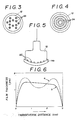
- the grooves (22) may comprise several holes (23) as shown in Fig. 3 or several concentric circular grooves (24) as shown in Fig. 4.
- the shape of an upper electrode (12) may be changed as shown in fig. 5. By this change, it is possible to increase the uniformity of the surface treatment.
- Fig. 7 shows an example of the reaction apparatus having a different structure from Fig. 2.
- the upper electrode (12) rotates and reagent gas is introduced into the reaction zone through gas nozzle (25).
- Fig. 10 shows an example in which the solid dielectric is provided only on the upper electrode.
- a heat resistant solid dielectric such as glass, ceramics, plastics or mica is provided on the surface of the upper electrode (12).
- the substrate (15) such as plate body is placed onto the upper surface of the lower electrode (13).
- the grooves (22) are for uniformly diffusing the glow discharge which is liable to concentrate at the edge and in the vicinity of the upper electrode (12), in Fig. 2, and cause glow discharge to diffuse over all parts of the surface of the upper electrode (12).
- a polyethylene film was obtained on the substrate surface at a film forming rate of 12,500 A/2 hr.
- the film was transparent, with satisfactory adhesion.
- a polyethylene film was formed in the same manner as in Example 1 under the following conditions:
- a polyethylene film was obtained at a film forming rate of 2,100 A/2 hr.
- the film was transparent, with satisfactory adhesion.
- a polyethylene film was formed in the same manner as in Example 1 under the following conditions:
- a polyethylene film was obtained at a film forming rate of 16,800 A/5.5 hr.
- the film was transparent, with a satisfactory adhesion.
- a polyethylene film was formed in the same manner as in Example 1 under the following conditions:
- a polyethylene film was obtained at a film forming rate of 9,000 A/2 hr.
- the film was transparent, with a satisfactory adhesion.
- a polyethylene film was thus formed on the surface of the aluminum substrate at a film forming rate of 11,417 A/2.
- the film was transparent, with excellent adhesion and a uniform film thickness.
- Example 6 The same treatment as in Example 6 was applied to a conductive graphite (already wrapped) as the substrate, under the conditions as shown in Table 2.
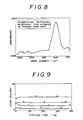
- a SiN x film was formed with the use of the apparatus shown in Fig. 7 under the following reaction conditions: He : 5,000 ml/min, H2 : 20 ml/min, N2 : 20 ml/min, SiCl4 : 4.5 mg/min, Pressure : Atmospheric pressure, RF : 13.56 MHz, 220 W, Temperature : 440°C Substrate : Si Wafer.
- Fig. 8 illustrates the difference in IR of the SiN x film thus obtained from the silicon substrate.
- Fig. 9 shows the result of XPS analysis in the depth direction of the SiN x film, which permits confirmation that nitrogen is contained in a large quantity.
- the film has the composition SiN x O y , and the content of oxygen thereof is controllable.
- a polyethylene film was formed from ethylene monomer under the following conditions: (a) Reaction gas flow rate: C2H4 : 3.0 SCCM, He : 4,500 SCCM, (b) Discharge: Atmospheric pressure, room temperature, 3,000 Hz, 1.0 kV, 1 to 5 mA (gradually increased), (c) Substrate: Silicon substrate
- a polyethylene film was formed on the silicon substrate at a film forming rate of 10,000 to 20,000 A/hr.
- the film was transparent, with satisfactory adhesion and a uniform film thickness.
- Example 12 a polyethylene terephthalate film was formed under the following conditions to make the surface thereof hydrophobic: (a) Reaction gas flow rate: CF4 : 25 SCCM, He : 210 SCCM, (b) Discharge: Atmospheric pressure, 3,000 Hz, 3.5 kV, 2 to 8 mA (gradually increased).
- the contact angle was measured five minutes after the start of treatment. The result showed a contact angle of 98°C. A non-treated film had a contact angle of 64°. The surface having become hydrophobic was thus confirmed. Treatment was uniform.
- Example 13 The same manner as in Example 13 was applied to a conductive graphite (already wrapped) as the substrate.
- the contact angle was measured 15 minutes after the start of treatment. The result showed a contact angle of 131°C. A non-treated film had a contact angle of 68°. The surface having become hydrophobic was confirmed. Treatment was uniform. In this Example, highly stable and uniformly dispersed glow discharge took place without the occurrence of arc discharge as in the Example 12, thus making available high-activity and high-stability plasma.
- the present invention is not limited to the above-mentioned examples. Variations are possible within the framework of the present invention in such details as the size and shape of the reaction vessel, the structure, configuration and shape of the electrodes, the shape and number of grooves on the lower surface of the upper electrode, and the structure and configuration of the reaction gas supply.
- the present invention as described above in detail, it is possible, as compared with the conventional low-pressure glow discharge plasma reaction, to eliminate the necessity of an apparatus and facilities for forming a vacuum system, reduce the cost, and carry out film formation and/or surface treatment under the atmospheric pressures, requiring only a relatively simple structure and configuration of the apparatus and facilitating treatment of a large-area substrate because the substrate can be set directly on the upper surface of the lower electrode.
- the present invention allows film formation and/or surface treatment without limiting the material, shape and properties of the substrate and makes available uniform film thickness and surface condition in a thin film so obtained.
Landscapes
- Chemical & Material Sciences (AREA)
- Engineering & Computer Science (AREA)
- Metallurgy (AREA)
- Chemical Kinetics & Catalysis (AREA)
- Materials Engineering (AREA)
- Mechanical Engineering (AREA)
- General Chemical & Material Sciences (AREA)
- Organic Chemistry (AREA)
- Inorganic Chemistry (AREA)
- Physics & Mathematics (AREA)
- Plasma & Fusion (AREA)
- Analytical Chemistry (AREA)
- Chemical Vapour Deposition (AREA)
- Plasma Technology (AREA)
Applications Claiming Priority (6)
| Application Number | Priority Date | Filing Date | Title |
|---|---|---|---|
| JP138630/88 | 1988-06-06 | ||
| JP13863088A JPH0248626B2 (ja) | 1988-06-06 | 1988-06-06 | Hakumakukeiseihohotosonosochi |
| JP63166599A JPH0672308B2 (ja) | 1988-07-04 | 1988-07-04 | 大気圧プラズマ反応方法 |
| JP166599/88 | 1988-07-04 | ||
| JP202977/88 | 1988-08-15 | ||
| JP63202977A JPH0748480B2 (ja) | 1988-08-15 | 1988-08-15 | 大気圧プラズマ反応方法 |
Publications (3)
| Publication Number | Publication Date |
|---|---|
| EP0346055A2 true EP0346055A2 (fr) | 1989-12-13 |
| EP0346055A3 EP0346055A3 (en) | 1990-02-07 |
| EP0346055B1 EP0346055B1 (fr) | 1995-04-19 |
Family
ID=27317713
Family Applications (1)
| Application Number | Title | Priority Date | Filing Date |
|---|---|---|---|
| EP89305671A Expired - Lifetime EP0346055B1 (fr) | 1988-06-06 | 1989-06-06 | Procédé pour provoquer une réaction dans le plasma sous pression atmosphérique |
Country Status (3)
| Country | Link |
|---|---|
| US (2) | US5126164A (fr) |
| EP (1) | EP0346055B1 (fr) |
| DE (1) | DE68922244T2 (fr) |
Cited By (19)
| Publication number | Priority date | Publication date | Assignee | Title |
|---|---|---|---|---|
| EP0327253A3 (en) * | 1988-02-01 | 1990-07-25 | Mitsui Toatsu Chemicals, Incorporated | Forming films, e.g. of amorphous silicon |
| EP0431951A3 (en) * | 1989-12-07 | 1991-11-06 | Research Development Corporation Of Japan | An atmospheric plasma reaction method and a device therefor |
| EP0508833A1 (fr) * | 1991-04-12 | 1992-10-14 | Bridgestone Corporation | Méthode et dispositif pour le traitement d'une surface |
| EP0533044A1 (fr) * | 1991-09-20 | 1993-03-24 | Balzers Aktiengesellschaft | Procédé et dispositif pour fabrication de revêtements protecteurs sur des substrats |
| US5286532A (en) * | 1991-08-20 | 1994-02-15 | Bridgestone Corporation | Method for producing golf balls |
| US5316739A (en) * | 1991-08-20 | 1994-05-31 | Bridgestone Corporation | Method and apparatus for surface treatment |
| AU666546B2 (en) * | 1992-06-17 | 1996-02-15 | L'air Liquide, Societe Anonyme Pour L'etude Et L'exploitation Des Procedes Georges Claude | Process for producing a silicon containing deposit at the surface of a metallic substrate, process for providing an anti-corrosive treatment, and metallized polymer support |
| DE19505449A1 (de) * | 1995-02-17 | 1996-08-22 | Fraunhofer Ges Forschung | Verfahren zur Herstellung eines Schichtsystems auf Substraten und das mit diesem Verfahren hergestellte Schichtsystem |
| FR2782837A1 (fr) * | 1998-08-28 | 2000-03-03 | Air Liquide | Procede et dispositif de traitement de surface par plasma a pression atmospherique |
| WO2001085635A1 (fr) * | 2000-05-10 | 2001-11-15 | Nkt Research A/S | Procede servant a revetir la surface d'un substrat inorganique par un materiau organique et produit obtenu |
| US6764658B2 (en) | 2002-01-08 | 2004-07-20 | Wisconsin Alumni Research Foundation | Plasma generator |
| EP1642598A3 (fr) * | 2002-04-02 | 2007-05-30 | Plasmasol Corporation | Systeme et procede pour injection d'un reactif organique dans un gaz faiblement ionise afin de generer des especes chimiquement actives |
| USRE41266E1 (en) | 1990-09-18 | 2010-04-27 | Lam Research Corporation | Composite electrode for plasma processes |
| EP2431195A3 (fr) * | 2010-09-20 | 2012-09-12 | The Goodyear Tire & Rubber Company | Pneu et procédé de fabrication d'un pneu ou composant de pneu |
| US8445074B2 (en) | 2010-04-01 | 2013-05-21 | The Goodyear Tire & Rubber Company | Atmospheric plasma treatment of tire cords |
| WO2013104949A3 (fr) * | 2012-01-09 | 2014-03-20 | L'université De Genève | Procédé de traitement d'un objet |
| US9133360B2 (en) | 2010-04-01 | 2015-09-15 | The Goodyear Tire & Rubber Company | Atmospheric plasma treatment of reinforcement cords and use in rubber articles |
| US9433971B2 (en) | 2012-10-04 | 2016-09-06 | The Goodyear Tire & Rubber Company | Atmospheric plasma treatment of reinforcement cords and use in rubber articles |
| US9441325B2 (en) | 2012-10-04 | 2016-09-13 | The Goodyear Tire & Rubber Company | Atmospheric plasma treatment of reinforcement cords and use in rubber articles |
Families Citing this family (53)
| Publication number | Priority date | Publication date | Assignee | Title |
|---|---|---|---|---|
| JP2929651B2 (ja) * | 1990-03-14 | 1999-08-03 | 株式会社ブリヂストン | ゴム系複合材料の製造方法 |
| JP2897055B2 (ja) * | 1990-03-14 | 1999-05-31 | 株式会社ブリヂストン | ゴム系複合材料の製造方法 |
| US5262097A (en) * | 1990-07-03 | 1993-11-16 | Allergan, Inc. | Methods for attaching fixation members to optics of intraocular lenses |
| US5578130A (en) * | 1990-12-12 | 1996-11-26 | Semiconductor Energy Laboratory Co., Ltd. | Apparatus and method for depositing a film |
| JP2840699B2 (ja) * | 1990-12-12 | 1998-12-24 | 株式会社 半導体エネルギー研究所 | 被膜形成装置及び被膜形成方法 |
| US5628883A (en) * | 1991-06-18 | 1997-05-13 | Japan Vilene Co. Ltd. | Method for generating and activating plasma process of treatment using same, and apparatus therefor |
| US5399832A (en) * | 1991-08-05 | 1995-03-21 | Kimoto Co., Ltd. | Process and apparatus for using atmospheric-pressure plasma reactions |
| US7264850B1 (en) | 1992-12-28 | 2007-09-04 | Semiconductor Energy Laboratory Co., Ltd. | Process for treating a substrate with a plasma |
| WO1994022628A1 (fr) * | 1993-04-05 | 1994-10-13 | Seiko Epson Corporation | Procede et appareil d'assemblage par brasage |
| US6835523B1 (en) * | 1993-05-09 | 2004-12-28 | Semiconductor Energy Laboratory Co., Ltd. | Apparatus for fabricating coating and method of fabricating the coating |
| US5423929A (en) * | 1993-10-27 | 1995-06-13 | Allergan, Inc. | Intraocular lenses and methods for producing same |
| JP3312377B2 (ja) * | 1993-12-09 | 2002-08-05 | セイコーエプソン株式会社 | ろう材による接合方法及び装置 |
| US6342275B1 (en) * | 1993-12-24 | 2002-01-29 | Seiko Epson Corporation | Method and apparatus for atmospheric pressure plasma surface treatment, method of manufacturing semiconductor device, and method of manufacturing ink jet printing head |
| US6006763A (en) * | 1995-01-11 | 1999-12-28 | Seiko Epson Corporation | Surface treatment method |
| JP3521587B2 (ja) * | 1995-02-07 | 2004-04-19 | セイコーエプソン株式会社 | 基板周縁の不要物除去方法及び装置並びにそれを用いた塗布方法 |
| JPH08279495A (ja) * | 1995-02-07 | 1996-10-22 | Seiko Epson Corp | プラズマ処理装置及びその方法 |
| US6255718B1 (en) | 1995-02-28 | 2001-07-03 | Chip Express Corporation | Laser ablateable material |
| WO1996031997A1 (fr) * | 1995-04-07 | 1996-10-10 | Seiko Epson Corporation | Equipement de traitement de surface |
| JP3598602B2 (ja) * | 1995-08-07 | 2004-12-08 | セイコーエプソン株式会社 | プラズマエッチング方法、液晶表示パネルの製造方法、及びプラズマエッチング装置 |
| JPH09233862A (ja) * | 1995-12-18 | 1997-09-05 | Seiko Epson Corp | 圧電体を用いた発電方法、発電装置および電子機器 |
| US5776553A (en) * | 1996-02-23 | 1998-07-07 | Saint Gobain/Norton Industrial Ceramics Corp. | Method for depositing diamond films by dielectric barrier discharge |
| JPH09312545A (ja) | 1996-03-18 | 1997-12-02 | Seiko Epson Corp | 圧電素子、その製造方法、及び圧電振動片のマウント装置 |
| US5918354A (en) * | 1996-04-02 | 1999-07-06 | Seiko Epson Corporation | Method of making a piezoelectric element |
| US6082294A (en) * | 1996-06-07 | 2000-07-04 | Saint-Gobain Industrial Ceramics, Inc. | Method and apparatus for depositing diamond film |
| US5902523A (en) * | 1996-06-26 | 1999-05-11 | Allergan | IOLs and production methods for same |
| US5972176A (en) * | 1997-10-03 | 1999-10-26 | 3M Innovative Properties Company | Corona treatment of polymers |
| US20030066746A1 (en) * | 1997-12-04 | 2003-04-10 | Korea Institute Of Science And Technology | Plasma polymerization enhancement of surface of metal for use in refrigerating and air conditioning |
| WO2000070117A1 (fr) * | 1999-05-14 | 2000-11-23 | The Regents Of The University Of California | Dispositif de flux de plasma a grande plage de pressions compatible a basse temperature |
| US7091605B2 (en) | 2001-09-21 | 2006-08-15 | Eastman Kodak Company | Highly moisture-sensitive electronic device element and method for fabrication |
| US20030042129A1 (en) * | 2000-04-06 | 2003-03-06 | Korea Institute Of Science And Technology | Plasma polymerization enhancement of surface of metal for use in refrigerating and air conditioning |
| KR100386526B1 (ko) * | 2000-10-02 | 2003-06-02 | 우형철 | 다공성 전극을 이용하는 상압 플라즈마 장치 |
| US20020124962A1 (en) * | 2001-03-12 | 2002-09-12 | Selwyn Gary S. | Atmospheric pressure plasma etching reactor |
| WO2003019624A2 (fr) * | 2001-08-27 | 2003-03-06 | University Of New Hampshire | Procede de decharge a barriere dielectrique pour le depot de film au nitrure de silicium sur des substrats |
| US6869645B2 (en) * | 2001-10-23 | 2005-03-22 | Acushnet Company | Method for plasma treatment of golf balls |
| US6923886B2 (en) * | 2001-10-23 | 2005-08-02 | Acushnet Company | Apparatus for plasma treatment of golf balls |
| US20030168009A1 (en) * | 2002-03-08 | 2003-09-11 | Denes Ferencz S. | Plasma processing within low-dimension cavities |
| KR20030081742A (ko) * | 2002-04-12 | 2003-10-22 | 우형철 | 플라즈마를 이용한 에칭처리장치 |
| US6936546B2 (en) * | 2002-04-26 | 2005-08-30 | Accretech Usa, Inc. | Apparatus for shaping thin films in the near-edge regions of in-process semiconductor substrates |
| US7288204B2 (en) * | 2002-07-19 | 2007-10-30 | Fuji Photo Film B.V. | Method and arrangement for treating a substrate with an atmospheric pressure glow plasma (APG) |
| US7220687B2 (en) * | 2004-06-25 | 2007-05-22 | Applied Materials, Inc. | Method to improve water-barrier performance by changing film surface morphology |
| WO2006007313A2 (fr) * | 2004-06-25 | 2006-01-19 | Applied Materials, Inc. | Pouvoir d'etancheite a l'eau ameliore pour film d'enrobage |
| US7214600B2 (en) * | 2004-06-25 | 2007-05-08 | Applied Materials, Inc. | Method to improve transmittance of an encapsulating film |
| US20060040067A1 (en) * | 2004-08-23 | 2006-02-23 | Thomas Culp | Discharge-enhanced atmospheric pressure chemical vapor deposition |
| WO2007007995A1 (fr) * | 2005-07-09 | 2007-01-18 | Bang-Kwon Kang | Procédé de revêtement d’une surface pour un traitement hydrophobe et superhydrophobe dans un plasma à pression atmosphérique |
| US20080044588A1 (en) * | 2006-08-15 | 2008-02-21 | Sakhrani Vinay G | Method for Treating a Hydrophilic Surface |
| US8084103B2 (en) * | 2006-08-15 | 2011-12-27 | Sakhrani Vinay G | Method for treating a hydrophilic surface |
| US20080113103A1 (en) * | 2006-11-10 | 2008-05-15 | Ppg Industries Ohio, Inc. | Halogen treatment of polymer films using atmospheric plasma |
| FR2911610B1 (fr) * | 2007-01-24 | 2012-09-21 | Air Liquide | Procede de traitement de surface de substrats polymeres, substrats ainsi obtenus et leur utilisation pour la realisation de materiaux multicouches. |
| US20080241355A1 (en) * | 2007-03-30 | 2008-10-02 | Applied Materials, Inc. | Thin film transistor devices having high electron mobility and stability |
| TWI386640B (zh) * | 2008-09-26 | 2013-02-21 | Advanced Semiconductor Eng | 基材表面疏水性處理之偵測方法 |
| WO2011007653A1 (fr) * | 2009-07-13 | 2011-01-20 | 日本碍子株式会社 | Procédé de fabrication d'un corps de film de carbone de type diamant |
| US9133412B2 (en) | 2012-07-09 | 2015-09-15 | Tribofilm Research, Inc. | Activated gaseous species for improved lubrication |
| KR102156795B1 (ko) * | 2013-05-15 | 2020-09-17 | 에이에스엠 아이피 홀딩 비.브이. | 증착 장치 |
Family Cites Families (20)
| Publication number | Priority date | Publication date | Assignee | Title |
|---|---|---|---|---|
| US4292384A (en) * | 1977-09-30 | 1981-09-29 | Horizons Research Incorporated | Gaseous plasma developing and etching process employing low voltage DC generation |
| FR2411897A2 (fr) * | 1977-12-13 | 1979-07-13 | Alsthom Atlantique | Procede de depot d'une couche mince par decomposition d'un gaz dans un plasma |
| US4223048A (en) * | 1978-08-07 | 1980-09-16 | Pacific Western Systems | Plasma enhanced chemical vapor processing of semiconductive wafers |
| JPS5642377A (en) * | 1979-09-14 | 1981-04-20 | Fujitsu Ltd | Ultraviolet ray erasable type rewritable read-only memory |
| JPS58175824A (ja) * | 1983-03-28 | 1983-10-15 | Semiconductor Energy Lab Co Ltd | プラズマ気相反応用装置 |
| JPS59211219A (ja) * | 1983-05-16 | 1984-11-30 | Mitsubishi Electric Corp | プラズマcvd装置 |
| JPS6013065A (ja) * | 1983-07-01 | 1985-01-23 | Stanley Electric Co Ltd | 固体表面の撥水性処理方法 |
| JPS60258914A (ja) * | 1984-06-05 | 1985-12-20 | Ricoh Co Ltd | プラズマcvd装置 |
| JPS6134031A (ja) * | 1984-07-26 | 1986-02-18 | Nippon Paint Co Ltd | 表面処理装置 |
| US4616597A (en) * | 1984-10-31 | 1986-10-14 | Rca Corporation | Apparatus for making a plasma coating |
| JPS61238961A (ja) * | 1985-04-12 | 1986-10-24 | Sachiko Okazaki | 基材表面の改質方法 |
| JPS6269620A (ja) * | 1985-09-24 | 1987-03-30 | Anelva Corp | プラズマ処理装置 |
| JPS62163743A (ja) * | 1986-01-11 | 1987-07-20 | Nippon Paint Co Ltd | 表面処理法 |
| DE3606959A1 (de) * | 1986-03-04 | 1987-09-10 | Leybold Heraeus Gmbh & Co Kg | Vorrichtung zur plasmabehandlung von substraten in einer durch hochfrequenz angeregten plasmaentladung |
| JPS63117906A (ja) * | 1986-11-07 | 1988-05-21 | Shin Etsu Chem Co Ltd | 多結晶シリコン製造装置用部材 |
| JPS63310795A (ja) * | 1987-06-11 | 1988-12-19 | Fujitsu Ltd | マイクロ波プラズマジェットによるダイヤモンド気相合成方法 |
| US4834020A (en) * | 1987-12-04 | 1989-05-30 | Watkins-Johnson Company | Atmospheric pressure chemical vapor deposition apparatus |
| US5031571A (en) * | 1988-02-01 | 1991-07-16 | Mitsui Toatsu Chemicals, Inc. | Apparatus for forming a thin film on a substrate |
| JP2990608B2 (ja) * | 1989-12-13 | 1999-12-13 | 株式会社ブリヂストン | 表面処理方法 |
| JP3063769B2 (ja) * | 1990-07-17 | 2000-07-12 | イーシー化学株式会社 | 大気圧プラズマ表面処理法 |
-
1989
- 1989-06-06 EP EP89305671A patent/EP0346055B1/fr not_active Expired - Lifetime
- 1989-06-06 DE DE68922244T patent/DE68922244T2/de not_active Expired - Lifetime
-
1990
- 1990-05-14 US US07/522,462 patent/US5126164A/en not_active Expired - Lifetime
-
1995
- 1995-03-09 US US08/401,290 patent/US5733610A/en not_active Expired - Lifetime
Cited By (24)
| Publication number | Priority date | Publication date | Assignee | Title |
|---|---|---|---|---|
| EP0327253A3 (en) * | 1988-02-01 | 1990-07-25 | Mitsui Toatsu Chemicals, Incorporated | Forming films, e.g. of amorphous silicon |
| EP0431951A3 (en) * | 1989-12-07 | 1991-11-06 | Research Development Corporation Of Japan | An atmospheric plasma reaction method and a device therefor |
| USRE41266E1 (en) | 1990-09-18 | 2010-04-27 | Lam Research Corporation | Composite electrode for plasma processes |
| EP0508833A1 (fr) * | 1991-04-12 | 1992-10-14 | Bridgestone Corporation | Méthode et dispositif pour le traitement d'une surface |
| US5225659A (en) * | 1991-04-12 | 1993-07-06 | Bridgestone Corporation | Method and apparatus for surface treating an axially symmetric substrate at atmosphere pressure |
| US5286532A (en) * | 1991-08-20 | 1994-02-15 | Bridgestone Corporation | Method for producing golf balls |
| US5316739A (en) * | 1991-08-20 | 1994-05-31 | Bridgestone Corporation | Method and apparatus for surface treatment |
| EP0533044A1 (fr) * | 1991-09-20 | 1993-03-24 | Balzers Aktiengesellschaft | Procédé et dispositif pour fabrication de revêtements protecteurs sur des substrats |
| US5298290A (en) * | 1991-09-20 | 1994-03-29 | Balzers Aktiengesellschaft | Protective coating on substrates |
| AU666546B2 (en) * | 1992-06-17 | 1996-02-15 | L'air Liquide, Societe Anonyme Pour L'etude Et L'exploitation Des Procedes Georges Claude | Process for producing a silicon containing deposit at the surface of a metallic substrate, process for providing an anti-corrosive treatment, and metallized polymer support |
| DE19505449A1 (de) * | 1995-02-17 | 1996-08-22 | Fraunhofer Ges Forschung | Verfahren zur Herstellung eines Schichtsystems auf Substraten und das mit diesem Verfahren hergestellte Schichtsystem |
| US6299948B1 (en) | 1998-08-28 | 2001-10-09 | L'air Liquide, Societe Anonyme Pour L'etude Et L'exploitation Des Procedes Georges Claude | Method and device for surface treatment with a plasma at atmospheric pressure |
| WO2000013202A1 (fr) * | 1998-08-28 | 2000-03-09 | L'air Liquide, Societe Anonyme Pour L'etude Et L'exploitation Des Procedes Georges Claude | Procede et dispositif de traitement de surface par plasma a pression atmospherique |
| FR2782837A1 (fr) * | 1998-08-28 | 2000-03-03 | Air Liquide | Procede et dispositif de traitement de surface par plasma a pression atmospherique |
| WO2001085635A1 (fr) * | 2000-05-10 | 2001-11-15 | Nkt Research A/S | Procede servant a revetir la surface d'un substrat inorganique par un materiau organique et produit obtenu |
| US7238395B2 (en) | 2000-05-10 | 2007-07-03 | Nkt Research A/S | Method of coating the surface of an inorganic substrates with an organic material and the product obtained |
| US6764658B2 (en) | 2002-01-08 | 2004-07-20 | Wisconsin Alumni Research Foundation | Plasma generator |
| EP1642598A3 (fr) * | 2002-04-02 | 2007-05-30 | Plasmasol Corporation | Systeme et procede pour injection d'un reactif organique dans un gaz faiblement ionise afin de generer des especes chimiquement actives |
| US8445074B2 (en) | 2010-04-01 | 2013-05-21 | The Goodyear Tire & Rubber Company | Atmospheric plasma treatment of tire cords |
| US9133360B2 (en) | 2010-04-01 | 2015-09-15 | The Goodyear Tire & Rubber Company | Atmospheric plasma treatment of reinforcement cords and use in rubber articles |
| EP2431195A3 (fr) * | 2010-09-20 | 2012-09-12 | The Goodyear Tire & Rubber Company | Pneu et procédé de fabrication d'un pneu ou composant de pneu |
| WO2013104949A3 (fr) * | 2012-01-09 | 2014-03-20 | L'université De Genève | Procédé de traitement d'un objet |
| US9433971B2 (en) | 2012-10-04 | 2016-09-06 | The Goodyear Tire & Rubber Company | Atmospheric plasma treatment of reinforcement cords and use in rubber articles |
| US9441325B2 (en) | 2012-10-04 | 2016-09-13 | The Goodyear Tire & Rubber Company | Atmospheric plasma treatment of reinforcement cords and use in rubber articles |
Also Published As
| Publication number | Publication date |
|---|---|
| DE68922244D1 (de) | 1995-05-24 |
| EP0346055A3 (en) | 1990-02-07 |
| US5733610A (en) | 1998-03-31 |
| DE68922244T2 (de) | 1995-09-14 |
| US5126164A (en) | 1992-06-30 |
| EP0346055B1 (fr) | 1995-04-19 |
Similar Documents
| Publication | Publication Date | Title |
|---|---|---|
| EP0346055B1 (fr) | Procédé pour provoquer une réaction dans le plasma sous pression atmosphérique | |
| EP0303508B1 (fr) | Distributeur d'admission et procédés pour l'augmentation de la dissociation de gaz et pour le PECVD de films diélectriques | |
| US5185132A (en) | Atomspheric plasma reaction method and apparatus therefor | |
| US5271972A (en) | Method for depositing ozone/TEOS silicon oxide films of reduced surface sensitivity | |
| US5356722A (en) | Method for depositing ozone/TEOS silicon oxide films of reduced surface sensitivity | |
| EP1148150B1 (fr) | Procédé et appareillage pour le traitement des substrats de sémiconducteur par des radicaux hydroxylés | |
| KR100687530B1 (ko) | 플라즈마 cvd 막 형성장치 | |
| US4491496A (en) | Enclosure for the treatment, and particularly for the etching of substrates by the reactive plasma method | |
| EP0090586A1 (fr) | Procédé de traitement par plasma avec circulation de gaz | |
| US4718976A (en) | Process and apparatus for plasma treatment | |
| US6514880B2 (en) | Siloxan polymer film on semiconductor substrate and method for forming same | |
| US6649545B2 (en) | Photo-assisted remote plasma apparatus and method | |
| Schmidt-Szalowski et al. | Thin films deposition from hexamethyldisiloxane and hexamethyldisilazane under dielectric-barrier discharge (DBD) conditions | |
| JPH04358076A (ja) | 大気圧プラズマ反応方法とその装置 | |
| JPH083749A (ja) | プラズマ励起cvdによるシリコンオキシナイトライド膜の堆積方法 | |
| US4936940A (en) | Equipment for surface treatment | |
| US20020192982A1 (en) | Method of forming a carbon doped oxide layer on a substrate | |
| US5275665A (en) | Method and apparatus for causing plasma reaction under atmospheric pressure | |
| JPH0215171A (ja) | 大気圧プラズマ反応方法 | |
| US5061514A (en) | Chemical vapor deposition (CVD) process for plasma depositing silicon carbide films onto a substrate | |
| JPH06168937A (ja) | シリコン酸化膜の製造方法 | |
| JPH03241739A (ja) | 大気圧プラズマ反応方法 | |
| US7763551B2 (en) | RLSA CVD deposition control using halogen gas for hydrogen scavenging | |
| US6759344B2 (en) | Method for forming low dielectric constant interlayer insulation film | |
| JPH03229886A (ja) | 大気圧グロープラズマエッチング方法 |
Legal Events
| Date | Code | Title | Description |
|---|---|---|---|
| PUAI | Public reference made under article 153(3) epc to a published international application that has entered the european phase |
Free format text: ORIGINAL CODE: 0009012 |
|
| AK | Designated contracting states |
Kind code of ref document: A2 Designated state(s): CH DE FR IT LI NL |
|
| PUAL | Search report despatched |
Free format text: ORIGINAL CODE: 0009013 |
|
| AK | Designated contracting states |
Kind code of ref document: A3 Designated state(s): CH DE FR IT LI NL |
|
| 17P | Request for examination filed |
Effective date: 19900414 |
|
| 17Q | First examination report despatched |
Effective date: 19911008 |
|
| GRAA | (expected) grant |
Free format text: ORIGINAL CODE: 0009210 |
|
| AK | Designated contracting states |
Kind code of ref document: B1 Designated state(s): CH DE FR IT LI NL |
|
| REF | Corresponds to: |
Ref document number: 68922244 Country of ref document: DE Date of ref document: 19950524 |
|
| ITF | It: translation for a ep patent filed | ||
| ET | Fr: translation filed | ||
| PLBE | No opposition filed within time limit |
Free format text: ORIGINAL CODE: 0009261 |
|
| STAA | Information on the status of an ep patent application or granted ep patent |
Free format text: STATUS: NO OPPOSITION FILED WITHIN TIME LIMIT |
|
| 26N | No opposition filed | ||
| REG | Reference to a national code |
Ref country code: CH Ref legal event code: PFA Owner name: RESEARCH DEVELOPMENT CORPORATION OF JAPAN Free format text: RESEARCH DEVELOPMENT CORPORATION OF JAPAN#5-2, 2-CHOME, NAGATO-CHO#CHIYODA-KU/TOKYO (JP) -TRANSFER TO- RESEARCH DEVELOPMENT CORPORATION OF JAPAN#5-2, 2-CHOME, NAGATO-CHO#CHIYODA-KU/TOKYO (JP) |
|
| PGFP | Annual fee paid to national office [announced via postgrant information from national office to epo] |
Ref country code: CH Payment date: 20080613 Year of fee payment: 20 |
|
| PGFP | Annual fee paid to national office [announced via postgrant information from national office to epo] |
Ref country code: IT Payment date: 20080625 Year of fee payment: 20 |
|
| PGFP | Annual fee paid to national office [announced via postgrant information from national office to epo] |
Ref country code: NL Payment date: 20080618 Year of fee payment: 20 Ref country code: DE Payment date: 20080620 Year of fee payment: 20 |
|
| PGFP | Annual fee paid to national office [announced via postgrant information from national office to epo] |
Ref country code: FR Payment date: 20080613 Year of fee payment: 20 |
|
| REG | Reference to a national code |
Ref country code: CH Ref legal event code: PL |
|
| PG25 | Lapsed in a contracting state [announced via postgrant information from national office to epo] |
Ref country code: NL Free format text: LAPSE BECAUSE OF EXPIRATION OF PROTECTION Effective date: 20090606 |
|
| NLV7 | Nl: ceased due to reaching the maximum lifetime of a patent |
Effective date: 20090606 |