EP0346571A2 - Festkörper-Relais - Google Patents
Festkörper-Relais Download PDFInfo
- Publication number
- EP0346571A2 EP0346571A2 EP89104238A EP89104238A EP0346571A2 EP 0346571 A2 EP0346571 A2 EP 0346571A2 EP 89104238 A EP89104238 A EP 89104238A EP 89104238 A EP89104238 A EP 89104238A EP 0346571 A2 EP0346571 A2 EP 0346571A2
- Authority
- EP
- European Patent Office
- Prior art keywords
- solid state
- output device
- state relay
- emitting diode
- light emitting
- Prior art date
- Legal status (The legal status is an assumption and is not a legal conclusion. Google has not performed a legal analysis and makes no representation as to the accuracy of the status listed.)
- Withdrawn
Links
- 239000007787 solid Substances 0.000 title claims abstract description 30
- 229910021420 polycrystalline silicon Inorganic materials 0.000 claims description 9
- 229920005591 polysilicon Polymers 0.000 claims description 9
- XUIMIQQOPSSXEZ-UHFFFAOYSA-N Silicon Chemical compound [Si] XUIMIQQOPSSXEZ-UHFFFAOYSA-N 0.000 claims description 4
- 230000008878 coupling Effects 0.000 claims description 4
- 238000010168 coupling process Methods 0.000 claims description 4
- 238000005859 coupling reaction Methods 0.000 claims description 4
- 230000007935 neutral effect Effects 0.000 claims description 4
- 229910052710 silicon Inorganic materials 0.000 claims description 4
- 239000010703 silicon Substances 0.000 claims description 4
- 230000005669 field effect Effects 0.000 claims description 2
- 238000007599 discharging Methods 0.000 claims 3
- 230000001052 transient effect Effects 0.000 abstract description 15
- 230000036039 immunity Effects 0.000 abstract description 3
- 238000010586 diagram Methods 0.000 description 7
- 238000002955 isolation Methods 0.000 description 7
- 230000003287 optical effect Effects 0.000 description 5
- 235000014676 Phragmites communis Nutrition 0.000 description 3
- 238000000034 method Methods 0.000 description 3
- 230000004913 activation Effects 0.000 description 2
- 239000003990 capacitor Substances 0.000 description 2
- 230000008859 change Effects 0.000 description 2
- 239000004020 conductor Substances 0.000 description 2
- 230000008021 deposition Effects 0.000 description 2
- 229910052751 metal Inorganic materials 0.000 description 2
- 239000002184 metal Substances 0.000 description 2
- 150000004767 nitrides Chemical class 0.000 description 2
- 230000002146 bilateral effect Effects 0.000 description 1
- 230000015572 biosynthetic process Effects 0.000 description 1
- 230000015556 catabolic process Effects 0.000 description 1
- 230000005684 electric field Effects 0.000 description 1
- 238000005516 engineering process Methods 0.000 description 1
- 238000005286 illumination Methods 0.000 description 1
- 230000006872 improvement Effects 0.000 description 1
- AMGQUBHHOARCQH-UHFFFAOYSA-N indium;oxotin Chemical compound [In].[Sn]=O AMGQUBHHOARCQH-UHFFFAOYSA-N 0.000 description 1
- 238000004519 manufacturing process Methods 0.000 description 1
- 230000003071 parasitic effect Effects 0.000 description 1
- 238000002161 passivation Methods 0.000 description 1
- 230000004044 response Effects 0.000 description 1
- 239000000758 substrate Substances 0.000 description 1
Images

Classifications
-
- H—ELECTRICITY
- H01—ELECTRIC ELEMENTS
- H01H—ELECTRIC SWITCHES; RELAYS; SELECTORS; EMERGENCY PROTECTIVE DEVICES
- H01H51/00—Electromagnetic relays
-
- H—ELECTRICITY
- H03—ELECTRONIC CIRCUITRY
- H03K—PULSE TECHNIQUE
- H03K17/00—Electronic switching or gating, i.e. not by contact-making and –breaking
- H03K17/51—Electronic switching or gating, i.e. not by contact-making and –breaking characterised by the components used
- H03K17/56—Electronic switching or gating, i.e. not by contact-making and –breaking characterised by the components used by the use, as active elements, of semiconductor devices
- H03K17/687—Electronic switching or gating, i.e. not by contact-making and –breaking characterised by the components used by the use, as active elements, of semiconductor devices the devices being field-effect transistors
- H03K17/6871—Electronic switching or gating, i.e. not by contact-making and –breaking characterised by the components used by the use, as active elements, of semiconductor devices the devices being field-effect transistors the output circuit comprising more than one controlled field-effect transistor
- H03K17/6874—Electronic switching or gating, i.e. not by contact-making and –breaking characterised by the components used by the use, as active elements, of semiconductor devices the devices being field-effect transistors the output circuit comprising more than one controlled field-effect transistor in a symmetrical configuration
-
- H—ELECTRICITY
- H03—ELECTRONIC CIRCUITRY
- H03K—PULSE TECHNIQUE
- H03K17/00—Electronic switching or gating, i.e. not by contact-making and –breaking
- H03K17/04—Modifications for accelerating switching
- H03K17/042—Modifications for accelerating switching by feedback from the output circuit to the control circuit
- H03K17/04206—Modifications for accelerating switching by feedback from the output circuit to the control circuit in field-effect transistor switches
-
- H—ELECTRICITY
- H03—ELECTRONIC CIRCUITRY
- H03K—PULSE TECHNIQUE
- H03K17/00—Electronic switching or gating, i.e. not by contact-making and –breaking
- H03K17/16—Modifications for eliminating interference voltages or currents
- H03K17/161—Modifications for eliminating interference voltages or currents in field-effect transistor switches
- H03K17/162—Modifications for eliminating interference voltages or currents in field-effect transistor switches without feedback from the output circuit to the control circuit
-
- H—ELECTRICITY
- H03—ELECTRONIC CIRCUITRY
- H03K—PULSE TECHNIQUE
- H03K17/00—Electronic switching or gating, i.e. not by contact-making and –breaking
- H03K17/16—Modifications for eliminating interference voltages or currents
- H03K17/161—Modifications for eliminating interference voltages or currents in field-effect transistor switches
- H03K17/165—Modifications for eliminating interference voltages or currents in field-effect transistor switches by feedback from the output circuit to the control circuit
-
- H—ELECTRICITY
- H03—ELECTRONIC CIRCUITRY
- H03K—PULSE TECHNIQUE
- H03K17/00—Electronic switching or gating, i.e. not by contact-making and –breaking
- H03K17/51—Electronic switching or gating, i.e. not by contact-making and –breaking characterised by the components used
- H03K17/78—Electronic switching or gating, i.e. not by contact-making and –breaking characterised by the components used using opto-electronic devices, i.e. light-emitting and photoelectric devices electrically- or optically-coupled
- H03K17/785—Electronic switching or gating, i.e. not by contact-making and –breaking characterised by the components used using opto-electronic devices, i.e. light-emitting and photoelectric devices electrically- or optically-coupled controlling field-effect transistor switches
Definitions
- a solid state relay provides isolation between a control circuit and a switched circuit and may replace an electromechanical device such as a reed relay.
- a typical solid state relay consists of a light emitting diode (LED) optically coupled across an electrically isolating gap to a photodiode array.
- the photodiode array is electrically connected to a output device such as a field effect transistor (FET).
- FET field effect transistor
- the relay disclosed in U.S. Patent 4,390,790 to Rodriguez includes a photodiode array directly connected to an output FET.
- Rodriguez's use of a turn-off transistor to discharge the output FET gate to source capacitance provides some improvement in turn-off speed but provides no transient protection to the relay.
- Relays such as this are vulnerable not only to transient propagation between the control and switched circuits but also to transient induced false turn-on and turn-off.
- a solid state relay has improved turn-off characteristics and a high degree of transient immunity.
- the relay includes an optically controlled active series and shunt enhancement circuit located between the photodiode array and a pair of output FETs.
- Series phototransistors in the enhancement circuit actively couple and decouple the array from the output FETs at turn-on and turn-off.
- a shunt FET and a shunt silicon controlled rectifier (SCR) create rapid discharge paths for the output FET gate to source capacitances at turn-off.
- a shunt transistor is capacitively coupled to the relay output to protect against transient induced false turn-ons.
- the solid state relay includes a shield over the photodiode array.
- Use of the shield allows direct and close optical coupling between the LED and the photodiode array so that high speed can be achieved at low required LED currents.
- the shield is both optically transmissive and electrically conductive and is connected to ground or to another neutral part of the relay circuit. The shield is positioned to intercept control circuit transients so that false turn-on caused by electrical activation of the photodiode array or other components can be avoided.
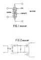
- Figure 1 shows a well known reed relay that may be used to provide isolation between a control circuit and a switched circuit.
- Electromechanical devices such as reed relays have inherent disadvantages due to the use of mechanical moving parts.
- FIG 2 is a schematic diagram of a prior art solid state relay disclosed by Rodriguez in U.S. Patent 4,390,790. Activation of the LED by the control circuit creates a voltage across the photodiode array which turns on the output FETs.
- the shunt resistor accelerates the discharge of the FET capacitances at turn-off but slows turn-on of the relay.
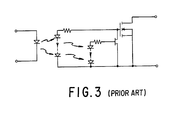
- Figure 3 is a schematic diagram of another prior art solid state relay disclosed by the Rodriguez patent. The shunt resistor is replaced by a shunt FET which is activated by a second photodiode array.
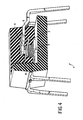
- FIG. 4 is a cut-away view of a packaged solid state relay 1 constructed in accordance with a preferred embodiment of the present invention.
- the relay 1 may be constructed using known lead frame technology of the type disclosed in U.S. Patent 4,694,183 issued on September 15, 1987 to Merrick, et. al.
- An LED 3 is separated from an integrated circuit (IC) 5 containing the remainder of the relay circuitry by a gap 9 including an optically transmissive light guide 11 and an insulating film 7.
- Total relay 1 input to output resistance is approximately 50 gigaohms.
- LED 3 could be located in the same plane as IC 5 and gap 9 would then be a curved path rather than the straight path shown in Figure 4 for face-to-face positioning.
- FIG. 5 is a schematic diagram of the relay 1 shown in Figure 4.
- the entire circuit, except for LED 3, is fabricated as one IC 5 on a single silicon chip.
- Known dielectric isolation techniques described in U.S. Patent 4,390,790 are used to provide necessary electrical isolation between various components of the circuit.
- a photodiode array I3 has ten individual photodiodes and generates an on-voltage of approximately 5 volts in response to a 5 mA current through LED 3. This on-voltage is coupled, through phototransistors 33 and 35, across the gates-to-sources of output FETs 15 and 17.
- These output FETs 15, 17 are vertical double diffused MOS (DMOS) devices constructed in dielectric isolation tubs.
- DMOS vertical double diffused MOS
- the sources of the two FETs 15, 17 are connected together to achieve the desired high, 230 volt, bilateral breakdown voltage despite the existence of parasitic diodes between the sources and drains.
- Output on-resistance is approximately 200 ohms.
- Output terminals 19, 21 provide a low impedance path when the relay 1 is on and allow connection to the circuit to be switched.
- Source terminal 23 may be a ground or neutral connection of the switched circuit. The voltage at terminal 23 will remain one diode drop voltage (about 0.7 volts) above the lower of the voltages at terminal 19 or 21. Alternatively, in D.C. switching (between terminal 23 and either of terminals 19 or 21) terminal 23 will remain at the most negative voltage of any of the three terminals.
- Figure 6 is a block diagram representation of an enhancement circuit 31 located between the array 13 and the output FETs 15, 17 shown in Figure 5.
- the enhancement circuit 31 provides enhanced turn-on less (less than 250 microseconds), turn-off (less than 100 microseconds) and transient immunity characteristics to the relay 1.
- circuit 31 may be modelled as a series and shunt combination of optically controlled active switches including series switches 41, 43 and shunt switches 45, 47 and 49.
- Switches 41 and 43 are two series phototransistors 33, 35 which couple and decouple the gates and sources of the output FETs 15, 17 from the photodiode array 13.
- Switch 45 is a silicon controlled rectifier 51 made up of transistors 53, 55. SCR 51 is connected from gates to sources of the output FETs 15, 17 and is controlled by the phototransistors 33, 35 and a FET 61.
- the base-emitter junction of pnp transistor 57 is connected across phototransistor 33 and the collector is connected to the gate of FET 61.
- Switch 47 is a transistor 63 connected across the gate to source path of the output FETs 15, 17.
- the base of transistor 63 is capacitively coupled through capacitors 65, 67 to the output terminals 19, 21, and is also connected to the drain of a FET 69.
- Photodiodes 71, 73 are activated by light from LED 3 and are connected from the gate to the source of FET 69.
- Switch 49 is a FET 75 shunting the gate to source of the output FETs 15, 17 and controlled by photodiodes 71, 73.
- a current is passed through LED 3 causing it to emit light.
- This light is coupled across gap 9 to array 13 which presents a nominal 5 volts at the input to enhancement circuit 31.
- the light also activates phototransistors 33, 35 which couple the array 13 voltage to output FETs 15, 17.
- This voltage significantly exceeds the 1.1 volt threshhold of the FETs 15, 17 and ensures turn-on.
- the light from LED 3 illuminates photodiodes 71, 73 and causes them to generate a voltage of approximately 1 volt.
- This voltage turns off FET 75 (shunt switch 49) and FET 61 amd turns on FET 69 which shunts the base-emitter junction of transistor 63 (switch 47) and turns it off.
- transistor 63 When this occurs, the drain of one of the output FETs begins to move towards a positive voltage and this voltage change, through capacitor 65 or 67, causes transistor 63 to turn on. Conduction of transistor 63 further shunts the gates to sources of output FETs 15, 17. Current stops flowing in transistor 63 when the voltage change at terminals 19, 21 ceases.
- Enhancement circuit 31 also provides significant transient protection to relay 1. In the off-state, a transient at either output terminal 19, 21 is capacitively coupled to the base of transistor 63 (shunt switch 49). This ensures that transistor 63 is turned on and precludes unintentional turn-on of either output FET 15, 17.
- Phototransistors 33, 35 provide on-state protection against unintentional turn-off due to a transient in the control circuit. The pnp phototransistors 33, 35 are symmetric and conduct equally well in the forward and reverse modes so that they continue to hold the SCR 51 off even in the presence of input transients.
- Figure 7 shows an alternate preferred embodiment of the present invention in which shields 91, 93 provide additional transient protection for relay 1.
- Shield 91 overlays photodiode array 13 and lies between array 13 and LED 3.
- Shield 93 overlays photodiodes 71, 73 and lies between photodiodes 71, 73 and LED 3.
- Both shields 91, 93 are physically connected to source terminal 21 or may be connected to a ground or neutral terminal of the circuit.
- Shields 91, 93 are most advantageous if LED 3 and array 13 are positioned across a gap 9 instead of being coplanar. This face-to-face alignment allows maximum optical coupling and minimum required LED 3 drive current. It also increases undesired LED 3 to IC 5 capacitive coupling which increases transient susceptibility.
- Shields 91 and 93 are optically transmissive and electrically conductive and may be viewed as Faraday shields in that they are conductive plates or ground planes that act to terminate electrical field lines emanating from the control circuit. Without shields 91, 93 an electrical transient entering relay 1 from the control circuit through the LED 3 connections could be capacitively coupled into the circuitry of relay 1 beyond array 11. The transient, positive or negative, could cause an unwanted false turn-on or turn-off or relay 1. With shields 91, 93 in place a positive or negative input transient is terminated on shield 91 or 93 and is shunted away from enhancement circuit 31 and the output FETs 15, 17.
- Figure 7 also shows a shadow mask 95 which overlays all of the active elements in IC 5 except for the area covered by shields 91, 93 and phototransistors 33, 35.
- Shadow mask 95 is an optically absorbing layer that protects optically sensitive components such as SCR 51 from inadvertant turn on due to illumination by LED 3.
- Shadow mask 95 may be fabricated in accordance with the technique disclosed in copending U.S. patent application serial number 149,766 filed on January 29, 1988.
- Figure 8 is a cut-away view of IC 5 showing three of the photodiodes of array 13 in cross section.
- the individual photodiodes of array 13 are fabricated in a 500 micron thick polysilicon substrate 101 using dielectric isolation techniques similar to those used in fabrication of the Dionics Corporation model DIG-12-08-010 MOSFET Driver.
- Oxide liners 103 provide 25 micron deep tubs that allow dielectric isolation between each of the individual photodiodes.
- Overlaying the entire IC 5 are conventional passivation layers, which are optically transmissive, used in integrated circuit processing.
- An initial oxide layer 105 is followed by a nitride layer 111.
- a polysilicon layer 107 overlays the oxide layer 105 over the array 13 and the photodiodes 71, 73 to form shields 91, 93.
- a second oxide layer 109 is used in these areas to separate the polysilicon layer 107 from the nitride layer 111.
- the polysilicon layer 107 is approximately one-half micron thick. A thinner layer might have conformance difficulties over surface irregularities and would have increased electrical resistance. A thicker layer would cause increased optical attenuation. The half micron thickness provides a good operational compromise between the electrical and optical conditions.
- the polysilicon layer 107 transmits light best at wavelengths above 750 nanometers and has low optical attenuation at the 880 nanometer emission wavelength of LED 3. For lower emission wavelengths, other optically and electrically conductive materials such as indium tin oxide might be possible.
- the polysilicon layer 107 may be deposited to form shields 91, 93 during the same processing step as the formation of the polysilicon gate regions of output FETs 15, 17 which may be similar to the IR Corporation IRF610 n-channel FET. If desired, the processing steps could be modified to allow deposition of another polysilicon shield layer over other optically active components such as phototransistors 33, 35. Contacts may be etched into shields 91, 93 to allow deposition of metal traces to connect shields 91, 93 to source terminal 23 as shown in Figure 7. Metal conductors 113, 115 through layers 105-111 allow electrical connection to the individual photodiodes of array 13.
Landscapes
- Physics & Mathematics (AREA)
- Electromagnetism (AREA)
- Electronic Switches (AREA)
- Optical Modulation, Optical Deflection, Nonlinear Optics, Optical Demodulation, Optical Logic Elements (AREA)
Applications Claiming Priority (2)
| Application Number | Priority Date | Filing Date | Title |
|---|---|---|---|
| US207809 | 1988-06-17 | ||
| US07/207,809 US4864126A (en) | 1988-06-17 | 1988-06-17 | Solid state relay with optically controlled shunt and series enhancement circuit |
Publications (2)
| Publication Number | Publication Date |
|---|---|
| EP0346571A2 true EP0346571A2 (de) | 1989-12-20 |
| EP0346571A3 EP0346571A3 (de) | 1991-05-29 |
Family
ID=22772084
Family Applications (1)
| Application Number | Title | Priority Date | Filing Date |
|---|---|---|---|
| EP19890104238 Withdrawn EP0346571A3 (de) | 1988-06-17 | 1989-03-10 | Festkörper-Relais |
Country Status (5)
| Country | Link |
|---|---|
| US (1) | US4864126A (de) |
| EP (1) | EP0346571A3 (de) |
| JP (1) | JPH0239723A (de) |
| KR (1) | KR900000945A (de) |
| CA (1) | CA1298358C (de) |
Cited By (2)
| Publication number | Priority date | Publication date | Assignee | Title |
|---|---|---|---|---|
| EP0517441A1 (de) * | 1991-06-06 | 1992-12-09 | AT&T Corp. | Dynamische optische Logik |
| WO2004001967A1 (de) * | 2002-06-19 | 2003-12-31 | Siemens Aktiengesellschaft | Halbleiter-schaltvorrichtung |
Families Citing this family (20)
| Publication number | Priority date | Publication date | Assignee | Title |
|---|---|---|---|---|
| US5061859A (en) * | 1989-09-13 | 1991-10-29 | Hewlett-Packard Company | Circuits for realizing an optical isolator |
| US5146100A (en) * | 1991-05-21 | 1992-09-08 | Keithley Instruments, Inc. | High voltage solid-state switch with current limit |
| US5278422A (en) * | 1991-09-02 | 1994-01-11 | Matsushita Electric Works, Ltd. | Normally open solid state relay with minimized response time of relay action upon being turned off |
| US5298817A (en) * | 1993-02-09 | 1994-03-29 | At&T Bell Laboratories | High-frequency solid-state relay |
| FR2702608B1 (fr) * | 1993-03-09 | 1997-05-30 | Motorola Semiconducteurs | Montage de circuit à transistor de commutation. |
| JP3068985B2 (ja) * | 1993-07-29 | 2000-07-24 | 株式会社東芝 | 半導体リレー |
| US5360979A (en) * | 1993-08-05 | 1994-11-01 | At&T Bell Laboratories | Fast turn-off circuit for solid-state relays or the like |
| US5592033A (en) * | 1993-12-16 | 1997-01-07 | Cooper Industries, Inc. | Photocell switching circuit |
| US5532498A (en) * | 1994-12-06 | 1996-07-02 | At&T Corp. | High sensitivity control circuit for optical solid-state relays |
| US5549762A (en) * | 1995-01-13 | 1996-08-27 | International Rectifier Corporation | Photovoltaic generator with dielectric isolation and bonded, insulated wafer layers |
| US5693952A (en) * | 1995-12-18 | 1997-12-02 | Sulzer Intermedics Inc. | Optically controlled high-voltage switch for an implantable defibrillator |
| SG67518A1 (en) | 1997-06-30 | 1999-09-21 | Matsushita Electric Works Ltd | Solid-state relay |
| US6184521B1 (en) | 1998-01-06 | 2001-02-06 | Masimo Corporation | Photodiode detector with integrated noise shielding |
| US6153980A (en) * | 1999-11-04 | 2000-11-28 | Philips Electronics North America Corporation | LED array having an active shunt arrangement |
| EP1515441B1 (de) * | 2003-09-05 | 2010-01-20 | Biotronik GmbH & Co. KG | Spannungsfester MOS-Schalter |
| CA2529766C (en) * | 2004-12-13 | 2011-09-20 | Hubbell Incorporated | Photo controller for switching a load in a hazardous environment |
| ATE554986T1 (de) * | 2008-09-19 | 2012-05-15 | Bombardier Transp Gmbh | Instabilitätsüberwachungsvorrichtung und -system, insbesondere für ein schienenfahrzeug |
| US9374076B2 (en) | 2012-03-06 | 2016-06-21 | Mcq Inc. | Solid state relay circuit |
| JP6253439B2 (ja) * | 2014-02-17 | 2017-12-27 | ルネサスエレクトロニクス株式会社 | 半導体装置 |
| TWI884629B (zh) * | 2023-12-11 | 2025-05-21 | 台亞半導體股份有限公司 | 寬能帶光繼電器 |
Family Cites Families (11)
| Publication number | Priority date | Publication date | Assignee | Title |
|---|---|---|---|---|
| FR2463543A1 (fr) * | 1979-05-25 | 1981-02-20 | Dassault Electronique | Dispositif de commutation electrique a l'etat solide |
| US4390790A (en) * | 1979-08-09 | 1983-06-28 | Theta-J Corporation | Solid state optically coupled electrical power switch |
| US4564770A (en) * | 1983-03-29 | 1986-01-14 | Rca Corporation | Solid state relay with fast turnoff |
| US4777387A (en) * | 1984-02-21 | 1988-10-11 | International Rectifier Corporation | Fast turn-off circuit for photovoltaic driven MOSFET |
| GB2154820B (en) * | 1984-01-23 | 1988-05-25 | Int Rectifier Corp | Photovoltaic relay |
| US4665316A (en) * | 1984-11-21 | 1987-05-12 | Telmos Incorporated | Photovoltaic relay switch |
| JPS6215924A (ja) * | 1985-07-12 | 1987-01-24 | Matsushita Electric Works Ltd | 半導体リレ−回路 |
| JPS6225511A (ja) * | 1985-07-25 | 1987-02-03 | Matsushita Electric Works Ltd | 半導体リレ− |
| CA1285033C (en) * | 1985-12-04 | 1991-06-18 | Shigeki Kobayashi | Solid state relay having a thyristor discharge circuit |
| US4804866A (en) * | 1986-03-24 | 1989-02-14 | Matsushita Electric Works, Ltd. | Solid state relay |
| US4746813A (en) * | 1987-06-04 | 1988-05-24 | General Motors Corporation | Switching circuit for inductive load with RFI suppression |
-
1988
- 1988-06-17 US US07/207,809 patent/US4864126A/en not_active Expired - Lifetime
-
1989
- 1989-03-10 EP EP19890104238 patent/EP0346571A3/de not_active Withdrawn
- 1989-03-14 CA CA000593627A patent/CA1298358C/en not_active Expired - Lifetime
- 1989-06-16 JP JP1154407A patent/JPH0239723A/ja active Pending
- 1989-06-16 KR KR1019890008316A patent/KR900000945A/ko not_active Ceased
Cited By (2)
| Publication number | Priority date | Publication date | Assignee | Title |
|---|---|---|---|---|
| EP0517441A1 (de) * | 1991-06-06 | 1992-12-09 | AT&T Corp. | Dynamische optische Logik |
| WO2004001967A1 (de) * | 2002-06-19 | 2003-12-31 | Siemens Aktiengesellschaft | Halbleiter-schaltvorrichtung |
Also Published As
| Publication number | Publication date |
|---|---|
| US4864126A (en) | 1989-09-05 |
| JPH0239723A (ja) | 1990-02-08 |
| CA1298358C (en) | 1992-03-31 |
| KR900000945A (ko) | 1990-01-31 |
| EP0346571A3 (de) | 1991-05-29 |
Similar Documents
| Publication | Publication Date | Title |
|---|---|---|
| US4864126A (en) | Solid state relay with optically controlled shunt and series enhancement circuit | |
| CA1175115A (en) | Solid state optically coupled electrical power switch | |
| US5272586A (en) | Technique for improving ESD immunity | |
| US4902901A (en) | High-power solid state relay employing photosensitive current augmenting means for faster turn-on time | |
| US4939375A (en) | Solid state relay with shield means | |
| JP3068985B2 (ja) | 半導体リレー | |
| US5910738A (en) | Driving circuit for driving a semiconductor device at high speed and method of operating the same | |
| CA1147404A (en) | Optically triggered linear bilateral switch | |
| JPH0412631B2 (de) | ||
| EP0573213A1 (de) | ESD-Schutz von Ausgangspuffern | |
| US5747836A (en) | Semiconductor integrated circuit provided with thyristor | |
| US6256184B1 (en) | Method and apparatus for providing electrostatic discharge protection | |
| EP4604395A1 (de) | Isolierungsvorrichtung mit induktiver und kapazitiver isolierungsschaltung | |
| US4250409A (en) | Control circuitry using a pull-down transistor for high voltage field terminated diode solid-state switches | |
| US5391997A (en) | Optically isolated N-channel MOSFET driver | |
| US5532896A (en) | Distributed silicon controlled rectifiers for ESD protection | |
| US5815358A (en) | Circuit configuration and semiconductor body with a power switch | |
| JPS59500157A (ja) | スイツチング装置 | |
| JP2941372B2 (ja) | サイリスタを有する回路装置 | |
| JPH05167412A (ja) | 半導体リレー回路 | |
| JP3571842B2 (ja) | 半導体装置の駆動方法及び半導体装置 | |
| JP2919108B2 (ja) | 光結合型リレー回路 | |
| JPS6123666B2 (de) | ||
| JPS63208317A (ja) | 半導体リレ−回路 | |
| JPH0411126B2 (de) |
Legal Events
| Date | Code | Title | Description |
|---|---|---|---|
| PUAI | Public reference made under article 153(3) epc to a published international application that has entered the european phase |
Free format text: ORIGINAL CODE: 0009012 |
|
| AK | Designated contracting states |
Kind code of ref document: A2 Designated state(s): DE FR GB IT NL SE |
|
| PUAL | Search report despatched |
Free format text: ORIGINAL CODE: 0009013 |
|
| AK | Designated contracting states |
Kind code of ref document: A3 Designated state(s): DE FR GB IT NL SE |
|
| 17P | Request for examination filed |
Effective date: 19911119 |
|
| 17Q | First examination report despatched |
Effective date: 19940310 |
|
| STAA | Information on the status of an ep patent application or granted ep patent |
Free format text: STATUS: THE APPLICATION IS DEEMED TO BE WITHDRAWN |
|
| 18D | Application deemed to be withdrawn |
Effective date: 19940921 |