EP0347232A2 - Optische Vorrichtungen - Google Patents
Optische Vorrichtungen Download PDFInfo
- Publication number
- EP0347232A2 EP0347232A2 EP89306095A EP89306095A EP0347232A2 EP 0347232 A2 EP0347232 A2 EP 0347232A2 EP 89306095 A EP89306095 A EP 89306095A EP 89306095 A EP89306095 A EP 89306095A EP 0347232 A2 EP0347232 A2 EP 0347232A2
- Authority
- EP
- European Patent Office
- Prior art keywords
- transistor
- optical
- arrangement
- waveguide
- devices
- Prior art date
- Legal status (The legal status is an assumption and is not a legal conclusion. Google has not performed a legal analysis and makes no representation as to the accuracy of the status listed.)
- Withdrawn
Links
- 230000003287 optical effect Effects 0.000 title claims abstract description 29
- 239000000758 substrate Substances 0.000 claims description 7
- 230000000295 complement effect Effects 0.000 claims description 3
- 230000001960 triggered effect Effects 0.000 claims description 3
- 230000005855 radiation Effects 0.000 claims description 2
- 230000005684 electric field Effects 0.000 abstract description 2
- 230000004044 response Effects 0.000 description 4
- 230000008901 benefit Effects 0.000 description 2
- 230000003993 interaction Effects 0.000 description 2
- 230000005374 Kerr effect Effects 0.000 description 1
- 230000005697 Pockels effect Effects 0.000 description 1
- 230000008878 coupling Effects 0.000 description 1
- 238000010168 coupling process Methods 0.000 description 1
- 238000005859 coupling reaction Methods 0.000 description 1
- 239000013078 crystal Substances 0.000 description 1
- 230000003247 decreasing effect Effects 0.000 description 1
- 230000001066 destructive effect Effects 0.000 description 1
- 238000010586 diagram Methods 0.000 description 1
- 238000002347 injection Methods 0.000 description 1
- 239000007924 injection Substances 0.000 description 1
- 238000004519 manufacturing process Methods 0.000 description 1
- 230000003071 parasitic effect Effects 0.000 description 1
Images
Classifications
-
- G—PHYSICS
- G02—OPTICS
- G02F—OPTICAL DEVICES OR ARRANGEMENTS FOR THE CONTROL OF LIGHT BY MODIFICATION OF THE OPTICAL PROPERTIES OF THE MEDIA OF THE ELEMENTS INVOLVED THEREIN; NON-LINEAR OPTICS; FREQUENCY-CHANGING OF LIGHT; OPTICAL LOGIC ELEMENTS; OPTICAL ANALOGUE/DIGITAL CONVERTERS
- G02F1/00—Devices or arrangements for the control of the intensity, colour, phase, polarisation or direction of light arriving from an independent light source, e.g. switching, gating or modulating; Non-linear optics
- G02F1/29—Devices or arrangements for the control of the intensity, colour, phase, polarisation or direction of light arriving from an independent light source, e.g. switching, gating or modulating; Non-linear optics for the control of the position or the direction of light beams, i.e. deflection
- G02F1/31—Digital deflection, i.e. optical switching
- G02F1/313—Digital deflection, i.e. optical switching in an optical waveguide structure
- G02F1/3132—Digital deflection, i.e. optical switching in an optical waveguide structure of directional coupler type
- G02F1/3133—Digital deflection, i.e. optical switching in an optical waveguide structure of directional coupler type the optical waveguides being made of semiconducting materials
-
- G—PHYSICS
- G02—OPTICS
- G02F—OPTICAL DEVICES OR ARRANGEMENTS FOR THE CONTROL OF LIGHT BY MODIFICATION OF THE OPTICAL PROPERTIES OF THE MEDIA OF THE ELEMENTS INVOLVED THEREIN; NON-LINEAR OPTICS; FREQUENCY-CHANGING OF LIGHT; OPTICAL LOGIC ELEMENTS; OPTICAL ANALOGUE/DIGITAL CONVERTERS
- G02F1/00—Devices or arrangements for the control of the intensity, colour, phase, polarisation or direction of light arriving from an independent light source, e.g. switching, gating or modulating; Non-linear optics
- G02F1/01—Devices or arrangements for the control of the intensity, colour, phase, polarisation or direction of light arriving from an independent light source, e.g. switching, gating or modulating; Non-linear optics for the control of the intensity, phase, polarisation or colour
- G02F1/015—Devices or arrangements for the control of the intensity, colour, phase, polarisation or direction of light arriving from an independent light source, e.g. switching, gating or modulating; Non-linear optics for the control of the intensity, phase, polarisation or colour based on semiconductor elements having potential barriers, e.g. having a PN or PIN junction
- G02F1/025—Devices or arrangements for the control of the intensity, colour, phase, polarisation or direction of light arriving from an independent light source, e.g. switching, gating or modulating; Non-linear optics for the control of the intensity, phase, polarisation or colour based on semiconductor elements having potential barriers, e.g. having a PN or PIN junction in an optical waveguide structure
-
- G—PHYSICS
- G02—OPTICS
- G02F—OPTICAL DEVICES OR ARRANGEMENTS FOR THE CONTROL OF LIGHT BY MODIFICATION OF THE OPTICAL PROPERTIES OF THE MEDIA OF THE ELEMENTS INVOLVED THEREIN; NON-LINEAR OPTICS; FREQUENCY-CHANGING OF LIGHT; OPTICAL LOGIC ELEMENTS; OPTICAL ANALOGUE/DIGITAL CONVERTERS
- G02F3/00—Optical logic elements; Optical bistable devices
- G02F3/02—Optical bistable devices
- G02F3/022—Optical bistable devices based on electro-, magneto- or acousto-optical elements
-
- G—PHYSICS
- G02—OPTICS
- G02F—OPTICAL DEVICES OR ARRANGEMENTS FOR THE CONTROL OF LIGHT BY MODIFICATION OF THE OPTICAL PROPERTIES OF THE MEDIA OF THE ELEMENTS INVOLVED THEREIN; NON-LINEAR OPTICS; FREQUENCY-CHANGING OF LIGHT; OPTICAL LOGIC ELEMENTS; OPTICAL ANALOGUE/DIGITAL CONVERTERS
- G02F1/00—Devices or arrangements for the control of the intensity, colour, phase, polarisation or direction of light arriving from an independent light source, e.g. switching, gating or modulating; Non-linear optics
- G02F1/01—Devices or arrangements for the control of the intensity, colour, phase, polarisation or direction of light arriving from an independent light source, e.g. switching, gating or modulating; Non-linear optics for the control of the intensity, phase, polarisation or colour
- G02F1/015—Devices or arrangements for the control of the intensity, colour, phase, polarisation or direction of light arriving from an independent light source, e.g. switching, gating or modulating; Non-linear optics for the control of the intensity, phase, polarisation or colour based on semiconductor elements having potential barriers, e.g. having a PN or PIN junction
- G02F1/0151—Devices or arrangements for the control of the intensity, colour, phase, polarisation or direction of light arriving from an independent light source, e.g. switching, gating or modulating; Non-linear optics for the control of the intensity, phase, polarisation or colour based on semiconductor elements having potential barriers, e.g. having a PN or PIN junction modulating the refractive index
-
- G—PHYSICS
- G02—OPTICS
- G02F—OPTICAL DEVICES OR ARRANGEMENTS FOR THE CONTROL OF LIGHT BY MODIFICATION OF THE OPTICAL PROPERTIES OF THE MEDIA OF THE ELEMENTS INVOLVED THEREIN; NON-LINEAR OPTICS; FREQUENCY-CHANGING OF LIGHT; OPTICAL LOGIC ELEMENTS; OPTICAL ANALOGUE/DIGITAL CONVERTERS
- G02F2202/00—Materials and properties
- G02F2202/10—Materials and properties semiconductor
- G02F2202/101—Ga×As and alloy
-
- G—PHYSICS
- G02—OPTICS
- G02F—OPTICAL DEVICES OR ARRANGEMENTS FOR THE CONTROL OF LIGHT BY MODIFICATION OF THE OPTICAL PROPERTIES OF THE MEDIA OF THE ELEMENTS INVOLVED THEREIN; NON-LINEAR OPTICS; FREQUENCY-CHANGING OF LIGHT; OPTICAL LOGIC ELEMENTS; OPTICAL ANALOGUE/DIGITAL CONVERTERS
- G02F2202/00—Materials and properties
- G02F2202/10—Materials and properties semiconductor
- G02F2202/102—In×P and alloy
Definitions
- This invention relates to optical devices and more particularly to transistors which include optical waveguides.
- the present invention arose in an attempt to develop a device combining electronic and optical effects to give improved performance compared to previously known devices.
- an optical device comprising a bipolar transistor which includes an optical waveguide.
- a device in accordance with the invention may be made particularly compact and is able to operate at relatively low drive voltages. It is believed that such devices may be used with advantage in both linear and non-linear applications. It is preferred that the base layer of the transistor includes the optical waveguide. Where the device is arranged to operate in a linear manner, for example as a switch or a modulator say, only a fraction of the switching or modulation power is required to be fed into the base region of the transistor and the power requirements for electro-optical control of the phase of light through the waveguide are low.
- the electronic gain in the optical waveguide region ensures that a much larger current or voltage is dropped across the electro-optical interaction region than is fed in at the base, the extra power being drawn through the dc supply rails. This offers significant advantages over conventional p-i-n structures in which the full drive power must be supplied to each element, a requirement which is difficult to meet above a few GHz.
- the device includes a ridge which is extensive from a substrate and which is arranged to act as one of the emitter or collector, the ridge defining the lateral extent of the optical waveguide.
- Vertical confinement within the optical waveguide is achieved by the difference in the refractive indices of layers in the structure. This configuration is particularly advantageous as the ridge offers not only optical lateral confinement but also, where the ridge is the emitter, allows easy access for the base contact.
- the transistor may be an n-p-n structure or a p-n-p device.
- the transistor is a heterojunction transistor in which adjoining regions are of similar crystal structure. Such a structure may be relatively easily fabricated as it does not require re-growth steps.
- the base layer is a ternary or quaternary of Inp and is sandwiched, in the region of the waveguide, between InP layers.
- the base layer has a bandgap energy which differs significantly from the photon energy, for example, the bandgap and operating wavelengths may be 200nm apart.
- the band gap wavelength of the light guiding layer is substantially similar to the wavelengths of the interacting radiation. This enhances the optical/electrical coupling and enables a highly non-linear device to be produced. It may be advantageous for the optical waveguide to be arranged to act as a laser cavity.
- an optical arrangement includes two devices in accordance with the invention arranged such that their emitters are electrically coupled to form a long-tailed pair.
- the input signal is normally supplied between the base and the current drain is fixed.
- one transistor must switch off as the other turns on, giving a sharp switching characteristic.
- fast switching may be achieved, thus avoiding charge build-up in the transistor bases and a quasi digital response is obtainable when the arrangement is used in linear devices such as switches.
- the two devices are optically coupled, for example, they may be formed on a common substrate.
- the optical waveguides of the devices together form a complementary pair in which light transmitted along the waveguides may be arranged to interact.
- light in one guide is retarded relative to that in the other, so that a phase difference accumulates along the structure and gives rise to constructive or destructive interference when the two light signals are combined.
- the refractive index in one guide is increased and that in the other decreased.
- Another type of arrangement in which complementary pairs of waveguides are included is a reversal switch.
- the arrangement is a bistable gate.
- the electronic structure of the long-tailed pair provides a linear small signal response and good limiting/clipping properties. Clipping is achieved because only a certain amount of current may be drawn through either collector. This enables the arrangement to be operated as a binary switch, as overdriving the bases squares off the voltage/current response of the circuit. The electronics may therefore be used to compensate for the "non-binary" switch characteristic of the optical circuit.
- the device in accordance with the invention may be a phototransistor, that is, one which is optically triggered. This gives high speed control of switching circuits without parasitic capacitances and may be used to introduce negative feedback to compensate for fabrication variations.
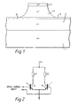
- an n-p-n transistor in accordance with the invention comprises an n+ doped substrate 1 on which an n ⁇ InP layer 2 is epitaxially grown.
- a layer of p-doped InGaAsP 3 is grown on the epitaxial layer 2.
- Another epitaxial layer of n ⁇ doped InP 4 is grown as a ridge on the p-doped layer 3.
- An n+ doped capping layer 5 is laid down on top of the epitaxial layer 4. The emitter contact of the transistor is made via the capping layer 5 and the collector contact through the substrate 1.
- the base contact is made to the p-doped layer 3.
- any light transmitted along the InGaAsP layer 3 is substantially confined by the vertical refractive index difference in the region of the ridge.
- the ridge also defines the lateral confinement of the light.
- Current injected via the base contact controls the electric field in the region of the ridge 4 and hence the refractive index of the layer 3 by means of the Pockels effect, Kerr effect and by current injection/depletion. This enables the passage of light transmitted along the waveguide to be controlled.
- the mode velocity in the waveguide may be controlled. It is possible to achieve relatively large changes in the phase of light transmitted through the device.
- the device may be arranged to be optically triggered.
- two devices 6 and 7 similar to that illustrated in Figure 1 are arranged as a long-tailed pair in which their emitters 8 and 9 are connected.
- the devices 6 and 7 may be formed on the same substrate and their optical waveguides coupled. The arrangement enables high switching speeds and a digital-type response to be achieved. lt also may give enhanced non-linearity for optical/optical switching where desired.
- the emitter contact is made through the substrate and the capping layer of the devices acts as the collector contact. This is particularly advantageous in the long-tailed pair arrangement.
Landscapes
- Physics & Mathematics (AREA)
- Nonlinear Science (AREA)
- General Physics & Mathematics (AREA)
- Optics & Photonics (AREA)
- Optical Integrated Circuits (AREA)
- Light Receiving Elements (AREA)
- Optical Modulation, Optical Deflection, Nonlinear Optics, Optical Demodulation, Optical Logic Elements (AREA)
- Bipolar Transistors (AREA)
Applications Claiming Priority (2)
| Application Number | Priority Date | Filing Date | Title |
|---|---|---|---|
| GB8814365 | 1988-06-16 | ||
| GB888814365A GB8814365D0 (en) | 1988-06-16 | 1988-06-16 | Optical devices |
Publications (2)
| Publication Number | Publication Date |
|---|---|
| EP0347232A2 true EP0347232A2 (de) | 1989-12-20 |
| EP0347232A3 EP0347232A3 (de) | 1991-05-22 |
Family
ID=10638831
Family Applications (1)
| Application Number | Title | Priority Date | Filing Date |
|---|---|---|---|
| EP19890306095 Withdrawn EP0347232A3 (de) | 1988-06-16 | 1989-06-15 | Optische Vorrichtungen |
Country Status (3)
| Country | Link |
|---|---|
| US (1) | US5028108A (de) |
| EP (1) | EP0347232A3 (de) |
| GB (2) | GB8814365D0 (de) |
Cited By (1)
| Publication number | Priority date | Publication date | Assignee | Title |
|---|---|---|---|---|
| FR2663161A1 (fr) * | 1990-06-08 | 1991-12-13 | Thomson Csf | Guide d'onde optique a structure de transistor integre et applications a la realisation de modulateurs de lasers et de coupleurs optique. |
Families Citing this family (3)
| Publication number | Priority date | Publication date | Assignee | Title |
|---|---|---|---|---|
| US5140652A (en) * | 1988-05-30 | 1992-08-18 | Koninklijke Ptt Netherland N.V. | Electro-optical component and method for making the same |
| GB2230616B (en) * | 1989-03-30 | 1993-07-14 | British Telecomm | Silicon bipolar phase modulator |
| US5732179A (en) * | 1995-03-30 | 1998-03-24 | Bell Communications Research, Inc. | Birefringence-free semiconductor waveguide |
Family Cites Families (9)
| Publication number | Priority date | Publication date | Assignee | Title |
|---|---|---|---|---|
| US4093345A (en) * | 1976-05-27 | 1978-06-06 | Bell Telephone Laboratories, Incorporated | Semiconductor rib waveguide optical modulator with heterojunction control electrode cladding |
| US4382660A (en) * | 1976-06-16 | 1983-05-10 | Massachusetts Institute Of Technology | Optical transistors and logic circuits embodying the same |
| US4378629A (en) * | 1979-08-10 | 1983-04-05 | Massachusetts Institute Of Technology | Semiconductor embedded layer technology including permeable base transistor, fabrication method |
| US4388633A (en) * | 1980-09-29 | 1983-06-14 | Hughes Aircraft Company | Monolithic transistor coupled electroluminescent diode |
| US4518934A (en) * | 1982-02-16 | 1985-05-21 | At&T Bell Laboratories | Optical bistable device |
| US4716449A (en) * | 1984-03-14 | 1987-12-29 | American Telephone And Telegraph Company At&T Bell Laboratories | Nonlinear and bistable optical device |
| US4706103A (en) * | 1985-06-17 | 1987-11-10 | Hughes Aircraft Company | Bipolar electrode scheme for electro-optic semiconductor waveguide devices |
| JPH06101557B2 (ja) * | 1986-09-19 | 1994-12-12 | 松下電器産業株式会社 | 光集積回路 |
| JPH0721594B2 (ja) * | 1987-01-19 | 1995-03-08 | 国際電信電話株式会社 | 光スイツチ |
-
1988
- 1988-06-16 GB GB888814365A patent/GB8814365D0/en active Pending
-
1989
- 1989-06-15 EP EP19890306095 patent/EP0347232A3/de not_active Withdrawn
- 1989-06-15 US US07/366,129 patent/US5028108A/en not_active Expired - Fee Related
- 1989-06-15 GB GB8913751A patent/GB2221768B/en not_active Expired - Lifetime
Non-Patent Citations (3)
| Title |
|---|
| APPLIED PHYSICS LETTERS, vol. 50, no. 12, March 1987, pages 708-710; A. KASTALSKY et al.: "Novel optoelectronic single quantum well devices based on electron bleaching of exciton absorption" * |
| IEEE ELECTRON DEVICE LETTERS, vol. 7, no. 11, November 1986, pages 605-606; K. TADA et al.: "Bipolar transistor carrier-injected optical modulator/switch: Proposal and analysis" * |
| IEEE JOURNAL OF QUANTUM ELECTRONICS, vol. 25, no. 4, April 1989, pages 713-719; Y. OKADA et al.: "The effect of band-tails on the design of GaAs/AlGaAs bipolar transistor carrier-injected optical modulator/switch" * |
Cited By (1)
| Publication number | Priority date | Publication date | Assignee | Title |
|---|---|---|---|---|
| FR2663161A1 (fr) * | 1990-06-08 | 1991-12-13 | Thomson Csf | Guide d'onde optique a structure de transistor integre et applications a la realisation de modulateurs de lasers et de coupleurs optique. |
Also Published As
| Publication number | Publication date |
|---|---|
| GB2221768A (en) | 1990-02-14 |
| US5028108A (en) | 1991-07-02 |
| EP0347232A3 (de) | 1991-05-22 |
| GB8814365D0 (en) | 1988-07-20 |
| GB2221768B (en) | 1992-09-09 |
| GB8913751D0 (en) | 1989-08-02 |
Similar Documents
| Publication | Publication Date | Title |
|---|---|---|
| Jones et al. | Heterogeneously integrated InP\/silicon photonics: fabricating fully functional transceivers | |
| JP2681044B2 (ja) | 光変調器 | |
| US5367582A (en) | Vertically-coupled arrow modulators or switches on silicon | |
| CN101133355B (zh) | 半导体光调制器 | |
| US4958898A (en) | Silicon double-injection electro-optic modulator with insulated-gate and method of using same | |
| US8488917B2 (en) | Electro-optic modulator | |
| US5285507A (en) | Controllable polarisation transformer | |
| US20170082876A1 (en) | Detector remodulator | |
| GB2523383A (en) | Detector remodulator | |
| CN103119804A (zh) | 损耗调制式硅倏逝波激光器 | |
| US7239762B2 (en) | Light modulation using the Franz-Keldysh effect | |
| Cavailles et al. | First digital optical switch based on InP/GaInAsP double heterostructure waveguides | |
| US5028108A (en) | Bipolar transistor including optical waveguide | |
| US7826688B1 (en) | Enhancing the sensitivity of resonant optical modulating and switching devices | |
| GB2243241A (en) | Heterojunction bipolar transistor and optical waveguide device for monolithic integration | |
| US20030128415A1 (en) | Mach-zehnder modulator with individually optimized couplers for optical splitting at the input and optical combining at the output | |
| Montgomery et al. | 10 Gbit/s AlGaAs/GaAs HBT driver IC for lasers or lightwave modulators | |
| US10768454B2 (en) | Athermal modulator-switch with two superimposed rings | |
| TAKEUCHI et al. | Low switching voltage InGaAsP/InP wave-guide interferometric modulator for integrated optics | |
| Yasaka et al. | Improvement in bandwidth of an electro-absorption modulator by optical pre-emphasis utilizing photon-photon resonance | |
| Jager et al. | Travelling-wave optoelectronic devices for microwave applications | |
| Zucker | High‐speed quantum‐well interferometric modulators for InP‐based photonic integrated circuits | |
| US20050002597A1 (en) | Integrated optical router and wavelength convertor matrix | |
| Irace et al. | High-efficiency silicon optoelectronic modulator based on a Bragg mirror and integrated in a low-loss silicon-on-insulator waveguide | |
| Zucker | Quantum-well electrorefraction and optical waveguide device applications |
Legal Events
| Date | Code | Title | Description |
|---|---|---|---|
| PUAI | Public reference made under article 153(3) epc to a published international application that has entered the european phase |
Free format text: ORIGINAL CODE: 0009012 |
|
| AK | Designated contracting states |
Kind code of ref document: A2 Designated state(s): DE FR IT NL SE |
|
| PUAL | Search report despatched |
Free format text: ORIGINAL CODE: 0009013 |
|
| AK | Designated contracting states |
Kind code of ref document: A3 Designated state(s): DE FR IT NL SE |
|
| STAA | Information on the status of an ep patent application or granted ep patent |
Free format text: STATUS: THE APPLICATION IS DEEMED TO BE WITHDRAWN |
|
| 18D | Application deemed to be withdrawn |
Effective date: 19920102 |