EP0347233A2 - Anordnung integrierter Optik - Google Patents
Anordnung integrierter Optik Download PDFInfo
- Publication number
- EP0347233A2 EP0347233A2 EP89306096A EP89306096A EP0347233A2 EP 0347233 A2 EP0347233 A2 EP 0347233A2 EP 89306096 A EP89306096 A EP 89306096A EP 89306096 A EP89306096 A EP 89306096A EP 0347233 A2 EP0347233 A2 EP 0347233A2
- Authority
- EP
- European Patent Office
- Prior art keywords
- section
- waveguide
- bend
- adjacent
- parts
- Prior art date
- Legal status (The legal status is an assumption and is not a legal conclusion. Google has not performed a legal analysis and makes no representation as to the accuracy of the status listed.)
- Withdrawn
Links
- 230000003287 optical effect Effects 0.000 claims description 9
- 230000007704 transition Effects 0.000 claims description 9
- 238000000034 method Methods 0.000 description 3
- 239000000758 substrate Substances 0.000 description 3
- 238000005452 bending Methods 0.000 description 2
- 230000002459 sustained effect Effects 0.000 description 2
- 230000000694 effects Effects 0.000 description 1
- 238000012856 packing Methods 0.000 description 1
- 239000004065 semiconductor Substances 0.000 description 1
Images


Classifications
-
- G—PHYSICS
- G02—OPTICS
- G02B—OPTICAL ELEMENTS, SYSTEMS OR APPARATUS
- G02B6/00—Light guides; Structural details of arrangements comprising light guides and other optical elements, e.g. couplings
- G02B6/10—Light guides; Structural details of arrangements comprising light guides and other optical elements, e.g. couplings of the optical waveguide type
- G02B6/12—Light guides; Structural details of arrangements comprising light guides and other optical elements, e.g. couplings of the optical waveguide type of the integrated circuit kind
- G02B6/122—Basic optical elements, e.g. light-guiding paths
- G02B6/125—Bends, branchings or intersections
Definitions
- This invention relates to integrated optic devices and more particularly to those devices which include an optical waveguide having a bend.
- a fundamental consideration in the design of integrated optical circuits is the packing density of components on a substrate. This is limited principally by the angles through which waveguides may be turned in order to access each component. In presently known semiconductor optical circuits, much of the substrate area is taken up with waveguides fanning into and out of devices, or clusters of devices, at low angles, typically about 1 degree.
- the present invention arose in an attempt to provide a waveguide structure capable of handling large angle bends without unacceptable power losses.
- an integrated optic device comprising an optical waveguide having a bend and a waveguide section at the bend capable of supporting more than one waveguide mode at the operating frequency.
- the waveguide is substantially symmetrical in configuration about the bend in the region of the bend.
- the parts of the waveguide adjacent to the section are then inclined with respect to that section by the same amount, such that if, for example, a total bend angle of 6 o required, there is a 3 o angle between each of the adjacent parts and the section.
- a total bend angle of 6 o required, there is a 3 o angle between each of the adjacent parts and the section.
- the dimensions of the waveguide are arranged such that the amount of optical power transmitted in each mode of the section is substantially equal. It is believed that, when this condition is fulfilled, the cleanest interchange of energy from one side of the section to the other will occur. Both symmetric and antisymmetric modes may be present, and it is desirable that the power transmitted in each mode is substantially the same.
- the centre line of a portion of the waveguide adjacent the section is offset from the centre line of the section.
- the outer bound of the section is curved. This enables a relatively smooth transition to be obtained between the section and adjoining portions of the waveguide so that there is no discontinuity of slope on the outer bound of the waveguide at the bend.
- the inner bound of the section may also be curved.
- the refractive index within the section is greater than that of parts of the waveguide adjacent to it.
- the section may be made to support a plurality of modes whereas the adjacent parts are monomode.
- the section may have more than one index value or there could be a continuous gradient change in refractive index within the section.
- the waveguide may be of uniform width, this being particularly convenient where it is wished to minimize the area of a device occupied by optical waveguides.
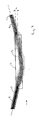
- an integrated optic device has a substrate of InP and includes a waveguide 4 of InGaAsP having a bi-moded section 5 and adjacent waveguide portions 6 and 7 which are inclined relative to the section 5 to give a total bend angle of 6 o .
- the inner and outer bounds of the waveguide are stepped where the section 5 and adjacent portions 6 and 7 of the waveguide meet.
- the centre-lines of the section 5 and portions 6 and 7 are indicated by broken lines. It can be seen that, in this embodiment, the centre lines of portions 6 and 7 are not offset from the centre line of section 5 at the ends of that section.
- the wavelength of light transmitted along the waveguide is 1.55 microns and the width of the lead-in and lead-out portions 6 and 7 is of the order of 2 microns.
- the bi-moded section 5 is between about 150 and 200 microns long and has a width of about 4 microns. This arrangement has losses which are reduced compared to those of previously known structures.
- Figure 3 illustrates another embodiment of the invention, in which there is a smooth transition between the inner bounds 8 and 9 of the lead-in and lead-out portions 10 and 11 and the inner bound 12 of adjacent a bi-moded section 13, the outer bounds being stepped.
- the centre lines of portions 10 and 11 are offset from the centre line of section 13 by an amount a .
- the dimensions of the portions 10 and 11 and the section 13 are the same as those of the arrangement illustrated in Figure 2 except that the section 13 is somewhat longer. In this case, it was found that an offset of about 1 micron produced mode powers differing by only a small amount, giving a geometry having low losses for a total bend angle of 6 o .
- a multi-moded section 14 and adjacent lead-in and lead-out portions 15 and 16 are such that there is a smooth transition between the inner and outer bounds of the section 14 and adjacent portions 15 and 16. This is a particularly advantageous structure, having low losses.
- Figure 5 shows another structure in which there is a smooth transition between the inner and outer bounds of different parts of the waveguide.
- the outer bound is curved to eliminate the discontinuity of slope present in the structure illustrated in Figure 4.
- the maximum width of the bi-moded section 17 is about a micron larger than the widths of the sections shown in Figures 2 to 4 and again this structure exhibits particularly low power losses at the bend.
- another device includes a waveguide 18 which comprises a multi-moded section 19, the outer and inner bounds 20 and 21 of which are both curved the radius of curvature of the outer bound 20 being smaller than that of the inner bound 21.
- a multi-moded section 22 is located at a bend in a waveguide 23.
- the width of the section 22 and the rest of the waveguide 23 is substantially the same, the multi-moded capability of the section 22 being achieved by increasing its refractive index compared to that of adjacent parts of the waveguide.
Landscapes
- Physics & Mathematics (AREA)
- Engineering & Computer Science (AREA)
- Microelectronics & Electronic Packaging (AREA)
- General Physics & Mathematics (AREA)
- Optics & Photonics (AREA)
- Optical Integrated Circuits (AREA)
Applications Claiming Priority (4)
| Application Number | Priority Date | Filing Date | Title |
|---|---|---|---|
| GB888814366A GB8814366D0 (en) | 1988-06-16 | 1988-06-16 | Integrated optic devices |
| GB8814366 | 1988-06-16 | ||
| GB8818911A GB2219871B (en) | 1988-06-16 | 1988-08-09 | Integrated optic devices |
| GB8818911 | 1988-08-09 |
Publications (2)
| Publication Number | Publication Date |
|---|---|
| EP0347233A2 true EP0347233A2 (de) | 1989-12-20 |
| EP0347233A3 EP0347233A3 (de) | 1991-02-13 |
Family
ID=26294037
Family Applications (1)
| Application Number | Title | Priority Date | Filing Date |
|---|---|---|---|
| EP19890306096 Withdrawn EP0347233A3 (de) | 1988-06-16 | 1989-06-15 | Anordnung integrierter Optik |
Country Status (2)
| Country | Link |
|---|---|
| US (1) | US4993794A (de) |
| EP (1) | EP0347233A3 (de) |
Cited By (3)
| Publication number | Priority date | Publication date | Assignee | Title |
|---|---|---|---|---|
| FR2715232A1 (fr) * | 1994-01-19 | 1995-07-21 | Commissariat Energie Atomique | Procédé d'optimisation d'un trajet d'un guide optique et guide optique obtenu par ce procédé. |
| EP0880037A3 (de) * | 1997-05-21 | 2000-08-02 | Nec Corporation | Wellenleiterelement, Wellenleiterverzweigung oder Kopplerelement und integrierter Wellenleiterschaltkreis |
| US6243525B1 (en) | 1998-02-13 | 2001-06-05 | Jds Uniphase Photonics C.V. | Optical waveguide device comprising at least one bent waveguide channel |
Families Citing this family (2)
| Publication number | Priority date | Publication date | Assignee | Title |
|---|---|---|---|---|
| EP0549332B1 (de) * | 1991-12-24 | 1999-03-17 | The Whitaker Corporation | Optisches Kopplungselement |
| US5243672A (en) * | 1992-08-04 | 1993-09-07 | At&T Bell Laboratories | Planar waveguide having optimized bend |
Family Cites Families (7)
| Publication number | Priority date | Publication date | Assignee | Title |
|---|---|---|---|---|
| US4015893A (en) * | 1972-10-12 | 1977-04-05 | Kentaro Hayashi, President, University of Tokyo | Compound semiconductor optical integrated circuit having isolation zones for light transmission |
| DE3107112C2 (de) * | 1981-02-26 | 1985-09-05 | Philips Kommunikations Industrie AG, 8500 Nürnberg | Dielektrische Leitung |
| US4376138A (en) * | 1982-01-04 | 1983-03-08 | Bell Telephone Laboratories, Incorporated | Optical waveguides in InGaAsP and InP |
| US4695121A (en) * | 1985-01-28 | 1987-09-22 | Polaroid Corporation | Integrated optic resonant structres and fabrication method |
| GB8610227D0 (en) * | 1986-04-25 | 1986-05-29 | Plessey Co Plc | Organic optical waveguides |
| US4810049A (en) * | 1987-04-02 | 1989-03-07 | American Telephone And Telegraph Company, At&T Bell Laboratories | Reducing bend and coupling losses in integrated optical waveguides |
| EP0365724A1 (de) * | 1988-10-26 | 1990-05-02 | THE GENERAL ELECTRIC COMPANY, p.l.c. | Integrierte optische Wellenleiterkrümmung |
-
1989
- 1989-06-15 EP EP19890306096 patent/EP0347233A3/de not_active Withdrawn
- 1989-08-18 US US07/395,456 patent/US4993794A/en not_active Expired - Fee Related
Cited By (5)
| Publication number | Priority date | Publication date | Assignee | Title |
|---|---|---|---|---|
| FR2715232A1 (fr) * | 1994-01-19 | 1995-07-21 | Commissariat Energie Atomique | Procédé d'optimisation d'un trajet d'un guide optique et guide optique obtenu par ce procédé. |
| EP0668517A1 (de) * | 1994-01-19 | 1995-08-23 | Commissariat A L'energie Atomique | Verfahren zur Optimierung der Wellenleiterform und durch dieses Verfahren gewonnener Wellenleiter |
| US5524165A (en) * | 1994-01-19 | 1996-06-04 | Commissariat A L'energie Atomique | Method for optimizing a path length of an optical guide and optical guide obtained by said method |
| EP0880037A3 (de) * | 1997-05-21 | 2000-08-02 | Nec Corporation | Wellenleiterelement, Wellenleiterverzweigung oder Kopplerelement und integrierter Wellenleiterschaltkreis |
| US6243525B1 (en) | 1998-02-13 | 2001-06-05 | Jds Uniphase Photonics C.V. | Optical waveguide device comprising at least one bent waveguide channel |
Also Published As
| Publication number | Publication date |
|---|---|
| EP0347233A3 (de) | 1991-02-13 |
| US4993794A (en) | 1991-02-19 |
Similar Documents
| Publication | Publication Date | Title |
|---|---|---|
| Meade et al. | Novel applications of photonic band gap materials: Low‐loss bends and high Q cavities | |
| US4678267A (en) | Parabolic optical waveguide horns and design thereof | |
| JP2537800Y2 (ja) | インテグレイテッド光導波路 | |
| JP3153120B2 (ja) | テーパ状導波路 | |
| US5729643A (en) | Tapered composite optical fiber and method of making the same | |
| US3712705A (en) | Air clad optical fiber waveguide | |
| JP5082414B2 (ja) | 光半導体装置および光導波路装置 | |
| EP3446164B1 (de) | Optischer wellenleiterabschluss mit dotierter, lichtabsorbierender platte | |
| US8649645B2 (en) | Optical waveguide and a method of fabricating an optical waveguide | |
| EP0731367B1 (de) | Integriert optischer Wellenleiter mit seitlichen Lücken zunehmender Tiefe zur Modenanpassung an einer Faser | |
| US4906062A (en) | Integrated optical waveguide bend | |
| US6028973A (en) | Arrangement of two integrated optical waveguides on the surface of a substrate | |
| JP2004503800A (ja) | 低インデックス差導波路と高インデックス差導波路との間に設けられるモード変成器 | |
| JP2000507712A (ja) | 光集積化ビーム拡がりトランスフォーマ | |
| JP4012367B2 (ja) | 単一モード光ウェーブガイド結合要素 | |
| EP0220315B1 (de) | Geräte mit optischen wellenleitern und mit niedrigen verlusten | |
| WO2021015981A1 (en) | Multi-pass free-carrier absorption variable optical attenuators and multi-pass thermal phase shifters | |
| US4993794A (en) | Integrated optic waveguide with bend | |
| JPH1054915A (ja) | 光分岐素子 | |
| JP2000258648A (ja) | 光平面導波路 | |
| GB2219871A (en) | Integrated optic device having an optical waveguide bend | |
| JPH08160233A (ja) | 集積光学素子 | |
| US4988156A (en) | Bent waveguide for an optical integrated circuit | |
| US20230418092A1 (en) | Thermo-optical phase shifter | |
| WO2004021056A1 (en) | Improved photonic crystal device |
Legal Events
| Date | Code | Title | Description |
|---|---|---|---|
| PUAI | Public reference made under article 153(3) epc to a published international application that has entered the european phase |
Free format text: ORIGINAL CODE: 0009012 |
|
| AK | Designated contracting states |
Kind code of ref document: A2 Designated state(s): DE FR IT NL SE |
|
| PUAL | Search report despatched |
Free format text: ORIGINAL CODE: 0009013 |
|
| AK | Designated contracting states |
Kind code of ref document: A3 Designated state(s): DE FR IT NL SE |
|
| 17P | Request for examination filed |
Effective date: 19910425 |
|
| STAA | Information on the status of an ep patent application or granted ep patent |
Free format text: STATUS: THE APPLICATION IS DEEMED TO BE WITHDRAWN |
|
| 18D | Application deemed to be withdrawn |
Effective date: 19930101 |