EP0347541A1 - Procédé de modulation numérique de phase d'une porteuse par des signaux de données et modulateur numérique de phase pour la mise en oeuvre de ce procédé - Google Patents
Procédé de modulation numérique de phase d'une porteuse par des signaux de données et modulateur numérique de phase pour la mise en oeuvre de ce procédé Download PDFInfo
- Publication number
- EP0347541A1 EP0347541A1 EP89106762A EP89106762A EP0347541A1 EP 0347541 A1 EP0347541 A1 EP 0347541A1 EP 89106762 A EP89106762 A EP 89106762A EP 89106762 A EP89106762 A EP 89106762A EP 0347541 A1 EP0347541 A1 EP 0347541A1
- Authority
- EP
- European Patent Office
- Prior art keywords
- digital
- phase modulator
- data
- carrier
- phase
- Prior art date
- Legal status (The legal status is an assumption and is not a legal conclusion. Google has not performed a legal analysis and makes no representation as to the accuracy of the status listed.)
- Withdrawn
Links
- 238000000034 method Methods 0.000 title claims abstract description 49
- 230000006870 function Effects 0.000 claims abstract description 6
- 230000005540 biological transmission Effects 0.000 claims description 16
- 230000015654 memory Effects 0.000 claims description 16
- 238000006243 chemical reaction Methods 0.000 claims description 10
- 238000012546 transfer Methods 0.000 claims description 9
- 238000001914 filtration Methods 0.000 claims description 8
- 238000011144 upstream manufacturing Methods 0.000 claims description 7
- 238000012545 processing Methods 0.000 claims description 5
- 238000005516 engineering process Methods 0.000 claims description 4
- 238000007493 shaping process Methods 0.000 claims description 3
- 230000003595 spectral effect Effects 0.000 claims description 3
- 230000010355 oscillation Effects 0.000 abstract description 3
- 238000010586 diagram Methods 0.000 description 9
- 230000000694 effects Effects 0.000 description 3
- 230000010363 phase shift Effects 0.000 description 3
- 238000011161 development Methods 0.000 description 2
- 230000018109 developmental process Effects 0.000 description 2
- 238000012986 modification Methods 0.000 description 2
- 230000004048 modification Effects 0.000 description 2
- 230000000712 assembly Effects 0.000 description 1
- 238000000429 assembly Methods 0.000 description 1
- 230000015572 biosynthetic process Effects 0.000 description 1
- 230000000295 complement effect Effects 0.000 description 1
- 230000003111 delayed effect Effects 0.000 description 1
- 230000001419 dependent effect Effects 0.000 description 1
- 230000009760 functional impairment Effects 0.000 description 1
- 238000010438 heat treatment Methods 0.000 description 1
- 238000012544 monitoring process Methods 0.000 description 1
- 239000010453 quartz Substances 0.000 description 1
- 230000000630 rising effect Effects 0.000 description 1
- VYPSYNLAJGMNEJ-UHFFFAOYSA-N silicon dioxide Inorganic materials O=[Si]=O VYPSYNLAJGMNEJ-UHFFFAOYSA-N 0.000 description 1
- 230000002123 temporal effect Effects 0.000 description 1
Images

Classifications
-
- H—ELECTRICITY
- H04—ELECTRIC COMMUNICATION TECHNIQUE
- H04H—BROADCAST COMMUNICATION
- H04H20/00—Arrangements for broadcast or for distribution combined with broadcast
- H04H20/28—Arrangements for simultaneous broadcast of plural pieces of information
- H04H20/36—Arrangements for simultaneous broadcast of plural pieces of information for AM broadcasts
-
- H—ELECTRICITY
- H04—ELECTRIC COMMUNICATION TECHNIQUE
- H04L—TRANSMISSION OF DIGITAL INFORMATION, e.g. TELEGRAPHIC COMMUNICATION
- H04L27/00—Modulated-carrier systems
- H04L27/18—Phase-modulated carrier systems, i.e. using phase-shift keying
- H04L27/20—Modulator circuits; Transmitter circuits
- H04L27/2003—Modulator circuits; Transmitter circuits for continuous phase modulation
-
- H—ELECTRICITY
- H04—ELECTRIC COMMUNICATION TECHNIQUE
- H04L—TRANSMISSION OF DIGITAL INFORMATION, e.g. TELEGRAPHIC COMMUNICATION
- H04L27/00—Modulated-carrier systems
- H04L27/18—Phase-modulated carrier systems, i.e. using phase-shift keying
- H04L27/20—Modulator circuits; Transmitter circuits
- H04L27/2032—Modulator circuits; Transmitter circuits for discrete phase modulation, e.g. in which the phase of the carrier is modulated in a nominally instantaneous manner
- H04L27/2053—Modulator circuits; Transmitter circuits for discrete phase modulation, e.g. in which the phase of the carrier is modulated in a nominally instantaneous manner using more than one carrier, e.g. carriers with different phases
- H04L27/206—Modulator circuits; Transmitter circuits for discrete phase modulation, e.g. in which the phase of the carrier is modulated in a nominally instantaneous manner using more than one carrier, e.g. carriers with different phases using a pair of orthogonal carriers, e.g. quadrature carriers
- H04L27/2067—Modulator circuits; Transmitter circuits for discrete phase modulation, e.g. in which the phase of the carrier is modulated in a nominally instantaneous manner using more than one carrier, e.g. carriers with different phases using a pair of orthogonal carriers, e.g. quadrature carriers with more than two phase states
- H04L27/2071—Modulator circuits; Transmitter circuits for discrete phase modulation, e.g. in which the phase of the carrier is modulated in a nominally instantaneous manner using more than one carrier, e.g. carriers with different phases using a pair of orthogonal carriers, e.g. quadrature carriers with more than two phase states in which the data are represented by the carrier phase, e.g. systems with differential coding
Definitions
- the invention relates to a method for digital phase modulation of a carrier by data signals according to the preamble of claim 1 and a digital phase modulator for executing the method.
- a digital phase modulator for analog band-limited low frequency (LF) modulation signals is known, which works on the basis of the method described by Zinke / Brunswig.
- the known modulator consists of an in-phase and a quadrature branch, which are combined on the output side in an adder.
- the signals i (t) and q (t) then each pass through a scanning unit and an analog low-pass filter before they each modulate the amplitude of the carrier in an analog modulator.
- the carrier which is fed to the modulator in the quadrature branch is rotated in its phase by 90 ° with respect to the carrier which is fed to the modulator in the in-phase branch.
- Analogue-working PM methods were also proposed, in which the frequency of the carrier frequency oscillator is stabilized by a quartz or an atomic standard and is only modulated in phase, in contrast to the related frequency modulation (FM), in which the frequency of a freely oscillating one Oscillator is modulated.
- FM frequency modulation
- the phase can be modulated, for example, with the aid of a serrasoid modulator (cf. p. 343 in the "Textbook of High Frequency Technology" by Zinke / Brunswig cited at the beginning) or with the help of a first-order all-pass filter that contains an operational amplifier and a variable capacitance diode.
- a serrasoid modulator cf. p. 343 in the "Textbook of High Frequency Technology" by Zinke / Brunswig cited at the beginning
- a first-order all-pass filter that contains an operational amplifier and a variable capacitance diode.
- a disadvantage of the serrasoid modulator is that the phase-modulated carrier vibration is due to its meandering shape still has to be filtered later.
- a disadvantage of the all-pass filter modulator is that there are generally nonlinear distortions in the waveform of the transmitted data, which are caused both by the modulating capacitance variation diode and by an arctangent connection between the phase modulation and the time curve of the data form.
- a general disadvantage of analog solutions is that the circuits have to be adjusted and that this adjustment has to be carried out during operation under unfavorable circumstances due to drift effects (e.g. due to heating of the components).
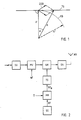
- the PM is shown in accordance with the pointer diagram (not drawn to scale) in FIG. 1 generated by vectorial addition of a double-sided modulation DSB rotated by 90 ° and a carrier of constant amplitude A 'not rotated in its phase.
- the amplitude A of the resulting, by the phase angle ⁇ deflected ("phase-modulated") carrier moves in this method with its tip on a straight line TG, which is perpendicular to the amplitude A 'of the unmodulated carrier and tangent to an arc KB, which through the Peak of the amplitude A ⁇ of an exactly phase-modulated carrier is described.
- this known PM method is only correct for very small phase strokes, namely only for the phase angle range in which the circular arc KB can be approximately replaced by the tangent straight line TG.
- this method results in an amplitude and a phase error due to the arc tangent curve, so that for this case, further side lines of a higher order are required for the exact description of the PM, the size of which is suitable for a sinusoidally modulated signal with the help of Bessel Functions.
- the PM method described basically opens up the possibility of being able to additionally transmit digital data in a simple manner in information transmission systems with an amplitude-modulated carrier by modulating the phase of the carrier.
- additional digital information in simplex traffic can be transmitted simultaneously and in a compatible (ie inaudible) manner to the normal radio program, such as. B. Traffic information.
- AM-RDS Such an AM radio data system
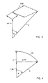
- the still unmodulated carrier RF of the control transmitter SS is modulated in its phase in a downstream phase modulator PM by means of a suitable PM method with the data D to be transmitted, and the now phase-modulated carrier RF ⁇ via a driver stage TS into the RF output stage AM of the transmitter is fed in and is modulated there in a known manner with the LF signal amplified by the modulation amplifier MV.
- the amplitude- and phase-modulated carrier is then fed to the antenna AN via an RF resonant circuit SK and transmitted.
- the transmitter obtains the required energy from the power supply SV.
- Such a modified AM radio broadcasting system is described for example in DE-OS 36 16 864.
- AM-RDS With AM-RDS, a simplex data channel can be implemented for the large-scale bridging of larger distances (even areas with little infrastructure), which can usually be implemented in existing transmitters without great difficulty (see: E. Augustin, R. Kuehne "A novel method for the additional, simultaneous and compatible transmission of digital information via an AM radio broadcasting system in simplex traffic", Technische Mitteilungen des RFZ, 30th year, volume 2, 1986, pages 25 to 30).
- the information transmitted via this simplex channel can be, for example: - coordination aids (program chain identifier, name of the program chain, program type, alternative frequencies, etc.), - Station characteristics e.g. B. for remote monitoring, - Traffic information, which may be structured or addressed regionally and which may be used as control commands for a receiver-side memory for information output or z. B. can be sent as plain text using a receiver-localized speech system, - weather service information, - alarm, call and security information, - switching signals (traffic announcement identification, decoder control, music / speech identification, program contribution identification etc.), - Time / frequency information, e.g. B. to control public master and slave clocks, - teletype information in point-to-area operation (simplex), - Telecontrol signals for special users with large-scale effects and fixed or mobile receiving points without a return channel.
- - coordination aids program chain identifier, name of the program chain, program type, alternative frequencies, etc.
- Traffic information which may be structured
- a major disadvantage of the known AM-RDS is that - That in the PM modulators used RC low-pass filters 2nd order, possibly 3rd order, are used for rounding the data to be transmitted, so that the data signals generally do not have an optimal time profile and cannot be limited to the theoretically necessary minimum bandwidth and thus connected, a comparatively small signal-to-noise ratio to the AM channel occurs, so that interference of the AM channel due to the additionally transmitted data cannot be excluded; - that analog filters have to be adjusted; - that there is no code conversion; - that no DC code is used; - That no clock information is contained in the data signal and therefore the "start-stop" method known from teletype is used, which does not allow optimal transmission speeds; - that there is no code protection against errors.
- the object of the invention is to provide a method of the type mentioned in the introduction with which the least possible distortion of the data signals to be transmitted is achieved becomes.
- the mutual interference of the data signals to be transmitted and the normal program should be as small as possible, ie the signal-to-noise ratio from the simplex data channel to the AM channel should be as large as possible.
- the basis of the digital phase modulation method according to the invention is a modified quadrature amplitude modulation method ("QAM").
- QAM quadrature amplitude modulation method
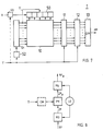
- This method continues according to FIG. 3 together from an amplitude modulation AM of the carrier and a double sideband modulation DSB rotated by 90 °.
- the AM and the DSB are designed so that the pointer A of the resulting PM both maintains a constant length and the time course of its oscillation, i.e. ⁇ (t), exactly matches the modulating signal.
- the two amplitude-modulated carrier amplitudes I ( ⁇ ) and Q ( ⁇ ) of the in-phase or quadrature branch rotated by 90 ° relative to one another, add up vectorially so that the pointer A with its resulting PM Tip oscillates back and forth on a circular arc KB.
- any phase shift can be implemented, but this is of no importance for the application of an AM-RDS considered here, since it has been shown in the case of data transmission in AM radio broadcasting that, for reasons of compatibility, only phase swings of a maximum of ⁇ 30 ° can be considered .
- phase modulation Since rounded data are to be transmitted with the phase modulation according to the invention, their time profiles and thus also the phase profiles of the PM have a well-defined form that can be easily calculated for all conceivable bit combinations.
- these time profiles for the AM signal and the DSB signal are therefore calculated beforehand and stored as reference values in a memory, for. B. an EPROM.
- the EPROMs are then read out in dependence on the data currently to be transmitted in such a way that there is a 90 ° rotation of the DSB signal relative to the AM signal.
- FM-RDS frequency-modulated transmitters in the FM range
- a double sideband signal at 57 kHz is required, in which the phase position of the (suppressed) carrier is rotated by 90 ° with respect to the traffic radio carrier at 57 kHz, the so-called ARI system (auto broadcast information system) is.
- the time course of this DSB is stored in a modulated and rounded form in a memory (EPROM) and is read out and sent out depending on the data signal to be transmitted.
- the generally non-band-limited digital data signals (e.g. NRZ signals: non-return-to-zero signals) are subjected to digital filtering beforehand in the method according to the invention for the purpose of spectral shaping and band limitation, the data to be filtered being before or during the digital filtering are made free of direct current by a code conversion and, if necessary, provided with the clock information required for further processing.
- NRZ signals non-return-to-zero signals
- the data signals in the method according to the invention are first divided into a sequence of words of a predetermined length with an odd number of bits.
- the time profile of the filtered word corresponding to the middle bit of the word is then calculated for each possible word and stored in the form of base values in an area addressed by the word in at least one memory.
- the currently applied (to be transmitted) word causes the area assigned to it in the at least one memory is selected and the base values stored in this area are read out synchronously with the frequency of the carrier.
- the previously calculated time profiles of the filtered words are advantageously weighted using a predetermined window function.
- the duration of the individual bits must be selected as an integral multiple of half the period of the carrier, so that the data transmission rate can be changed in stages according to this secondary condition, the unmodulated and / or the phase-modulated carrier can have a sinusoidal or rectangular time profile.
- FIG. 5 shows a block diagram of the digital phase modulator PM according to the invention for executing the digital PM method according to the invention.
- the data D to be transmitted first pass through a digital filter DF1 or DF2 in the in-phase branch 1 and in the quadrature branch 2 of the phase modulator PM and then through a modulator M1 or M2.
- the modulator M1 in the in-phase branch 1 together with the downstream adder A1, in which the carrier T is added, results in an AM modulator, at the output of which the amplitude-modulated carrier signal AM, which is not rotated in phase, is present.
- the modulator M2 delivers the phase rotated by 90 ° DSB signal, which is vectorially added in a second adder 3 with the amplitude-modulated carrier AM of the in-phase branch 1, so that the phase-modulated carrier T ⁇ appears at the output of the phase modulator.
- the carrier T also serves as a clock signal for the digital filters DF1 and DF2 and for the modulators M1 and M2.
- the 90 ° phase rotation of the DSB signal is accomplished with the aid of a digital 90 ° phase shifter 4, the 90 ° phase shift being produced in a known manner by dividing a faster clock with a rising or falling edge.
- FIG. 6 shows a more detailed block diagram of a preferred embodiment of the digital phase modulator PM according to the invention according to FIG. 5.
- In-phase and quadrature branches 1 and 2 are constructed with identical assemblies, specifically with memories in the form of EPROMs (or RAMs) 10 and 20, latches 11 and 21, switching modulators in the form of Ex-OR gates 12 or 22 and D / A converters 13 or 23, the RAMs taking over the base values from additional EPROMs in the initialization phase.
- the two branches 1 and 2 are brought together on the output side in the adder 3.
- a filter resonant circuit 6 and optionally an amplifier 7 are connected downstream of the adder 3.
- the EPROMs 10 and 20 are controlled via a common control 5, into which the data to be transmitted are fed.
- the clock information T for the individual modules are phase-shifted by 90 ° for the quadrature branch by means of a phase shifter 4.
- EPROMs 10 or 20 instead of 2 EPROMs 10 or 20, a single EPROM of the appropriate size can also be used, which is then to be operated in "multiplex mode" at twice the clock rate.
- FIG. 7 shows a detailed section of the embodiment of the digital phase modulator PM according to FIG. 6, which shows the in-phase branch 1 by way of example (as already mentioned, the quadrature branch has the same structure).
- 10 again denotes the EPROM (or RAM), 11 the latch, 12 the switching modulator and 13 the D / A converter.
- the control circuit 5 consists of a shift register 50, a primary divider 51 and possibly a prescaler 52 and optionally a code converter 53 for generating a DC component-free, ie. H. Line codes free of direct current and provided with sufficient clock information.
- T the system clock (z. B. the carrier frequency or, as discussed below, advantageously the same for all carrier frequencies subcarrier frequency) and with T 'the data clock is designated.
- the base values of the rounded curve shape represent the middle bit.
- this curve shape all pre- and post-oscillators of the rounded shape of the two leading and trailing bits are taken into account. This enables the optimal time delay according to the theory runs with z. B. to generate a predetermined bandwidth.
- symmetrical shapes can be obtained for the rounded data pulses.
- the associated rounded waveforms can be stored directly in the EPROMs of the in-phase or quadrature branch.
- the output signal of the code converter then again consists of a signal in NRZ format, but with a higher clock speed, inserted clock information and freedom from DC components (the latter also expressed as: running digital sum ⁇ ).
- the curve shapes belonging to rounded NRZ data are then in the "filter” EPROMs 10 and 20. The clock speed and the readout speed must be adjusted accordingly.
- the digital filtering of the data to be transmitted ie the data rounding and possibly code conversion (for example with NRZ data signals), is carried out with the aid of previously calculated and in the two EPROMs 10 and 20 stored base values.
- the digitally modulated signals are then converted in the D / A converters 13 and 23 into analog (quantized) AM or DSB signals which are shifted in phase by 90 ° and which are added in an analog manner in the adder 3 will.
- the downstream filter resonant circuit 6, whose resonance frequency corresponds to the center frequency of the PM, is used to smooth the resulting phase-modulated carrier oscillation, which is still present in a quantized, stepped form.
- the signal is further processed in the amplifier 7, which may be connected downstream.
- the system clock could be the carrier frequency T and, for an AM-RDS for long wave, would be supplied directly by the control transmitter, for example.
- an intermediate frequency IF as the system clock instead of the carrier frequency, since the data transmission rate R can thus be selected independently of the frequency of the carrier T.
- FIG. 7 A realization of this advantageous solution for AM-RDS is shown in FIG. 7 shown.
- a mixer M3 By mixing the still unmodulated Carrier frequency RF with the frequency of a fixed frequency oscillator LO ("Local Oscillator") in a mixer M3 generates an unmodulated intermediate frequency ZF, which serves as the system clock for the downstream phase modulator PM according to the invention and with the data to be transmitted D, which may first be used for the phase modulator PM go through upstream external code converter CW, phase modulated.
- the phase-modulated intermediate frequency signal ZF ⁇ is then mixed in a further mixer M4 with the same LO frequency, so that the desired phase-modulated carrier frequency RF ⁇ is present at the output of the mixer M4, which can then be further processed in a manner known per se (see FIG. 2).
- the waveforms of the rounded data signals are stored in the form of base values in the two EPROMs (both for the AM signals to be generated and for the DSB signals).
- the EPROMs can be replaced by fast RAMs.
- the RAMs are loaded in the initialization phase of the modulator by the values stored in the EPROMs. In principle, there is no difference. Therefore, only EPROMs are mentioned in the rest of the text.
- These base values are determined beforehand with the computer. Since the data to be transmitted can only be 0 or 1, the base values can be easily calculated in advance.
- the base values in the EPROMs do not deliberately result in the phase-modulated signal (which of course would alternatively be quite simple by storing the base values alternately (+/-)).
- the modulation takes place here in the two branches by means of additional Ex-OR switches in front of the A / D converters.
- the advantage of this measure is that the data transfer rate R, which corresponds to the read clock for the EPROMs, can be selected almost independently of the switching frequency, which is the same as the center frequency of the PM.
- the data clock (T 'in FIG. 7) should be an integer multiple of the switching or system clock.
- the modulation in the quadrature branch (2 in FIG. 6) takes place in the exemplary embodiments in FIGS. 6 and 7 by latching with a system clock offset by half a clock (T in FIG. 7), so that the required 90 ° phase rotation only occurs in the latch (22 in FIG. 6) of the quadrature branch.
- quadrature branch EPROM could be used Control directly with the system clock rotated by 90 °. To do this, the data arriving here might have to be delayed by half a system cycle.
- the factor 2 N is required so that by storing the base values in an EPROM, the EPROMs can be timed for the addresses in powers of 2, so that the individual base values advantageously all have the same width.
- the data transfer rate is dependent on the selected (intermediate) carrier frequency and can be varied within reasonable limits by choosing a suitable prescaler.
- the data (clock synchronously with the data clock T 'in FIG. 7) are generally provided in the NRZ format.
- the biphase code is free of direct components and has a maximum of clock information, namely one clock edge per bit.
- the disadvantage is the double bandwidth required compared to NRZ.
- Line codes Various other direct component-free codes provided with clock information (“line codes”) are known from the literature.
- B. be used in the magnetic storage of data such.
- QP Quadrature phase according to Bixly and Ketcham
- ZM Zero Modulation according to Patel
- Group codes e.g. E.g .: 5B / 6B or block codes
- the code conversion NRZ ⁇ Biphase can be carried out directly in the EPROMs, since only the associated rounded curve shapes have to be written.
- the other DC-free codes always require several bits to decide what the next bit must be so that the DC component disappears.
- An additional upstream code converter is therefore required, which in turn is also implemented as an EPROM or PAL.
- the data read out from the code converter are again in NRZ format, but with a faster cycle.
- a curve shape must then be stored in the "filter” EPROMs, which corresponds to the filtering of NRZ signals.
- the system clock should be chosen appropriately.
- the structure chosen for the digital phase modulator can also be used for a quadrature DSB modulator, which is often incorrectly referred to in the literature as a 4PSK modulator (4 PSK: phase shift keying with four states 0 °, 90 °, 180 °, 270 °).
- PSK phase shift keying with four states 0 °, 90 °, 180 °, 270 °.
- the following, essentially software-related changes are necessary for this: - In the in-phase and in the quadrature branch, the curve shapes must be stored for one rounded DSB shape (ie both branches are identical except for the 90 ° rotation). - In addition to the tasks required for the phase modulator, the code converter must also convert the bit stream into two di-bit streams. This means that the in-phase branch and the quadrature branch are modulated by different bit streams.
Landscapes
- Engineering & Computer Science (AREA)
- Signal Processing (AREA)
- Computer Networks & Wireless Communication (AREA)
- Digital Transmission Methods That Use Modulated Carrier Waves (AREA)
Applications Claiming Priority (2)
| Application Number | Priority Date | Filing Date | Title |
|---|---|---|---|
| DE3821014 | 1988-06-22 | ||
| DE19883821014 DE3821014A1 (de) | 1988-06-22 | 1988-06-22 | Verfahren zur digitalen phasenmodulation eines traegers durch datensignale und digitaler phasenmodulator zum ausfuehren des verfahrens |
Publications (1)
| Publication Number | Publication Date |
|---|---|
| EP0347541A1 true EP0347541A1 (fr) | 1989-12-27 |
Family
ID=6356977
Family Applications (1)
| Application Number | Title | Priority Date | Filing Date |
|---|---|---|---|
| EP89106762A Withdrawn EP0347541A1 (fr) | 1988-06-22 | 1989-04-15 | Procédé de modulation numérique de phase d'une porteuse par des signaux de données et modulateur numérique de phase pour la mise en oeuvre de ce procédé |
Country Status (2)
| Country | Link |
|---|---|
| EP (1) | EP0347541A1 (fr) |
| DE (1) | DE3821014A1 (fr) |
Cited By (5)
| Publication number | Priority date | Publication date | Assignee | Title |
|---|---|---|---|---|
| EP0489281A3 (en) * | 1990-12-06 | 1993-05-12 | Telefunken Sendertechnik Gmbh | Arrangement for signal processing in the modulation path to a transmitter |
| FR2709219A1 (fr) * | 1993-08-20 | 1995-02-24 | Feuillee Michel | Dispositif de programmation et de commande d'enregistrement d'émissions audio et/ou vidéo à partir de données diffusées. |
| WO1997001894A1 (fr) * | 1995-06-28 | 1997-01-16 | Deutsche Telekom Ag | Procede et circuit de modulation pour transmettre des signaux de donnees |
| WO1997039538A1 (fr) * | 1996-04-15 | 1997-10-23 | Info Telecom | Recepteur d'informations interactif, en particulier poste radiophonique interactif, et procede correspondant de transmission interactive d'informations |
| CN118508966A (zh) * | 2024-04-24 | 2024-08-16 | 电子科技大学 | 一种应用于逐次逼近型模数转换器的时钟控制比较器 |
Families Citing this family (2)
| Publication number | Priority date | Publication date | Assignee | Title |
|---|---|---|---|---|
| DE4027703A1 (de) * | 1990-08-31 | 1992-03-12 | Fraunhofer Ges Forschung | Integrierbarer schaltermodulator |
| DE19722913A1 (de) * | 1997-05-31 | 1998-12-03 | Alsthom Cge Alcatel | Gleitweg-Sendeeinrichtung für das Instrumentenlandesystem ILS |
Citations (4)
| Publication number | Priority date | Publication date | Assignee | Title |
|---|---|---|---|---|
| US4516087A (en) * | 1982-04-12 | 1985-05-07 | Rockwell International Corporation | Method for reducing side-lobe energy in an MSK detectable signal |
| WO1986003356A1 (fr) * | 1984-11-22 | 1986-06-05 | Devon County Council | Systeme modem de donnees |
| US4679238A (en) * | 1985-04-25 | 1987-07-07 | Blaupunkt Werke Gmbh | Method and system for signalling additional information by AM medium wave broadcasting |
| US4745628A (en) * | 1986-04-15 | 1988-05-17 | Terra Marine Engineering, Inc. | Symbol generator for phase modulated system |
-
1988
- 1988-06-22 DE DE19883821014 patent/DE3821014A1/de not_active Withdrawn
-
1989
- 1989-04-15 EP EP89106762A patent/EP0347541A1/fr not_active Withdrawn
Patent Citations (4)
| Publication number | Priority date | Publication date | Assignee | Title |
|---|---|---|---|---|
| US4516087A (en) * | 1982-04-12 | 1985-05-07 | Rockwell International Corporation | Method for reducing side-lobe energy in an MSK detectable signal |
| WO1986003356A1 (fr) * | 1984-11-22 | 1986-06-05 | Devon County Council | Systeme modem de donnees |
| US4679238A (en) * | 1985-04-25 | 1987-07-07 | Blaupunkt Werke Gmbh | Method and system for signalling additional information by AM medium wave broadcasting |
| US4745628A (en) * | 1986-04-15 | 1988-05-17 | Terra Marine Engineering, Inc. | Symbol generator for phase modulated system |
Non-Patent Citations (2)
| Title |
|---|
| INTERNATIONAL CONFERENCE ON COMMUNICATIONS, Washington, 7.-10. Juni 1987, Band 3, Seiten 39.3.1-39.3.5, IEEE, New York, US; S. YOSHIDA et al.: "Anti-multipath modulation technique - Machester-coded PSK (MC-PSK)" * |
| PATENT ABSTRACTS OF JAPAN, Band 10, nr. 251 (E-432)[2307], 28. August 1986, Seite 140 E 432; & JP-A-61 80 932 (NEC CORP.) 24-04-1986 * |
Cited By (7)
| Publication number | Priority date | Publication date | Assignee | Title |
|---|---|---|---|---|
| EP0489281A3 (en) * | 1990-12-06 | 1993-05-12 | Telefunken Sendertechnik Gmbh | Arrangement for signal processing in the modulation path to a transmitter |
| FR2709219A1 (fr) * | 1993-08-20 | 1995-02-24 | Feuillee Michel | Dispositif de programmation et de commande d'enregistrement d'émissions audio et/ou vidéo à partir de données diffusées. |
| WO1995006390A1 (fr) * | 1993-08-20 | 1995-03-02 | Michel Feuillee | Dispositif de programmation et de commande d'enregistrement |
| WO1997001894A1 (fr) * | 1995-06-28 | 1997-01-16 | Deutsche Telekom Ag | Procede et circuit de modulation pour transmettre des signaux de donnees |
| WO1997039538A1 (fr) * | 1996-04-15 | 1997-10-23 | Info Telecom | Recepteur d'informations interactif, en particulier poste radiophonique interactif, et procede correspondant de transmission interactive d'informations |
| CN118508966A (zh) * | 2024-04-24 | 2024-08-16 | 电子科技大学 | 一种应用于逐次逼近型模数转换器的时钟控制比较器 |
| CN118508966B (zh) * | 2024-04-24 | 2025-07-22 | 电子科技大学 | 一种应用于逐次逼近型模数转换器的时钟控制比较器 |
Also Published As
| Publication number | Publication date |
|---|---|
| DE3821014A1 (de) | 1989-12-28 |
Similar Documents
| Publication | Publication Date | Title |
|---|---|---|
| DE4191766C2 (de) | Frequenzsteuerschaltkreis für einen einstellbaren Empfänger-Oszillator | |
| DE3032749A1 (de) | Funkempfaenger | |
| DE69030402T2 (de) | System zur Unterbrechung der Ausgangswellen eines Senders | |
| DE2153376B2 (de) | Digitale nachrichtenuebertragungsanordnung | |
| DE2628581C3 (de) | Schaltung zur Wiedergewinnung von Taktsignalen mit veränderlicher Frequenz für einen Digitaldatenempfänger | |
| DE69228456T2 (de) | Basisband-Pulsumformer für GMSK-Modulatoren | |
| DE69215622T2 (de) | Zellulares Funkkommunikationssystem mit verschiedener Modulation abhängig von Zellgrösse | |
| DE69433255T2 (de) | Gruppen modulator | |
| EP0347541A1 (fr) | Procédé de modulation numérique de phase d'une porteuse par des signaux de données et modulateur numérique de phase pour la mise en oeuvre de ce procédé | |
| EP0200977B1 (fr) | Démodulateur numérique | |
| EP1317830B1 (fr) | Procede de production de signaux de communication mobile de differentes normes de telephonie mobile | |
| DE69935341T2 (de) | Rahmenformat für Funkkommunikationssystem | |
| DE3010565A1 (de) | Anordnung zum uebertragen digitaler daten | |
| DE68924332T2 (de) | Digitaler GMSK-Modulator mit nicht ganzzahliger Bitintervallverarbeitung. | |
| DE60202638T2 (de) | Verfahren zur Modulation durch Frequenzteilung gefolgt durch Frequenzmultiplikation, und entsprechende Radiofrequenz-Vorrichtung | |
| EP1472844B1 (fr) | Commande d'horloge et conversion de la frequence d'echantillonage dans l'emetteur d'un emetteur-recepteur numerique | |
| DE2707116A1 (de) | Sinusgenerator mit digitaler frequenz- oder phasenmodulierung | |
| DE2850129A1 (de) | Schaltungsanordnung zur umwandlung von binaeren digitalsignalen in pseudoternaere wechselimpulse | |
| DE69719171T2 (de) | Pulsformung für gmsk | |
| EP1335549B1 (fr) | Procédé d'émission et dispositif de réception d'un signal anisochrone binaire | |
| EP0139033B1 (fr) | Procédé de modulation RF numérique directe et circuit pour la mise en oeuvre dudit procédé | |
| DE2161077C3 (de) | Verfahren zur Übertragung eines breitbandigen Informationssignals | |
| DE2721283C2 (de) | Drahtloses digitales Informationsübertragungssystem für sehr kurze Wellen | |
| DE60025086T2 (de) | Verfahren und Vorrichtung zur Modulation in einem Sender | |
| DE3010537A1 (de) | Anordnung zur uebertragung digitaler daten |
Legal Events
| Date | Code | Title | Description |
|---|---|---|---|
| PUAI | Public reference made under article 153(3) epc to a published international application that has entered the european phase |
Free format text: ORIGINAL CODE: 0009012 |
|
| AK | Designated contracting states |
Kind code of ref document: A1 Designated state(s): CH DE FR GB LI |
|
| 17P | Request for examination filed |
Effective date: 19900125 |
|
| 17Q | First examination report despatched |
Effective date: 19920213 |
|
| RAP1 | Party data changed (applicant data changed or rights of an application transferred) |
Owner name: TELEFUNKEN SENDERTECHNIK GMBH |
|
| STAA | Information on the status of an ep patent application or granted ep patent |
Free format text: STATUS: THE APPLICATION IS DEEMED TO BE WITHDRAWN |
|
| 18D | Application deemed to be withdrawn |
Effective date: 19930421 |