EP0348792A1 - Procédé et dispositif de traitement de signaux électriques provenant de l'analyse d'une ligne d'une image - Google Patents
Procédé et dispositif de traitement de signaux électriques provenant de l'analyse d'une ligne d'une image Download PDFInfo
- Publication number
- EP0348792A1 EP0348792A1 EP89111156A EP89111156A EP0348792A1 EP 0348792 A1 EP0348792 A1 EP 0348792A1 EP 89111156 A EP89111156 A EP 89111156A EP 89111156 A EP89111156 A EP 89111156A EP 0348792 A1 EP0348792 A1 EP 0348792A1
- Authority
- EP
- European Patent Office
- Prior art keywords
- photodetectors
- signal
- line
- bars
- image
- Prior art date
- Legal status (The legal status is an assumption and is not a legal conclusion. Google has not performed a legal analysis and makes no representation as to the accuracy of the status listed.)
- Granted
Links
Images

Classifications
-
- H—ELECTRICITY
- H04—ELECTRIC COMMUNICATION TECHNIQUE
- H04N—PICTORIAL COMMUNICATION, e.g. TELEVISION
- H04N1/00—Scanning, transmission or reproduction of documents or the like, e.g. facsimile transmission; Details thereof
- H04N1/04—Scanning arrangements, i.e. arrangements for the displacement of active reading or reproducing elements relative to the original or reproducing medium, or vice versa
- H04N1/19—Scanning arrangements, i.e. arrangements for the displacement of active reading or reproducing elements relative to the original or reproducing medium, or vice versa using multi-element arrays
- H04N1/191—Scanning arrangements, i.e. arrangements for the displacement of active reading or reproducing elements relative to the original or reproducing medium, or vice versa using multi-element arrays the array comprising a one-dimensional [1D] array
- H04N1/1911—Simultaneously or substantially simultaneously scanning picture elements on more than one main scanning line, e.g. scanning in swaths
- H04N1/1916—Simultaneously or substantially simultaneously scanning picture elements on more than one main scanning line, e.g. scanning in swaths using an array of elements displaced from one another in the main scan direction, e.g. a diagonally arranged array
- H04N1/1917—Staggered element array, e.g. arrays with elements arranged in a zigzag
-
- H—ELECTRICITY
- H04—ELECTRIC COMMUNICATION TECHNIQUE
- H04N—PICTORIAL COMMUNICATION, e.g. TELEVISION
- H04N1/00—Scanning, transmission or reproduction of documents or the like, e.g. facsimile transmission; Details thereof
- H04N1/04—Scanning arrangements, i.e. arrangements for the displacement of active reading or reproducing elements relative to the original or reproducing medium, or vice versa
- H04N1/19—Scanning arrangements, i.e. arrangements for the displacement of active reading or reproducing elements relative to the original or reproducing medium, or vice versa using multi-element arrays
- H04N1/195—Scanning arrangements, i.e. arrangements for the displacement of active reading or reproducing elements relative to the original or reproducing medium, or vice versa using multi-element arrays the array comprising a two-dimensional [2D] array
- H04N1/19505—Scanning picture elements spaced apart from one another in at least one direction
- H04N1/19515—Scanning picture elements spaced apart from one another in at least one direction in two directions
-
- H—ELECTRICITY
- H04—ELECTRIC COMMUNICATION TECHNIQUE
- H04N—PICTORIAL COMMUNICATION, e.g. TELEVISION
- H04N1/00—Scanning, transmission or reproduction of documents or the like, e.g. facsimile transmission; Details thereof
- H04N1/40—Picture signal circuits
Definitions
- the invention relates to a method of processing electrical signals originating from the analysis of a line of an image originating from linear detectors such as a strip of contiguous photodetectors which carry out a sampling of the signal at constant pitch.
- the invention also refers to devices for implementing this method.
- the arrays of photodetectors are used to analyze an image line after line, the image scrolling in front of the array.
- Such an image can, for example, come from a non-destructive X-ray screening device, of baggage at airports.
- the detectors integrate the light energy striking the photosensitive surface of the detector at all times.
- the electrical output signal of the detector is sampled once per line and it is multiplexed with the output signals of the other detectors to constitute the signal of a line of the image. Most often, the signal leaving the detectors is quantified to allow further processing in digital.
- the electrical signal is smoothed with respect to the corresponding light signal.
- Sampling also poses spectral aliasing problems during that the input light signal is broadband. Smoothing corresponds to the convolution of the signal by a door centered on the origin; the signal spectrum is multiplied by the transfer function of this filter, which is a cardinal sine.
- the filter transfer function limits the spectral range of the smoothed signal.
- the effect of the smoothing filter is to favor low frequencies. Two phenomena are therefore observed which degrade the information in the useful band of the signal: On the one hand, the signal has undergone low frequency filtering and on the other hand, the folded parts of the spectrum disturb the low frequencies.
- the invention therefore aims to design a better method of processing electrical signals from the analysis of a line of an image by at least one strip of contiguous photodetectors which carry out a sampling of the signal at constant pitch.
- This object is achieved at the process level by the fact that k analyzes of the same line are carried out with respective lateral shifts of 1 / k of the step of the photodetectors, that an oversampled signal is generated by multiplexing the k samples and that '' the oversampled signal is subjected to inverse time filtering to the filtering inherent in smoothing space of photodetectors.
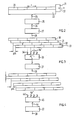
- Fig. 1 refers to a sample of a steel sheet which has two artificial defects in the form of grooves of different widths.
- a signal 9 is obtained as shown at the top of FIG. 1, the two grooves corresponding to the slots 1 and 2. If these are cracks originating for example from an incorrect welding of a steel sheet, the width of the slots is always small compared to the dimensions of a photodetector. It is therefore impossible to establish with such a photodetector a measurement signal which is a faithful image of the cracks.
- fig. 1 shows four bars rettes 3, 4, 5 and 6 of photodetectors such as 7 or 8. It is assumed that the photodetectors are contiguous and that they are arranged at constant p within each strip. The four bars are mutually offset by a distance p / 4 and they are supposed to read the same line of the image simultaneously.
- Photosensitive bars such as those of the CCD (charge coupled device) type are delivered with electronic preprocessing and digital conversion, so that the signals S3 to S6 symbolize the succession of digital values provided by the bars 3 to 6 respectively.
- the signal 9 at the head of FIG. 1 With the position of the various photodetectors of the bars 3 to 6, it is easy to reconstruct the signals S3 to S6.
- the signal S3 begins with two "zero" levels corresponding to the first two photodetectors of this strip, which are not affected by one of the grooves 1 and 2.
- a non-zero value 12 is observed corresponding to the photodetector 8, which covers the entire groove 1.
- the next two detectors again display the value zero and so on.
- the amplitude 12 of a non-zero value is proportional to the integration of the part of the slot such as 1 affected by the detector.
- the detector 8 of the strip 3 covering the entire niche 1 leads to a higher amplitude 12 than that created by the photodetector, which completely covers the niche 2 of narrower width.
- a detector 7 of the strip 6, which only partially covers the slot 1 leads to an amplitude 13 lower than the amplitude 12.
- the four signals S3 to S6 are interleaved or multiplexed to give the oversampled signal S, which comprises a succession of the four amplitudes of the photodetectors of identical rank in the four bars.
- the amplitude 12 of the signal S3 and the amplitude 13 of the signal S6 are marked on the oversampled signal S at their own places.
- the signal S is then subjected to a deconvolution in an autoregressive filter, which performs the reverse filtering to that corresponding to the integration of the signal on the surface of the photodetectors.
- This deconvoluted signal D constitutes an image fairly faithful to the signal at the head of this figure, because this filter is adapted to the particular form of the filtering function during the integration of the signal by the photodetectors (gate function).
- a first embodiment which is shown in FIG. 2, makes use of a single CCD bar 20, which is mechanically coupled to an offset device 21.
- This device comprises a stepping motor, which, after each sampling, moves the bar 20 in the direction of the line (symbolized by an arrow 22) from a distance of p / 4.
- the bar successively takes the positions which correspond to the bars 3, 4, 5, 6 in FIG. 1.
- the bar returns to the original position and a new cycle of four samplings begins after advancing the sheet by one step perpendicular to arrow 22.
- This succession of values is finally applied applie a autoregressive filter 27, whose transfer function is the opposite of that inherent in the spatial smoothing of the photodetectors of the strip.
- the filter is for example of the loop shift register type.
- the pectral aliasing practically no longer distorts the signal S, since the aliasing axis is four times more distant in frequency than in the case of a non-oversampled signal.
- a signal D (see fig. 1) is therefore obtained at the output 28 of this filter, which fairly faithfully represents the shape of the physical signal 9 at the head of FIG. 1.
- fig. 4 shows another variant, which differs from that according to FIG. 3 by a certain distance d between the four bars 40, 41, 42, 43 perpendicular to the offset direction.
- the four bars therefore "read” different lines of the image to be analyzed.
- the oversampling must therefore take into account the scrolling of the image perpendicular to the direction of line.
- each bar is associated with its preprocessing electronics and provides on a single output such as 44 ′ for the bar 40 and 44 ′ ′ for the bar 41 the succession of the values of the line analyzed by the respective bar at a given time. .
Landscapes
- Engineering & Computer Science (AREA)
- Multimedia (AREA)
- Signal Processing (AREA)
- Image Analysis (AREA)
- Analysing Materials By The Use Of Radiation (AREA)
- Image Processing (AREA)
- Facsimile Scanning Arrangements (AREA)
- Investigating Materials By The Use Of Optical Means Adapted For Particular Applications (AREA)
- Photometry And Measurement Of Optical Pulse Characteristics (AREA)
- Image Input (AREA)
- Investigating Or Analysing Materials By Optical Means (AREA)
- Transforming Light Signals Into Electric Signals (AREA)
Abstract
Description
- L'invention se réfère à un procédé de traitement de signaux électriques provenant de l'analyse d'une ligne d'une image issue de détecteurs linéaires tels qu'une barrette de photodétecteurs jointifs qui réalisent un échantillonnage du signal à pas constant. L'invention se réfère également à des dispositifs pour la mise en oeuvre de ce procédé.
- Les barrettes de photodétecteurs, par exemple des photodiodes ou des cellules CCD (charge coupled device), sont utilisées pour analyser une image ligne après ligne, l'image défilant devant la barrette. Une telle image peut, par exemple, provenir d'un appareil de contrôle non destructif par rayons X, des bagages dans les aéroports.
- Les détecteurs intègrent à chaque instant l'énergie lumineuse frappant la surface photosensible du détecteur. Le signal électrique de sortie du détecteur est échantillonné une fois par ligne et il est multiplexé avec les signaux de sortie des autres détecteurs pour constituer le signal d'une ligne de l'image. Le plus souvent, le signal sortant des détecteurs est quantifié pour permettre un traitement ultérieur en numérique.
- A cause de l'intégration du signal lumineux sur la surface photosensible du détecteur, le signal électrique est lissé par rapport au signal lumineux correspondant. L'échantillonnage pose en outre des problèmes de repliement spectral lors que le signal lumineux d'entrée est à large bande. Le lissage correspond à la convolution du signal par une porte centrée sur l'origine; le spectre du signal est multiplié par la fonction de transfert de ce filtre, qui est un sinus cardinal.
- Si le signal lumineux est à large bande, la fonction de transfert du filtre limite l'étendue spectrale du signal lissé. L'effet du filtre de lissage est de privilégier les basses fréquences. On observe donc deux phénomènes qui dégradent l'information dans la bande utile du signal: D'une part, le signal a subi un filtrage basse fréquence et d'autre part, les parties repliées du spectre perturbent les basses fréquences.
- Une diminution éventuelle de la taille de la surface photosensible des photodétecteurs augmenterait certes la résolution, mais ne changerait rien au problème du repliement du spectre. On pourrait penser à faire passer le signal électrique multiplexé dans un filtre dont la fonction de transfert serait l'inverse de celle correspondant à l'intégration de l'information sur la surface photosensible du détecteur. Mais cette correction du spectre n'éliminerait pas les contributions du signal dues au repliement des hautes fréquences.
- L'invention a donc pour but de concevoir un meilleur procédé de traitement de signaux électriques provenant de l'analyse d'une ligne d'une image par au moins une barrette de photodétecteurs jointifs qui réalisent un échantillonnage du signal à pas constant. Ce but est atteint sur le plan du procédé par le fait qu'on effectue k analyses de la même ligne avec des décalages latéraux respectifs de 1/k du pas des photodétecteurs, qu'on génère un signal suréchantillonné en multiplexant les k échantillons et qu'on soumet le signal suréchantillonné à un filtrage temporel inverse au filtrage inhérent au lissage spatial des photodétecteurs.
- En ce qui concerne des dispositifs pour la mise en oeuvre de ce procédé, référence est faite aux revendications correspondantes.
- L'invention sera décrite ci-après plus en détail à l'aide de quelques exemples de mise en oeuvre et des dessins annexés.
- Fig. 1 représente très schématiquement le principe du procédé selon l'invention.
- Fig. 2 est un schéma bloc d'un premier exemple de mise en oeuvre de ce procédé impliquant une barrette unique.
- Fig. 3 est une variante à la fig. 2 impliquant quatre barrettes jointives.
- Fig. 4 est une autre variante impliquant quatre barrettes non jointives.
- La fig. 1 fait référence à un échantillon d'une tôle d'acier qui comporte deux défauts artificiels sous forme de rainures de largeurs différentes. Lorsqu'on balaye cette tôle perpendiculairement aux rainures avec une tête de mesure idéale, on obtient un signal 9 tel que représenté en haut de la fig. 1, les deux rainures correspondant aux créneaux 1 et 2. S'il s'agit de fissures provenant par exemple d'une soudure incorrecte d'une tôle d'acier, la largeur des créneaux est toujours faible par rapport aux dimensions d'un photodétecteur. Il est donc impossible d'établir avec un tel photodétecteur un signal de mesure qui soit une image fidèle des fissures.
- En dessous de ce signal idéal, la fig. 1 montre quatre bar rettes 3, 4, 5 et 6 de photodétecteurs tels que 7 ou 8. On suppose que les photodétecteurs sont jointifs et qu'ils sont disposés au pas p constant au sein de chaque barrette. Les quatre barrettes sont décalées mutuellement d'une distance p/4 et elles sont supposées lire simultanément la même ligne de l'image.
- La fig. 1 montre en outre quatre signaux enregistrés par l'ensemble des photodétecteurs d'une barrette, à savoir un signal S₃ concernant la barrette 3, un signal S₄ concernant la barrette 4, et ainsi de suite pour les barrettes 5 et 6.
- Les barrettes photosensibles telles que celles du type CCD (charge coupled device) sont livrées avec une électronique de prétraitement et de conversion en numérique, de sorte que les signaux S₃ à S₆ symbolisent la succession des valeurs numériques fournies par les barrettes 3 à 6 respectivement. En comparant le signal 9 en tête de la fig. 1 avec la position des différents photodétecteurs des barrettes 3 à 6, on peut facilement reconstituer les signaux S₃ à S₆. Ainsi, le signal S₃ commence avec deux niveaux "zéro" correspondant aux deux premiers photodétecteurs de cette barrette, qui ne sont pas affectés par l'une des rainures 1 et 2. Puis, on observe une valeur 12 non nulle correspondant au photodétecteur 8, qui recouvre la totalité de la rainure 1. Les deux détecteurs suivants affichent de nouveau la valeur zéro et ainsi de suite.
- L'amplitude 12 d'une valeur non nulle est proportionnelle à l'intégration de la partie du créneau tel que 1 affectée par le détecteur. Ainsi, le détecteur 8 de la barrette 3 recouvrant la totalité du créneau 1 conduit à une amplitude 12 plus élevée que celle créée par le photodétecteur, qui recouvre totalement le créneau 2 de largeur plus réduite. De même, un détecteur 7 de la barrette 6, qui ne recouvre que partiellement le créneau 1, conduit à une amplitude 13 plus faible que l'amplitude 12.
- L'analyse du signal optique par une seule barrette de photodétecteur donnerait donc l'un des signaux S₃ à S₆, qui sont loin d'être significatifs pour le signal 9 en tête de la figure. Cela a deux causes principales:
- a) un photodétecteur intègre le signal sur sa surface élémentaire, ce qui entraîne une perte des parties haute fréquence du signal optique, cet effet pouvant être appelé "lissage spatial".
- b) Le signal idéal est échantillonné au pas p. N'ayant accès au signal qu'une fois échantillonné, on observe un repliement spectral lorsque le signal idéal est à large bande. Une diminution de la taille des photodétecteurs certes augmenterait la résolution, mais ne changerait rien au problème de repliement spectral. D'autre part, un filtrage inverse à l'effet de lissage spatial ne permet pas d'éliminer la perturbation des basses fréquences par les hautes fréquences suite au repliement spectral.
- Conformément à l'invention, les quatre signaux S₃ à S₆ sont entrelaçés ou multiplexés pour donner le signal suréchantillonné S, qui comporte une succession des quatre amplitudes des photodétecteurs de rang identique dans les quatre barrettes. Ainsi, l'amplitude 12 du signal S₃ et l'amplitude 13 du signal S₆ sont marquées sur le signal suréchantillonné S aux endroits qui leur sont propres.
- Le signal S est alors soumis à une déconvolution dans un filtre autoregressif, qui réalise le filtrage inverse à celui correspondant à l'intégration du signal sur la surface des photodétecteurs. Ce signal déconvolué D constitue une image assez fidèle du signal figurant en tête de cette figure, car ce filtre est adapté à la forme particulière de la fonction de filtrage lors de l'intégration du signal par les photodétecteurs (fonction porte).
- Le procédé tel qu'il a été expliqué ci-dessus à l'aide de la fig. 1 peut être mis en oeuvre de plusieurs façons. Une première réalisation, qui est représentée sur la fig. 2, fait usage d'une seule barrette CCD 20, qui est mécaniquement couplée à un dispositif de décalage 21. Ce dispositif comporte un moteur pas à pas, qui, après chaque échantillonnage, déplace la barrette 20 en direction de la ligne (symbolisée par une flèche 22) d'une distance de p/4. Ainsi, la barrette prend successivement les positions qui correspondent aux barrettes 3, 4, 5, 6 sur la fig. 1. Puis, la barrette revient vers la position d'origine et un nouveau cycle de quatre échantillonnages commence après l'avance de la tôle d'un pas perpendiculairement à la flèche 22.
- Une barrette de photodétecteur du type CCD du commerce est normalement livrée en association avec une électronique 23 de prétraitement et de conversion en numérique, qui fournit sur une sortie 24 en succession les valeurs correspondant aux différents détecteurs de la barrette. Chaque valeur est par exemple codée sur huit bits, qui sont disponibles en parallèle. Ces valeurs sont appliquées à une mémoire dite de suréchantillonnage 25, dont la capacité correspond au nombre de valeurs provenant de quatre cycles d'échantillonnage de la barrette. A la sortie 26 de cette mémoire, ces valeurs sont entrelaçées de sorte qu'on y dispose d'une succession des quatre échantillons provenant d'un même détecteur et puis les valeurs correspondant aux détecteurs suivants et ainsi de suite. A la sortie 26 on retrouve donc l'équivalent du signal S de la fig. 1. Cette succession de valeurs est enfin appli quée à un filtre autoregressif 27, dont la fonction de transfert est l'inverse de celle inhérente au lissage spatial des photodétecteurs de la barrette. Le filtre est par exemple du type registre à décalage bouclé. Le repliement pectral ne fausse pratiquement plus le signal S, car l'axe de repliement est quatre fois plus éloigné en fréquence que dans le cas d'un signal non suréchantillonné. On obtient donc à la sortie 28 de ce filtre un signal D (voir fig. 1), qui représente assez fidèlement la forme du signal physique 9 à la tête de la fig. 1.
- Si, pour des raisons de rapidité et de stabilité mécanique du dispositif, un décalage pas à pas d'une barrette telle que 20 n'est pas faisable, on utilise quatre barrettes 30, 31, 32, 33, qui sont montées de sorte que ces photodétecteurs reçoivent simultanément la lumière provenant de la même ligne à analyser. Chaque barrette est munie de sa propre électronique de prétraitement telle que 23 (fig. 2) et fournit sur une sortie 34′ (pour la barrette 30) ou 34′′ (pour la barrette 31) et ainsi de suite la succession des valeurs numériques correspondant aux différents détecteurs à un multiplexeur 35, qui a la même fonction que la mémoire de suréchantillonnage 25 de la fig. 2, excepté la mémorisation, et il fournit par sa sortie 36 la suite suréchantillonnée conformément au signal S de la fig. 1. Le filtre autoregressif 27 est le même que précédemment.
- Enfin, la fig. 4 montre une autre variante, qui se distingue de celle conformément à la fig. 3 par une certaine distance d entre les quatre barrettes 40, 41, 42, 43 perpendiculairement à la direction de décalage. A un instant donné, les quatre barrettes "lisent" donc des lignes différentes de l'image à analyser. Le suréchantillonnage doit donc tenir compte du défilement de l'image perpendiculairement à la direction de ligne. Comme précédemment, chaque barrette est associée à son électronique de prétraitement et fournit sur une sortie unique telle que 44′ pour la barrette 40 et 44′′ pour la barrette 41 ls succession des valeurs de la ligne analysée par la barrette respective à un instant donné. C'est une mémoire de synchronisation et de suréchantillonnage 45 qui réarrange les valeurs provenant des différentes barrettes et appartenant à la même ligne, en fonction de la vitesse de défilement perpendiculairement à la direction ce ligne. Cette mémoire doit donc avoir une capacité plus grande que la mémoire 25 de la fig. 1, car elle doit pouvoir stocker une partie de l'image correspondant à la surface couverte par les quatre barrettes et ses interspaces d. A la sortie 46 de cette mémoire, on retrouve alors les mêmes valeurs qu'à la sortie 36 et 26 des figures précédentes, qui sont alors soumises à un filtrage dans un filtre 27 comme précédemment.
- Bien entendu, l'invention n'est pas limitée aux exemples de réalisation décrites ci-dessus. On peut en particulier choisir un taux de suréchantillonnage k autre que quatre. En plus, on peut, outre l'analyse des fissures dans des tôles d'acier à l'aide des rayons X, procéder à l'analyse d'un cliché photographique ou au contrôle non destructif des matériaux par un rayonnement convenable tel que visible, infrarouge ou ultra-violet. Le procédé selon l'invention permet d'améliorer les deux facteurs limitatifs liés à la nature des barrettes de photodétecteurs; à savoir le lissage et le repliement spectral. Grâce au suréchantillonnage on diminue l'effet de repliement du spectre. On peut alors déconvoluer le signal sur une plus grande étendue spectrale. Certes, on obtient toujours une version filtrée passe-bas du signal idéal, mais on dispose d'informations correctes sur un domaine fréquentiel plus large et on a diminué l'effet de lissage des photodétecteurs.
Claims (5)
Applications Claiming Priority (2)
| Application Number | Priority Date | Filing Date | Title |
|---|---|---|---|
| LU87259 | 1988-06-27 | ||
| LU87259A LU87259A1 (fr) | 1988-06-27 | 1988-06-27 | Procede et dispositif de traitement de signaux electriques provenant de l'analyse d'une ligne d'une image |
Publications (2)
| Publication Number | Publication Date |
|---|---|
| EP0348792A1 true EP0348792A1 (fr) | 1990-01-03 |
| EP0348792B1 EP0348792B1 (fr) | 1994-04-20 |
Family
ID=19731066
Family Applications (1)
| Application Number | Title | Priority Date | Filing Date |
|---|---|---|---|
| EP89111156A Expired - Lifetime EP0348792B1 (fr) | 1988-06-27 | 1989-06-20 | Procédé et dispositif de traitement de signaux électriques provenant de l'analyse d'une ligne d'une image |
Country Status (9)
| Country | Link |
|---|---|
| US (1) | US5023921A (fr) |
| EP (1) | EP0348792B1 (fr) |
| JP (1) | JPH02161805A (fr) |
| DE (1) | DE68914727T2 (fr) |
| DK (1) | DK276889A (fr) |
| ES (1) | ES2051930T3 (fr) |
| IE (1) | IE62710B1 (fr) |
| LU (1) | LU87259A1 (fr) |
| PT (1) | PT90978B (fr) |
Cited By (1)
| Publication number | Priority date | Publication date | Assignee | Title |
|---|---|---|---|---|
| EP0494332A1 (fr) * | 1990-01-12 | 1992-07-15 | Fuji Photo Film Co., Ltd. | Appareil de lecture d'images de radiation |
Families Citing this family (11)
| Publication number | Priority date | Publication date | Assignee | Title |
|---|---|---|---|---|
| US5948533A (en) * | 1990-02-09 | 1999-09-07 | Ormet Corporation | Vertically interconnected electronic assemblies and compositions useful therefor |
| US5251037A (en) * | 1992-02-18 | 1993-10-05 | Hughes Training, Inc. | Method and apparatus for generating high resolution CCD camera images |
| US5287619A (en) * | 1992-03-09 | 1994-02-22 | Rogers Corporation | Method of manufacture multichip module substrate |
| US5440805A (en) * | 1992-03-09 | 1995-08-15 | Rogers Corporation | Method of manufacturing a multilayer circuit |
| US5379065A (en) * | 1992-06-22 | 1995-01-03 | The United States Of America As Represented By The Administrator Of The National Aeronautics And Space Administration | Programmable hyperspectral image mapper with on-array processing |
| US5315411A (en) * | 1993-01-04 | 1994-05-24 | Eastman Kodak Company | Dithering mechanism for a high resolution imaging system |
| US6075876A (en) * | 1997-05-07 | 2000-06-13 | Draganoff; Georgi Hristoff | Sliding yardsticks fingerprint enrollment and verification system and method |
| WO2003032627A1 (fr) * | 2001-09-11 | 2003-04-17 | Deltapix Aps | Procede et dispositif permettant de produire une image haute resolution |
| TWI227447B (en) * | 2001-10-26 | 2005-02-01 | Symbol Technologies Inc | Semiconductor device adapted for imaging bar code symbols |
| US7807951B1 (en) | 2004-03-01 | 2010-10-05 | Raytheon Company | Imaging sensor system with staggered arrangement of imaging detector subelements, and method for locating a position of a feature in a scene |
| US7586075B1 (en) | 2004-03-01 | 2009-09-08 | Raytheon Company | Method for analyzing output data of array subelements of an imaging segmented array |
Citations (4)
| Publication number | Priority date | Publication date | Assignee | Title |
|---|---|---|---|---|
| US3697760A (en) * | 1971-08-17 | 1972-10-10 | Comp Generale Electricite | Optical-electrical movement detector utilizing staggered rows of photodetectors and logic for determining the location of a luminous spot |
| FR2385274A1 (fr) * | 1977-03-23 | 1978-10-20 | Cit Alcatel | Dispositif de balayage de document |
| EP0070620A2 (fr) * | 1981-07-20 | 1983-01-26 | Xerox Corporation | Dispositif de formation d'image à haute densité |
| EP0213539A2 (fr) * | 1985-08-20 | 1987-03-11 | Dainippon Screen Mfg. Co., Ltd. | Appareil d'analyse d'images |
Family Cites Families (8)
| Publication number | Priority date | Publication date | Assignee | Title |
|---|---|---|---|---|
| US4147928A (en) * | 1977-05-02 | 1979-04-03 | Xerox Corporation | Scanning array configuration |
| US4092632A (en) * | 1977-05-02 | 1978-05-30 | Xerox Corporation | Crossover arrangement for multiple scanning arrays |
| JPS5741070A (en) * | 1980-08-25 | 1982-03-06 | Canon Inc | Picture reader |
| JPS5769476A (en) * | 1980-10-16 | 1982-04-28 | Fuji Xerox Co Ltd | Reader control system |
| US4910401A (en) * | 1982-01-20 | 1990-03-20 | The Boeing Company | LWIR sensor system with improved clutter rejection |
| US4765564A (en) * | 1985-04-02 | 1988-08-23 | The United States Of America As Represented By The Secretary Of The Interior | Solid state apparatus for imaging with improved resolution |
| JPS61277254A (ja) * | 1985-05-31 | 1986-12-08 | Dainippon Screen Mfg Co Ltd | 画像読取装置 |
| US4913539A (en) * | 1988-04-04 | 1990-04-03 | New York Institute Of Technology | Apparatus and method for lip-synching animation |
-
1988
- 1988-06-27 LU LU87259A patent/LU87259A1/fr unknown
-
1989
- 1989-05-18 US US07/353,435 patent/US5023921A/en not_active Expired - Fee Related
- 1989-06-06 DK DK276889A patent/DK276889A/da not_active Application Discontinuation
- 1989-06-20 ES ES89111156T patent/ES2051930T3/es not_active Expired - Lifetime
- 1989-06-20 EP EP89111156A patent/EP0348792B1/fr not_active Expired - Lifetime
- 1989-06-20 DE DE68914727T patent/DE68914727T2/de not_active Expired - Fee Related
- 1989-06-22 JP JP1158452A patent/JPH02161805A/ja active Pending
- 1989-06-26 PT PT90978A patent/PT90978B/pt not_active IP Right Cessation
- 1989-06-27 IE IE209089A patent/IE62710B1/en not_active IP Right Cessation
Patent Citations (4)
| Publication number | Priority date | Publication date | Assignee | Title |
|---|---|---|---|---|
| US3697760A (en) * | 1971-08-17 | 1972-10-10 | Comp Generale Electricite | Optical-electrical movement detector utilizing staggered rows of photodetectors and logic for determining the location of a luminous spot |
| FR2385274A1 (fr) * | 1977-03-23 | 1978-10-20 | Cit Alcatel | Dispositif de balayage de document |
| EP0070620A2 (fr) * | 1981-07-20 | 1983-01-26 | Xerox Corporation | Dispositif de formation d'image à haute densité |
| EP0213539A2 (fr) * | 1985-08-20 | 1987-03-11 | Dainippon Screen Mfg. Co., Ltd. | Appareil d'analyse d'images |
Non-Patent Citations (1)
| Title |
|---|
| PATENT ABSTRACTS OF JAPAN, vol. 6, no. 77 (E-106)[955], 14 mai 1982, page 52 E 106; & JP-A-57 14 250 (CANON K.K.) 25-01-1982 * |
Cited By (1)
| Publication number | Priority date | Publication date | Assignee | Title |
|---|---|---|---|---|
| EP0494332A1 (fr) * | 1990-01-12 | 1992-07-15 | Fuji Photo Film Co., Ltd. | Appareil de lecture d'images de radiation |
Also Published As
| Publication number | Publication date |
|---|---|
| US5023921A (en) | 1991-06-11 |
| DK276889D0 (da) | 1989-06-06 |
| DK276889A (da) | 1989-12-28 |
| IE892090L (en) | 1989-12-27 |
| LU87259A1 (fr) | 1990-02-28 |
| PT90978A (pt) | 1989-12-29 |
| EP0348792B1 (fr) | 1994-04-20 |
| ES2051930T3 (es) | 1994-07-01 |
| DE68914727T2 (de) | 1994-08-04 |
| JPH02161805A (ja) | 1990-06-21 |
| PT90978B (pt) | 1994-06-30 |
| DE68914727D1 (de) | 1994-05-26 |
| IE62710B1 (en) | 1995-02-22 |
Similar Documents
| Publication | Publication Date | Title |
|---|---|---|
| EP0348792B1 (fr) | Procédé et dispositif de traitement de signaux électriques provenant de l'analyse d'une ligne d'une image | |
| EP0698994A1 (fr) | Assemblage d'un détecteur pour balayeur optique d'image fournissant une échelle de gris et de couleur | |
| US9137470B2 (en) | Digital image processing readout integrated circuit (ROIC) having multiple sampling circuits | |
| EP1080431A1 (fr) | Systeme d'acquisition de donnees comprenant un circuit de conversion d'un signal d'entree analogique haute frequence en une pluralite de signaux numeriques | |
| US20140048683A1 (en) | Readout integrated circuit for dynamic imaging | |
| EP0762145B1 (fr) | Système de traitement d'impulsions provenant de l'interaction d'une particule gamma avec un détecteur de rayonnement CdTe | |
| FR2532504A1 (fr) | Dispositif pour ameliorer le rapport signal-bruit du canal de couleur dans un recepteur de television numerique | |
| US4222077A (en) | Analog-digital conversion method, and a picture reproduction method using the same | |
| WO1992000549A1 (fr) | Procede et dispositif de detection analogique multicanal | |
| EP0983684B1 (fr) | Perfectionnement a l'acquisition d'image par balayage pousse-balai | |
| FR2491274A1 (fr) | Circuit de production d'impulsions periodiques | |
| JPH0682376A (ja) | 表面検査装置 | |
| EP0393763A1 (fr) | Procédé de correction des dispersions des décalages présentés par les détecteurs photoélectriques et dispositif de correction utilisant un tel procédé | |
| Pernechele et al. | Spectral resolution improvement technique for a spectrograph mounting a discrete array detector | |
| EP2782044B1 (fr) | Procédé de lecture d'un code-barres | |
| JP4726065B2 (ja) | エッジ検出方法およびエッジ検出装置 | |
| CN117805070B (zh) | 基于面阵ccd传感器自参考的反射率测量的装置和方法 | |
| Liu et al. | Analysis of oversampling for noise reduction of UV image | |
| FR2737376A1 (fr) | Procede et dispositif pour l'acquisition d'une image par echantillonnage par une barrette ou matrice de detecteurs optiques elementaires a transfert de charge | |
| EP2395361B1 (fr) | Procédé de traitement de signaux RF/hyperfréquence analogiques reçus, de type très large bande, et récepteur mettant en oeuvre un tel procédé | |
| FR2548380A1 (fr) | Procede et dispositif de mesure de temperature et de resistivite d'un element metallique | |
| FR2702325A1 (fr) | Procédé et dispositif de formation d'une image échantillonnée. | |
| JP3534920B2 (ja) | 画像読取装置 | |
| EP2103916B1 (fr) | Spectromètre à transformation de Fourier. | |
| Hawkins et al. | Detailed characterization of advanced technology focal plane arrays |
Legal Events
| Date | Code | Title | Description |
|---|---|---|---|
| PUAI | Public reference made under article 153(3) epc to a published international application that has entered the european phase |
Free format text: ORIGINAL CODE: 0009012 |
|
| AK | Designated contracting states |
Kind code of ref document: A1 Designated state(s): BE DE ES FR GB GR IT LU NL |
|
| 17P | Request for examination filed |
Effective date: 19900627 |
|
| 17Q | First examination report despatched |
Effective date: 19921202 |
|
| GRAA | (expected) grant |
Free format text: ORIGINAL CODE: 0009210 |
|
| AK | Designated contracting states |
Kind code of ref document: B1 Designated state(s): BE DE ES FR GB GR IT LU NL |
|
| REF | Corresponds to: |
Ref document number: 68914727 Country of ref document: DE Date of ref document: 19940526 |
|
| ITF | It: translation for a ep patent filed | ||
| REG | Reference to a national code |
Ref country code: ES Ref legal event code: FG2A Ref document number: 2051930 Country of ref document: ES Kind code of ref document: T3 |
|
| GBT | Gb: translation of ep patent filed (gb section 77(6)(a)/1977) |
Effective date: 19940609 |
|
| EPTA | Lu: last paid annual fee | ||
| REG | Reference to a national code |
Ref country code: GR Ref legal event code: FG4A Free format text: 3012469 |
|
| PLBE | No opposition filed within time limit |
Free format text: ORIGINAL CODE: 0009261 |
|
| STAA | Information on the status of an ep patent application or granted ep patent |
Free format text: STATUS: NO OPPOSITION FILED WITHIN TIME LIMIT |
|
| 26N | No opposition filed | ||
| PGFP | Annual fee paid to national office [announced via postgrant information from national office to epo] |
Ref country code: ES Payment date: 19950427 Year of fee payment: 7 |
|
| PGFP | Annual fee paid to national office [announced via postgrant information from national office to epo] |
Ref country code: GB Payment date: 19950502 Year of fee payment: 7 |
|
| PGFP | Annual fee paid to national office [announced via postgrant information from national office to epo] |
Ref country code: GR Payment date: 19950531 Year of fee payment: 7 |
|
| PGFP | Annual fee paid to national office [announced via postgrant information from national office to epo] |
Ref country code: DE Payment date: 19950613 Year of fee payment: 7 |
|
| PGFP | Annual fee paid to national office [announced via postgrant information from national office to epo] |
Ref country code: FR Payment date: 19950621 Year of fee payment: 7 |
|
| PGFP | Annual fee paid to national office [announced via postgrant information from national office to epo] |
Ref country code: NL Payment date: 19950629 Year of fee payment: 7 |
|
| PGFP | Annual fee paid to national office [announced via postgrant information from national office to epo] |
Ref country code: LU Payment date: 19950701 Year of fee payment: 7 |
|
| PGFP | Annual fee paid to national office [announced via postgrant information from national office to epo] |
Ref country code: BE Payment date: 19950703 Year of fee payment: 7 |
|
| PG25 | Lapsed in a contracting state [announced via postgrant information from national office to epo] |
Ref country code: LU Free format text: LAPSE BECAUSE OF NON-PAYMENT OF DUE FEES Effective date: 19960620 Ref country code: GB Effective date: 19960620 |
|
| PG25 | Lapsed in a contracting state [announced via postgrant information from national office to epo] |
Ref country code: ES Free format text: LAPSE BECAUSE OF EXPIRATION OF PROTECTION Effective date: 19960621 |
|
| PG25 | Lapsed in a contracting state [announced via postgrant information from national office to epo] |
Ref country code: BE Effective date: 19960630 |
|
| BERE | Be: lapsed |
Owner name: COMMUNAUTE EUROPEENNE DU CHARBON ET DE L'ACIER CE Effective date: 19960630 |
|
| PG25 | Lapsed in a contracting state [announced via postgrant information from national office to epo] |
Ref country code: GR Free format text: THE PATENT HAS BEEN ANNULLED BY A DECISION OF A NATIONAL AUTHORITY Effective date: 19961231 |
|
| PG25 | Lapsed in a contracting state [announced via postgrant information from national office to epo] |
Ref country code: NL Effective date: 19970101 |
|
| REG | Reference to a national code |
Ref country code: GR Ref legal event code: MM2A Free format text: 3012469 |
|
| GBPC | Gb: european patent ceased through non-payment of renewal fee |
Effective date: 19960620 |
|
| PG25 | Lapsed in a contracting state [announced via postgrant information from national office to epo] |
Ref country code: FR Effective date: 19970228 |
|
| PG25 | Lapsed in a contracting state [announced via postgrant information from national office to epo] |
Ref country code: DE Effective date: 19970301 |
|
| NLV4 | Nl: lapsed or anulled due to non-payment of the annual fee |
Effective date: 19970101 |
|
| REG | Reference to a national code |
Ref country code: FR Ref legal event code: ST |
|
| REG | Reference to a national code |
Ref country code: ES Ref legal event code: FD2A Effective date: 19991007 |
|
| PG25 | Lapsed in a contracting state [announced via postgrant information from national office to epo] |
Ref country code: IT Free format text: LAPSE BECAUSE OF NON-PAYMENT OF DUE FEES;WARNING: LAPSES OF ITALIAN PATENTS WITH EFFECTIVE DATE BEFORE 2007 MAY HAVE OCCURRED AT ANY TIME BEFORE 2007. THE CORRECT EFFECTIVE DATE MAY BE DIFFERENT FROM THE ONE RECORDED. Effective date: 20050620 |