EP0349360B1 - Verfahren zur magnetischen Charakterisierung der Registrierungsschicht eines magnetischen Informationsträgers - Google Patents
Verfahren zur magnetischen Charakterisierung der Registrierungsschicht eines magnetischen Informationsträgers Download PDFInfo
- Publication number
- EP0349360B1 EP0349360B1 EP19890401579 EP89401579A EP0349360B1 EP 0349360 B1 EP0349360 B1 EP 0349360B1 EP 19890401579 EP19890401579 EP 19890401579 EP 89401579 A EP89401579 A EP 89401579A EP 0349360 B1 EP0349360 B1 EP 0349360B1
- Authority
- EP
- European Patent Office
- Prior art keywords
- magnetic
- values
- amplitude
- current
- value
- Prior art date
- Legal status (The legal status is an assumption and is not a legal conclusion. Google has not performed a legal analysis and makes no representation as to the accuracy of the status listed.)
- Expired - Lifetime
Links
Images



Classifications
-
- G—PHYSICS
- G01—MEASURING; TESTING
- G01R—MEASURING ELECTRIC VARIABLES; MEASURING MAGNETIC VARIABLES
- G01R33/00—Arrangements or instruments for measuring magnetic variables
- G01R33/12—Measuring magnetic properties of articles or specimens of solids or fluids
- G01R33/1207—Testing individual magnetic storage devices, e.g. records carriers or digital storage elements
Definitions
- the present invention relates to a method for magnetically characterizing the recording layer of a magnetic information carrier and the device implementing this method. It is more particularly applicable to the characterization of magnetic drums of magnetographic printers, or of magnetic disks of disk memories.
- Magnetographic printers are now well known and find a preferred use in information processing systems where printing machines are sought which make it possible to obtain the printing of characters of great readability with extremely high printing speeds ( several thousand or even ten thousand lines per minute).
- Such a magnetographic printing machine (also called non-magnetic impact machine) comprises a magnetic recording medium constituted by a magnetic drum itself formed by a magnetic shunt constituting its central part on which a magnetic recording layer is deposited.
- the machine also includes a set of magnetic recording heads placed next to each other parallel to the axis of rotation of the drum. These magnetic heads make it possible to create magnetized domains, also called magnetic points, on the surface of the recording layer of the drum, which is driven by a uniform rotation. Magnetic zones are thus formed formed of a set of magnetic domains, having a shape corresponding to that of the characters that one seeks to print.
- magnetized domains are then coated, by means of a development device, with particles of a powdery magnetic pigment.
- a powdery magnetic pigment consists for example of magnetic particles coated with a resin. It may melt when heated, and become fixed on the printing paper on which it is applied.
- the magnetic pigment adheres to the sets of magnetic domains defined above, forming a deposit of particles on the surface of the drum.
- These particles are then transferred to a sheet of paper applied against the drum by a transfer roller. Then the particles which remain on the drum are removed by an erasing device.
- the procedure is as follows: at the same time as depositing the magnetic recording layer on the magnetic shunt constituting the central part of the drum, a representative sample of the latter is constituted. It consists of a test piece made of brass on which is deposited a strictly identical magnetic material (constituent material, thickness) to that which constitutes the recording layer of the drum.
- the various magnetic characteristics of this sample are measured, for example by means of a commercial magnetometer or a conventional fluxmeter. We check if these properties comply with defined reference standards upper. If this is the case, the drum is then sent to a chromium plating workshop where it is coated with its protective layer of chromium.
- this method does not make it possible to establish the magnetic characteristics of the magnetic recording medium, in particular, to establish in real time the curve of first magnetization of the magnetic recording medium for each of the tracks.
- the present invention overcomes these drawbacks by providing a method for characterizing the magnetic recording layer of a magnetic printing drum, as soon as the manufacturing operations relating thereto are completed (before chromium plating). This characterization takes place for the entire surface of the recording layer of this drum, and is very rapid. It makes it possible to know the magnetic characteristics of the recording layer over the entire surface thereof and to check whether these characteristics are homogeneous, not only on a determined track of the drum but also on all of the recording tracks of this one.
- This invention makes it possible, if a drum does not have the required magnetic characteristics compared to the reference standards, to return the latter to manufacturing and consequently, to avoid disposing of a certain number of magnetic drums, as it was the case in prior practice. Substantial savings are thus obtained, which makes it possible to appreciably reduce the average cost price of the drums.
- This invention is therefore part of the process of improving quality with regard to the manufacture of the drum.
- FIG. 1 shows the various essential constituent elements of a dynamic magnetometer for implementing the method according to the invention, namely MD, intended for magnetically characterizing the TAMB magnetic drum.
- the MEMO memory is contained in a programmable control unit MICROP, which preferably is a microprocessor, which moreover controls the operations of erasing, writing, and reading of the information, respectively carried out by the transducers TEFL, TEC, TEFL .
- MICROP programmable control unit
- the TAMB drum is a cylindrical drum of circular section, the magnetic recording layer of which is made of an alloy of cobalt, nickel and phosphorus Co-Ni-P about 25 micrometers thick deposited on a sub- 0.8 micrometer thick layer of copper itself deposited on a magnetic shunt made of an iron and silicon alloy Fe-Si 100 mm in diameter.
- Each recording track P of the TAMB drum contains a synchronization index IND making it possible to arbitrarily locate the start of each track P. It is obvious that all the index INDs of the tracks of the TAMB drum are aligned on the same generator thereof. this. They are constituted for example by optical marks inscribed on the surface of this drum.
- the MIND locating means consist for example of photoelectronic transducers delivering an electrical pulse I N (see FIG. 6) as soon as the IDE IND of a given track P passes in front of them.
- the TEFL erasing and reading transducer preferably consists of an inductive head of the type commonly used in magnetic tape unwinders, and manufactured for example by the company "Etablatoriums Vedette” in Saverne, 67000 FRANCE, and sold by BULL under reference 993 609 000-01.
- This TEFL inductive head therefore includes a BOBL winding.
- the BOBL winding delivers an analog signal v A to the reading means ML which transform it into a digital signal S which is sent to the memory MEMO of the microprocessor MICROP.
- the reading means ML are controlled by a reading control signal CL sent by the programmable control unit MICROP according to methods which will be described later.
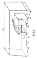
- the TEC write transducer is an inductive type transducer comprising a BOBEC winding. A preferred embodiment of this transducer is shown in FIG. 2.
- This TEC transducer is of the type described in the aforementioned French patent No. 2,522,857. It is of the shoe type, with perpendicular recording, and therefore comprises a POLE writing pole and a PRF flow return pole.
- the thickness e of the POLE writing pole measured in a direction parallel to the direction of travel of the tracks of the drum in front of the transducer is very substantially less than the thickness E of the flux return pole PRF so that once the information has been written by the writing pole POLE, the latter are not disturbed by the PRF flux return pole.
- the section of the POLE writing pole is substantially rectangular and has a width L.
- the order of magnitude of the dimensions e and L is as follows: 0.1 mm for e and 4.8 mm for L.
- the magnetic circuit of the TEC writing transducer is made of a material with high magnetic permeability.
- the BOBEC winding is arranged on the central part PC of the magnetic circuit which connects the POLE writing pole to the PRF flux return pole.
- the TEC writing transducer is preferably embedded in a SURM overmold having a width greater than the width of the TEC transducer and is made of a non-magnetic material such as a thermosetting resin.
- the underside of the SURM overmolding intended to be placed facing the drum TAMB is composed of three adjacent planar faces, namely the faces F1, F2, F3, the face F2 being between the faces F1 and F3, the lines of intersection of F1 and F2, on the one hand, F2 and F3, on the other hand, being parallel.
- the face F1 forms a dihedral angle D1 with the face F2, the latter making a dihedral angle D2 with the face F3.
- the dihedral angle D1 is greater than the dihedral angle D2.
- the microprocessor MICROP sends a writing control current CE in digital form to the writing current generation means MGCE, which transform this digital control current and an analog writing current SC having for example a square shape as shown in Figure 4.
- the period of this writing current SC is equal to T, its amplitude equal to I.
- This current SC is alternately positive and negative alternately and the intensity thereof varies so between - I and + I.
- This write current SC feeds the BOBEC winding of the TEC write transducer.
- the operation of the dynamic magnetometer MD is governed by the method described below, in relation to FIGS. 1, 4, 5, 6.
- the index IND passes in front of the locating means MIND, the latter deliver a pulse I N of rectangular shape.
- the MIND means deliver a succession of pulses I N-2 , I N-1 , I N , I N + 1 , ..., the duration separating each of these pulses being equal the rotation time of one drum revolution.
- This erasure current can be either a direct current, for example of intensity equal to 150 milliamperes, than an alternating current, for example of frequency 7 kHz, and of amplitude 150 milliamperes.
- the erasure of track P of the drum takes place for a complete revolution of the latter, that is to say until the means of locating the index MIND deliver the pulse which follows the pulse.
- I N-2 i.e. the pulse I N-1 .
- the essential result of this erasure is that the magnetic recording layer of the drum is made magnetically neutral (magnetization inside the null layer).
- the MICROP microprocessor receives the pulse I N-1 , then begins the operation of writing information on the track P of the drum.
- the microprocessor MICROP sends a write command signal CE to the means MGCE.
- the latter transform the write command current CE written in digital form into a square current SC (see FIG. 4 and description above).
- the TEC writing transducer then writes on track P a succession of rectangular magnetic domains having substantially the dimension of the section of the POLE writing pole.
- the writing operation is terminated. It should be noted that during this writing operation, the reading means ML are inhibited. As soon as the MICROP microprocessor receives the pulse I N , the read operation begins.
- the microprocessor MICROP then sends a read control signal CL to the reading means ML which can then operate.
- the BOBL winding of the TEFL reading transducer then delivers the signal v A to the reading means ML.
- This signal v A is a periodic signal whose period is equal to T. It has a substantially sinusoidal shape having a series of positive and negative alternations, the amplitude of the positive alternations being successively V1, V2, ..., V n .
- the microprocessor delivers to the means ML a succession of sampling pulses SA n , SA n +1, ..., whose sampling period T E is equal to several times the period T, for example 7 times in a preferred embodiment of the invention.
- the time scale is different for the signals I N , on the one hand, I Dn , S An and V A on the other hand).
- the reading means ML receive one of the sampling pulses SA n , SA n + 1 , ..., they take the value of the positive amplitude of the signal v A at the instant t n where is emitted the pulse SA n and transforms it into a digital signal S1 which is sent to the memory MEMO.
- the digital signal S1 is formed for example by a set of 10 logic bits equal to 0 or 1.
- the drum having a circumference of 314 mm (diameter equal to 100 mm), the length e of a magnetic domain being 0.1 mm, we see that, per revolution, there are 1570 pairs of positive and negative magnetic domains such as A i -A i + 1 , and therefore the signal V A has 1570 periods.
- T E is substantially equal to 7 T, it can be seen that more than 200 values of S1 can be sampled which will be sent to the MEMO memory, for the same rotation of the drum, for the same value of I1.
- the MICROP microprocessor includes a calculation program allowing it to extract from the 200 measurement points, the maximum value S M1 , the minimum value S m1 and the average value of all the values S1 recorded for the same rotation of the drum.
- the sequence of operations SEQ2, takes place in the same order as before, that is to say successively erasing, writing, reading.
- Three signal values S M2 , S a2 , S m2 are thus obtained which correspond to the value of the current I2.
- I p correspond three sets of values, namely a first set S M1 , S M2 , ..., S Mp , a second set S a1 , S a2 , ..., S ap and a third set S m1 , S m2 , ..., S mp .
- the characterization by means of said device of a magnetic drum takes place, as indicated above, as soon as the various stages of manufacture of this same drum are completed and this before and / or after chromium plating thereof .
- the means for generating the writing current MGCE are constituted by a digital analog converter CDAE and by a current generator GCE placed in series.
- the digital analog converter CDAE receives the digital write command signal CE which is a set of 8 logic bits equal to 0 or 1 indicating both the amplitude and the frequency of the square signal SC.
- the microprocessor MICROP corresponds to the output of the digital analog converter CDAE a series of voltage pulses VCE transformed into a series of current pulses by the current generator GCE.
- the latter therefore delivers the square signal SC represented in FIG. 4 which has the amplitude I and the desired frequency.
- the frequency of this current is chosen so that the length e of written information is equal to or greater than 0.1 mm.
- the signal v A from the BOBL winding of the TEML read transducer is sent to the input of the AMP preamplifier, and amplified by the latter in becoming the signal V A which is sent to the input of the FILT filter of the capacitance switching type, for example an MF10 filter from the firm NS (National Semiconductors) and comes out in the form of a substantially sinusoidal frequency read signal strictly equal to the frequency of the write current.
- the role of the filter which is calibrated on the frequency of the writing current is to rid the signal V A of all its harmonics and of all the parasitic signals.
- the signal V A having thus passed through the filter is sent to the input of the data acquisition voltmeter VAD whose essential functional components are shown in FIG. 3b.
- This VAD data acquisition voltmeter is actually an analog peak voltmeter.
- the common terminal (not connected to ground) to the capacitor CAP, to the resistor R and to the switch INT is also connected to the negative input E N of the comparator COMP and to the cathode of the diode DI. Their other common terminal is connected to ground.
- the voltage V A is applied to the positive input E p of the comparator COMP, the output of which is connected to the anode of the diode DI.
- the voltage V C at the terminals of the capacitor CAP changes as indicated in FIG. 6, as will be detailed below.
- the MICROP microprocessor As soon as the index pulse I N is sent to the MICROP microprocessor, the latter sends a discharge signal I Dn to the INT switch which closes.
- the capacitor CAP discharges quickly (with a duration of the order of that of the pulse I Dn , itself less than that of a half-wave of the signal V A ). In FIG. 6, it has been assumed, to simplify the figure and the reasoning, that this discharge takes place during a negative alternation of the signal V A. The voltage V C is therefore zero, at the end of the discharge.
- the INT switch opens.
- the diode DI is conductive (since V A > V C ) the capacitor charges until its voltage across V C is equal to the peak voltage V1 of this alternation.
- V A becomes less than V C
- the diode DI no longer conducts and the capacitor CAP then discharges through the resistor R, very slowly, the discharge period T D equal to the product of R by the capacity of the capacitor CAP being of the order of 100 times the period T.
- the diode DI conducts and the capacitor CAP charges again until, as indicated in FIG.
- V C at the terminals is equal for example to the peak voltage V2 of the second positive half-wave.
- V A becomes less than V2
- the capacitor CAP again discharges through the resistor R (the diode DI no longer conducting) until V A becomes again greater than V C , which is the case for the seventh alternation shown in Figure 6 where V C then becomes equal to the peak voltage V7 thereof.
- the sampling pulse SA n is sent to the CADL converter which then takes the analog value V C (practically equal to V7 in FIG. 6) and transforms it into a digital signal having for example 10 bits D0 to D9 which constitutes the signal S sent to the memory MEMO.
- FIG. 7 and 8 show a preferred embodiment of said dynamic magnetometer.
- the TEC write transducer and its SURM overmold (see FIG. 2), and the TEFL erase and read transducer are mounted on the same mobile transducer arm, namely EQM, which is mobile. in a direction parallel to the generators of the TAMB drum.
- the EQM arm moves in the directions F1 or F2 as shown in Figure 7. It is for example made of the same material which constitutes the overmolding SURM. It is provided with two holes TR1 and TR3 inside which pass two cylindrical rods TIG1 and TIG2 whose axis is parallel to the generatrices of the drum and on which slides the moving assembly to move from a track P, to the tracks neighbors.
- the EQM arm is also provided with a threaded hole TR2 inside which passes an endless screw VIS secured to the drive shaft of a motor M, for example of the stepping type, the pitch of which is equal to the width L of the tracks P of the drum.
- a motor M for example of the stepping type
- the pitch of which is equal to the width L of the tracks P of the drum.
Landscapes
- Physics & Mathematics (AREA)
- Condensed Matter Physics & Semiconductors (AREA)
- General Physics & Mathematics (AREA)
- Recording Or Reproducing By Magnetic Means (AREA)
- Measuring Magnetic Variables (AREA)
- Magnetic Record Carriers (AREA)
- Manufacturing Of Magnetic Record Carriers (AREA)
Claims (4)
- Verfahren zum Erstellen der magnetischen Eigenschaften einer ersten Magnetisierung der Aufzeichnungsschicht eines beweglichen magnetischen Informationsträgers, der mehrere Aufzeichnungsspuren (P) aufweist, die jeweils einen Synchronisationsindex (IND) besitzen, der von Ortungsmitteln (MIND) geortet wird, die bei jeder Vorbeibewegung des Indexes vor ihnen einen Synchronisationsimpuls (IN-2, IN-1, IN,...) ausgeben, wobei in dem Verfahren für jede Spur wenigstens eine die folgenden Operationen umfassende Sequenz ausgeführt wird:1) magnetisches Löschen der Schicht auf der gesamten Fläche der Spur, derart, daß ihr magnetischer Zustand neutralisiert wird,2) anschließend Beschreiben dieser gesamten Fläche mit einer Reihe von magnetischen Bereichen (Ai, Ai+1, Ai+2) mittels eines Magnetfeldes (H), das von einem periodischen Schreibstrom (SC) erzeugt wird,3) anschließend in bestimmten Abtastzeitpunkten (tn, tn+1,...) Lesen einer Spannung (S), die von der Magnetisierung (M) im Inneren eines jeden in diesen Zeitpunkten gelesenen Bereichs abhängt,4) Speichern dieser Spannungen und Berechnen des Mittelwertes (Saj) und Anzeigen derselben mittels einer Anzeigeeinrichtung,dadurch gekennzeichnet, daß es eine Reihe von verschiedenen Sequenzen mit der Anzahl p umfaßt, wobei p eine ganze Zahl ist (Seq1, Seq2, Seqj,..., Seqp), wobei die Operationen 1) bis 4) in jeder Sequenz außerdem die folgenden Besonderheiten aufweisen:1/ die Löschung der Schicht findet ab dem Empfang eines ersten Synchronisationsimpulses (IN-2) statt,2/ beim Empfang eines zweiten Synchronisationsimpulses (IN-1) besitzt der Schreibstrom (SC) eine bestimmte Amplitude (Ij), wobei die Folge der Amplituden (I1, I2, Ij,..., Ip) anwächst, wobei die maximale Amplitude (Ip) derjenige Amplitudenwert (Ij) ist, bei dem die magnetische Schicht gesättigt ist, wobei die minimale Amplitude (I1) der am nächsten bei Null liegende Wert ist, wobei der Strom einer bestimmten Amplitude (Ij) in der Operation 2) der entsprechenden Sequenz (SEQj) ab dem Empfang des zweiten Synchronisationsimpulses zugeführt wird,3/ ab dem Empfang eines dritten Synchronisationsimpulses (IN) wird das Lesen in den genannten Abtastzeitpunkten mit einer bestimmten Abtastperiode (TE) ausgeführt, die größer als die Periode (T) des Schreibstroms ist, wobei die gelesene Spannung (S) in diesen Abtastzeitpunkten von der Magnetisierung (M) im Inneren eines jeden der in diesen Zeitpunkten gelesenen Bereiche abhängt, derart, daß für denselben Stromamplitudenwert (Ij) mehrere Werte der gelesenen Spannung (S) erhalten werden,4/ die Gesamtheit der Werte der gelesenen Spannungen (S) und der entsprechende Stromamplitudenwert (Ij) werden gespeichert und der Mittelwert (Saj) der gelesenen Spannung (S) wenigstens dieser Gesamtheit wird berechnet, wobei die Mittelwertkurve der ersten Magnetisierung, die die Gesamtheit dieser Mittelwerte (Sal, Saj,..., Sap) enthält, als Funktion dieser Stromamplitudenwerte (I1,..., Ip) auf der Anzeigeeinrichtung dargestellt wird, sobald die letzte der Sequenzen (SEQp) beendet ist.
- Verfahren gemäß Anspruch 1, dadurch gekennzeichnet, daß die Wertedifferenz zwischen zwei Stromamplituden, die zwei aufeinanderfolgenden Sequenzen entsprechen, von den Werten der maximalen Stromamplitude (Ip) und von der Anzahl (p) der Sequenzen abhängt.
- Verfahren gemäß einem der Ansprüche 1, 2, dadurch gekennzeichnet, daß außerdem aus der Gesamtheit der Werte der gelesenen Spannungen (S), die jedem der Werte des Schreibstroms (Ij) entsprechen, der Maximalwert (SMj) und der Minimalwert (Smj) berechnet werden, wodurch eine die Gesamtheit der Maximalwerte enthaltende Maximalwertkurve der ersten Magnetisierung und eine die Gesamtheit der Minimalwerte der gelesenen Spannungen enthaltende Minimalwertkurve der ersten Magnetisierung erhalten werden, wobei diese Kurven auf der Anzeigeeinrichtung in Abhängigkeit von den aufeinanderfolgenden Werten der Schreibstromamplitude (I1 bis Ip) dargestellt werden.
- Verfahren gemäß Anspruch 3, dadurch gekennzeichnet, daß die Maximalwertkurve, die Mittelwertkurve und die Minimalwertkurve mittels der Anzeigeeinrichtung mit Maximalwert-, Mittelwert- bzw. Minimalwert-Referenzkurven (CR1, CR2, CR3) eines magnetischen Referenzträgers verglichen werden.
Applications Claiming Priority (2)
| Application Number | Priority Date | Filing Date | Title |
|---|---|---|---|
| FR8808773A FR2633724B1 (fr) | 1988-06-29 | 1988-06-29 | Procede pour caracteriser magnetiquement la couche d'enregistrement d'un support magnetique d'informations et dispositif de mise en oeuvre de ce procede |
| FR8808773 | 1988-06-29 |
Publications (2)
| Publication Number | Publication Date |
|---|---|
| EP0349360A1 EP0349360A1 (de) | 1990-01-03 |
| EP0349360B1 true EP0349360B1 (de) | 1993-05-12 |
Family
ID=9367876
Family Applications (1)
| Application Number | Title | Priority Date | Filing Date |
|---|---|---|---|
| EP19890401579 Expired - Lifetime EP0349360B1 (de) | 1988-06-29 | 1989-06-07 | Verfahren zur magnetischen Charakterisierung der Registrierungsschicht eines magnetischen Informationsträgers |
Country Status (5)
| Country | Link |
|---|---|
| US (1) | US4978916A (de) |
| EP (1) | EP0349360B1 (de) |
| JP (1) | JPH06103423B2 (de) |
| DE (1) | DE68906468T2 (de) |
| FR (1) | FR2633724B1 (de) |
Families Citing this family (2)
| Publication number | Priority date | Publication date | Assignee | Title |
|---|---|---|---|---|
| KR100299376B1 (ko) * | 1998-05-29 | 2002-06-20 | 박종섭 | 다중 도메인을 갖는 수직 배향 모드의 액정 표시 장치 |
| JP3744781B2 (ja) * | 2000-09-13 | 2006-02-15 | 株式会社アイメス | 磁気ヘッドまたは磁気ディスクの試験装置および試験方法 |
Family Cites Families (6)
| Publication number | Priority date | Publication date | Assignee | Title |
|---|---|---|---|---|
| US3686682A (en) * | 1970-08-17 | 1972-08-22 | Burroughs Corp | Method and apparatus for testing magnetic disc files |
| US3781835A (en) * | 1973-02-16 | 1973-12-25 | Memorex Corp | Method of certifying magnetic recording disc |
| SU664134A1 (ru) * | 1977-01-25 | 1979-05-25 | Московский Ордена Трудового Красного Знамени Электротехнический Институт Связи | Устройство дл определени петель гистерезиса движущегос магнитного носител |
| JPS5888675A (ja) * | 1981-11-24 | 1983-05-26 | Hitachi Ltd | 磁気デイスク媒体のテスト方法 |
| FR2522857B1 (fr) * | 1982-03-03 | 1988-01-22 | Cii Honeywell Bull | Dispositif d'ecriture et/ou de lecture d'informations sur un support magnetique, a frottements reduits contre ce support |
| JPS60123783A (ja) * | 1983-12-07 | 1985-07-02 | Matsushita Electric Ind Co Ltd | 磁気記録媒体の品質検査装置 |
-
1988
- 1988-06-29 FR FR8808773A patent/FR2633724B1/fr not_active Expired - Lifetime
-
1989
- 1989-06-07 EP EP19890401579 patent/EP0349360B1/de not_active Expired - Lifetime
- 1989-06-07 DE DE89401579T patent/DE68906468T2/de not_active Expired - Fee Related
- 1989-06-26 US US07/371,532 patent/US4978916A/en not_active Expired - Lifetime
- 1989-06-28 JP JP1166472A patent/JPH06103423B2/ja not_active Expired - Fee Related
Also Published As
| Publication number | Publication date |
|---|---|
| FR2633724A1 (fr) | 1990-01-05 |
| US4978916A (en) | 1990-12-18 |
| FR2633724B1 (fr) | 1990-08-10 |
| EP0349360A1 (de) | 1990-01-03 |
| JPH0264479A (ja) | 1990-03-05 |
| DE68906468D1 (de) | 1993-06-17 |
| DE68906468T2 (de) | 1993-10-21 |
| JPH06103423B2 (ja) | 1994-12-14 |
Similar Documents
| Publication | Publication Date | Title |
|---|---|---|
| EP0089274B1 (de) | Optischer Informationsträger, optische Anordnung zur Spurfolge und optische Anordnung zur Erzeugung eines Fehlersignals zur Scharfeinstellung | |
| EP0369989B1 (de) | Vorgeprägter beweglicher Informationsträger und optische Spurfolgeanordnung dafür | |
| EP0467737B1 (de) | Magnetische Wiedergabevorrichtung mit einem matrixartigen Netzwerk von Leseköpfen | |
| EP0006482B1 (de) | Schaltung zur Erkennung der Maxima und Minima eines elektrischen Signals variabler Amplitude und niedriger Frequenz sowie Verwendung dieser Schaltung, um bei zwei sich zueinander bewegenden Objekten Ausmass und Richtung der Bewegung zu bestimmen | |
| EP0126682A1 (de) | Verfahren und Vorrichtung zur Festlegung der für Datenaufnahme auf eine optische Scheibe aufgebrachten optischen Leistung | |
| FR2517103A1 (fr) | Appareil d'enregistrement et de reproduction d'informations | |
| FR2466073A1 (fr) | Systeme d'organisation et de positionnement de donnees sur une bande magnetique | |
| FR2581784A1 (fr) | Support d'information a pregravure et son dispositif de lecture optique | |
| EP3037898A1 (de) | Elektromechanisches gerät, das einen kapazitiven detektor der winkelposition eines mobilen elementes umfasst, und verfahren zur detektion der winkelposition eines mobilen elementes | |
| FR2558001A1 (fr) | Procede et appareil pour la recherche d'une piste sur un support optique d'information. | |
| EP0467736A1 (de) | Magnetoresistiver Effekt verwendender Lesemagnetkopf | |
| EP0349360B1 (de) | Verfahren zur magnetischen Charakterisierung der Registrierungsschicht eines magnetischen Informationsträgers | |
| FR2567673A1 (fr) | Support d'information inscriptible optiquement selon une piste definie par des motifs de pregravure et dispositif optique de suivi de piste mettant en oeuvre un tel support | |
| FR2786005A1 (fr) | Procede d'ecriture et de lecture d'un support d'informations comprenant un materiau avec une succession de zones presentant respectivement un premier et un deuxieme etats physiques | |
| EP0148077A2 (de) | Verfahren zur Aufzeichnung von Informationen auf einem Aufzeichnungsträger | |
| EP0032324B1 (de) | Verfahren zur Verstärkungsregelung von Schaltungsanordnungen zum Verstärken von Signalen, die von einem Lesekopf abgegeben werden, der mit einem Informations-Aufzeichnungsträger gekoppelt ist, und Vorrichtung zur Ausführung des Verfahrens | |
| EP0061363A1 (de) | Magnetoresistiver Lesewandler für grosse Informationsdichtheit | |
| FR2514913A1 (fr) | Dispositif opto-electronique de lecture d'informations contenues sur un support magnetique | |
| EP0006441A2 (de) | Optische Anordnung für ein Positionsdetektionsapparat mit einem auf sich selbst reflektierten Gitter | |
| EP0434547A1 (de) | Mehrspur-Lesemagnetkopf | |
| FR2470425A1 (fr) | Procede pour mesurer la position d'une tete de lecture-ecriture des informations d'un support par rapport a une position de reference de celui-ci et dispositif pour le mettre en oeuvre | |
| FR2468183A1 (fr) | Transducteur magnetique integre | |
| EP0094852A1 (de) | Opto-elektronisches Verfahren zum Lesen von Informationen von einer magnetischen Platte und Anordnung dafür | |
| FR2468180A1 (fr) | Dispositif de translation d'une aiguille de lecture a adaptation | |
| WO1989009978A1 (fr) | Procede d'impression magnetographique et appareil pour la mise en oeuvre du procede |
Legal Events
| Date | Code | Title | Description |
|---|---|---|---|
| PUAI | Public reference made under article 153(3) epc to a published international application that has entered the european phase |
Free format text: ORIGINAL CODE: 0009012 |
|
| AK | Designated contracting states |
Kind code of ref document: A1 Designated state(s): DE FR GB IT NL |
|
| 17P | Request for examination filed |
Effective date: 19900118 |
|
| 17Q | First examination report despatched |
Effective date: 19920224 |
|
| GRAA | (expected) grant |
Free format text: ORIGINAL CODE: 0009210 |
|
| AK | Designated contracting states |
Kind code of ref document: B1 Designated state(s): DE FR GB IT NL |
|
| ITF | It: translation for a ep patent filed | ||
| REF | Corresponds to: |
Ref document number: 68906468 Country of ref document: DE Date of ref document: 19930617 |
|
| GBT | Gb: translation of ep patent filed (gb section 77(6)(a)/1977) |
Effective date: 19930621 |
|
| RAP4 | Party data changed (patent owner data changed or rights of a patent transferred) |
Owner name: BULL S.A. |
|
| REG | Reference to a national code |
Ref country code: GB Ref legal event code: IF02 |
|
| PGFP | Annual fee paid to national office [announced via postgrant information from national office to epo] |
Ref country code: GB Payment date: 20050527 Year of fee payment: 17 Ref country code: DE Payment date: 20050527 Year of fee payment: 17 |
|
| PG25 | Lapsed in a contracting state [announced via postgrant information from national office to epo] |
Ref country code: GB Free format text: LAPSE BECAUSE OF NON-PAYMENT OF DUE FEES Effective date: 20060607 |
|
| PGFP | Annual fee paid to national office [announced via postgrant information from national office to epo] |
Ref country code: FR Payment date: 20060629 Year of fee payment: 18 |
|
| PGFP | Annual fee paid to national office [announced via postgrant information from national office to epo] |
Ref country code: IT Payment date: 20060630 Year of fee payment: 18 |
|
| PG25 | Lapsed in a contracting state [announced via postgrant information from national office to epo] |
Ref country code: DE Free format text: LAPSE BECAUSE OF NON-PAYMENT OF DUE FEES Effective date: 20070103 |
|
| GBPC | Gb: european patent ceased through non-payment of renewal fee |
Effective date: 20060607 |
|
| PGFP | Annual fee paid to national office [announced via postgrant information from national office to epo] |
Ref country code: NL Payment date: 20070528 Year of fee payment: 19 |
|
| REG | Reference to a national code |
Ref country code: FR Ref legal event code: ST Effective date: 20080229 |
|
| PG25 | Lapsed in a contracting state [announced via postgrant information from national office to epo] |
Ref country code: FR Free format text: LAPSE BECAUSE OF NON-PAYMENT OF DUE FEES Effective date: 20070702 |
|
| NLV4 | Nl: lapsed or anulled due to non-payment of the annual fee |
Effective date: 20090101 |
|
| PG25 | Lapsed in a contracting state [announced via postgrant information from national office to epo] |
Ref country code: NL Free format text: LAPSE BECAUSE OF NON-PAYMENT OF DUE FEES Effective date: 20090101 |
|
| PG25 | Lapsed in a contracting state [announced via postgrant information from national office to epo] |
Ref country code: IT Free format text: LAPSE BECAUSE OF NON-PAYMENT OF DUE FEES Effective date: 20070607 |
|
| PLBE | No opposition filed within time limit |
Free format text: ORIGINAL CODE: 0009261 |
|
| STAA | Information on the status of an ep patent application or granted ep patent |
Free format text: STATUS: NO OPPOSITION FILED WITHIN TIME LIMIT |