EP0349495A2 - CMOS-Spannungsmultiplikator - Google Patents
CMOS-Spannungsmultiplikator Download PDFInfo
- Publication number
- EP0349495A2 EP0349495A2 EP89830269A EP89830269A EP0349495A2 EP 0349495 A2 EP0349495 A2 EP 0349495A2 EP 89830269 A EP89830269 A EP 89830269A EP 89830269 A EP89830269 A EP 89830269A EP 0349495 A2 EP0349495 A2 EP 0349495A2
- Authority
- EP
- European Patent Office
- Prior art keywords
- voltage
- transistor
- cmos
- absolute value
- intermediate node
- Prior art date
- Legal status (The legal status is an assumption and is not a legal conclusion. Google has not performed a legal analysis and makes no representation as to the accuracy of the status listed.)
- Granted
Links
Images
Classifications
-
- G—PHYSICS
- G11—INFORMATION STORAGE
- G11C—STATIC STORES
- G11C16/00—Erasable programmable read-only memories
- G11C16/02—Erasable programmable read-only memories electrically programmable
- G11C16/06—Auxiliary circuits, e.g. for writing into memory
- G11C16/30—Power supply circuits
-
- G—PHYSICS
- G11—INFORMATION STORAGE
- G11C—STATIC STORES
- G11C5/00—Details of stores covered by group G11C11/00
- G11C5/14—Power supply arrangements, e.g. power down, chip selection or deselection, layout of wirings or power grids, or multiple supply levels
- G11C5/145—Applications of charge pumps; Boosted voltage circuits; Clamp circuits therefor
-
- H—ELECTRICITY
- H02—GENERATION; CONVERSION OR DISTRIBUTION OF ELECTRIC POWER
- H02M—APPARATUS FOR CONVERSION BETWEEN AC AND AC, BETWEEN AC AND DC, OR BETWEEN DC AND DC, AND FOR USE WITH MAINS OR SIMILAR POWER SUPPLY SYSTEMS; CONVERSION OF DC OR AC INPUT POWER INTO SURGE OUTPUT POWER; CONTROL OR REGULATION THEREOF
- H02M3/00—Conversion of DC power input into DC power output
- H02M3/02—Conversion of DC power input into DC power output without intermediate conversion into AC
- H02M3/04—Conversion of DC power input into DC power output without intermediate conversion into AC by static converters
- H02M3/06—Conversion of DC power input into DC power output without intermediate conversion into AC by static converters using resistors or capacitors, e.g. potential divider
- H02M3/07—Conversion of DC power input into DC power output without intermediate conversion into AC by static converters using resistors or capacitors, e.g. potential divider using capacitors charged and discharged alternately by semiconductor devices with control electrode, e.g. charge pumps
- H02M3/073—Charge pumps of the Schenkel-type
Definitions
- the present invention relates to a fully integrated, CMOS voltage multiplier particularly useful for EPROM and EEPROM memory devices.
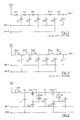
- the voltage multiplier is a well known circuit and a diagram thereof is depicted in Fig. 1.
- Phi 1 and phi 2 are two square-wave signals, substantially in phase opposition between themselves, generated by a suitable oscillator.
- the diodes and the square-wave signals By supposing ideal the diodes and the square-wave signals to have an amplitude equal to the supply voltage Vcc, the asymptotic level approached by the output voltage Vout, in an open circuit situation, is equal to n times Vcc, wherein n is the number of stages of the multiplier circuit.
- Said output resistance Ro may be easily calculated through a simplified analysis of the multiplier circuit.
- Vt Vto + ⁇ ( ⁇
- Vto the threshold voltage when the voltage difference between source and body (Vsb) is equal to zero
- ⁇ F the electrostatic potential of the p-type substrate at equilibrium and ⁇ is an empirically evaluated constant depending on the specific fabrication process used.
- the threshold remains higher than 1.5 V, i.e. much higher than that of bipolar diodes.
- the entirely integrated, CMOS voltage multiplier object of the present invention permits the charge transfer from a stage to a successive stage of the multiplier circuit through a diode equivalent structure, the threshold of which is substantially nil, and therefore favors such a charge transfer also with a relatively low supply voltage, besides naturally favoring the achievement of a high output voltage with a lesser number of stages.
- circuits shown in the figures relates to the case of a voltage multiplier for a positive voltage and, for an easy comparison, the succession of identification numbers of the repeatitive stages of the circuit has been maintained uniform as far as possible in all the figures. Obviously, in case of voltage multipliers for negative voltages, all polarities will be inverted.
- the voltage multiplier circuit of the invention utilizes a diode equivalent structure, the threshold voltage of which is determined by the difference between the threshold voltages of two MOS transistors.
- a difference which may be defined by analogy what discussed above as an equivalent Vt, is nil for similar transistors, and therefore favors charge transfer under a relatively low supply voltage.
- such a diode equivalent structure is substantially represented by an enhancement type CMOS transistor, which in the embodiment shown is a p-channel transistor (T2a, T3a, ...), having a source and a drain functionally connected respectively to a first intermediate node and to a successive second intermediate node (i.e. to the input and output of any one stage of the multiplier circuit) or to the output terminal Vout of the multiplier circuit, not shown in Fig. 3).
- CMOS transistor which in the embodiment shown is a p-channel transistor (T2a, T3a, ...), having a source and a drain functionally connected respectively to a first intermediate node and to a successive second intermediate node (i.e. to the input and output of any one stage of the multiplier circuit) or to the output terminal Vout of the multiplier circuit, not shown in Fig. 3).
- This p-channel transistor is coupled by means of a coupling capacitor (Cc2, Cc3, ...) to the rail of the square-wave switching signal (phi 1 or phi 2) to which the respective output capacitor of the particular stage of the multiplier (C2, C3, ...) is connected.
- a second CMOS transistor (T2b, T3b, ...) of the same type of the charge transfer transistor (T2a, T3a, ...) and having essentially the same threshold voltage of the latter is connected in a diode configuration between the drain and the gate of the charge transfer transistor.
- each multiplying stage of the voltage multiplier circuit of the invention may be described as follows, making reference to one of said stages formed by the charge transfer transistor T2a and by the respective output capacitor C2 and comprised between the two intermediate nodes A and B of the circuit of Fig. 3.
- phase opposition square-wave switching signals phi 1 and phi 2 are not only applied across the capacitors used for transferring the electrical charge: C1, C2, C3, ..., etc., but also to the gate of the transistor T2a through the relative coupling capacitor Cc2.
- the transistor T2a When the two signals phi 1 and phi 2 switch, the transistor T2a must be in a cut-off condition in order to prevent an undue back flow of electrical charge. This is ensured by the fact that the B node voltage and therefore the gate voltage of the transistor T2a rises because the phi 1 signal assumes a high level, commonly equal to the supply voltage Vcc, and consequently the transistor T2a which was OFF at the end of the preceding semicycle, remains in such a condition until the next switching of the two phases phi 1 and phi 2. Simultaneously, in a totally similar manner, the transistor T3a will start conducting and the capacitor C2 will pour charge into the following stage (C3), through a repetition of events described above.
- the voltage multiplier circuit may also employ initial stages of a conventional type being the utility of stages made in accordance with the present invention particularly felt in the final output stages of the circuit. It is therefore possible to make one or more initial stages of the multiplier circuit in accordance with the prior art. In this respect, it may be observed in Fig. 3 that the first "diode" De1 is made by utilizing a diode-connected NMOS transistor, as in a prior art circuit.
- CMOS voltage multiplier capable of transferring charge with a low voltage drop across the charge transfer "diodes" and therefore suitable to operate with a relatively low supply voltage is fully met without recurring to complex modifications of the fabrication process which would be required by employing depletion type transistors.
- n-well regions wherein the p-channel transistors of the integrated voltage multiplier of the invention depicted in Fig. 3 are formed, are electrically short-circuited to the diffusion which normally is at a relatively high potential: in the case of the transistor T2a to the B node, i.e. to the drain diffusion.
- the switching signals phi 1 and phi 2 switch so that the transistor T2a becomes conductive, it is the other diffusion, i.e. the source diffusion, which assumes the highest potential, i.e. the A node.
- the ratio W/L of the transistor T2a must be established in respect of the characteristics of the final stage of the oscillator which generates the switching signals phi 1 and phi 2 in such a way that said source diffusion is prevented to reach a potential greater than the well potential by 300-400 mV, in order to prevent a direct biasing of the relative junction and the triggering of latch-up phenomena.
Landscapes
- Engineering & Computer Science (AREA)
- Power Engineering (AREA)
- Logic Circuits (AREA)
- Networks Using Active Elements (AREA)
Applications Claiming Priority (2)
| Application Number | Priority Date | Filing Date | Title |
|---|---|---|---|
| IT8364588 | 1988-06-28 | ||
| IT83645/88A IT1221261B (it) | 1988-06-28 | 1988-06-28 | Moltiplicatore di tensione omos |
Publications (3)
| Publication Number | Publication Date |
|---|---|
| EP0349495A2 true EP0349495A2 (de) | 1990-01-03 |
| EP0349495A3 EP0349495A3 (de) | 1992-03-25 |
| EP0349495B1 EP0349495B1 (de) | 1994-02-09 |
Family
ID=11323597
Family Applications (1)
| Application Number | Title | Priority Date | Filing Date |
|---|---|---|---|
| EP89830269A Expired - Lifetime EP0349495B1 (de) | 1988-06-28 | 1989-06-16 | CMOS-Spannungsmultiplikator |
Country Status (4)
| Country | Link |
|---|---|
| US (1) | US4922402A (de) |
| EP (1) | EP0349495B1 (de) |
| DE (1) | DE68912979T2 (de) |
| IT (1) | IT1221261B (de) |
Cited By (13)
| Publication number | Priority date | Publication date | Assignee | Title |
|---|---|---|---|---|
| FR2663773A1 (fr) * | 1990-06-21 | 1991-12-27 | Sgs Thomson Microelectronic Sa | Dispositif a pompes de charges a phases imbriquees. |
| EP0485016A3 (en) * | 1990-11-07 | 1993-02-10 | N.V. Philips' Gloeilampenfabrieken | Integrated charge pump circuit with back bias voltage reduction |
| EP0463545A3 (en) * | 1990-06-25 | 1993-10-27 | Sony Corp | Substrate bias generator for semiconductor devices |
| EP0612140A1 (de) * | 1993-02-17 | 1994-08-24 | STMicroelectronics S.r.l. | Ladungspumpenschaltung |
| EP0616329A3 (en) * | 1993-03-18 | 1995-11-29 | Sony Corp | Voltage booster circuit. |
| EP0678867A3 (de) * | 1994-04-18 | 1996-12-11 | Nec Corp | Ladungspumpenschaltung. |
| WO1997030455A1 (en) * | 1996-02-15 | 1997-08-21 | Advanced Micro Devices, Inc. | Low supply voltage negative charge pump |
| EP0678970A3 (de) * | 1994-04-20 | 1998-03-04 | Nippon Steel Corporation | Halbleiter-Spannungserhöhungsschaltung |
| WO1998033264A1 (de) * | 1997-01-24 | 1998-07-30 | Siemens Aktiengesellschaft | Schaltungsanordnung zum erzeugen negativer spannungen |
| US6130574A (en) * | 1997-01-24 | 2000-10-10 | Siemens Aktiengesellschaft | Circuit configuration for producing negative voltages, charge pump having at least two circuit configurations and method of operating a charge pump |
| WO2002043232A3 (en) * | 2000-11-21 | 2003-01-03 | Mosaid Technologies Inc | Charge pump power supply |
| WO2006020296A3 (en) * | 2004-07-26 | 2006-06-15 | Honeywell Int Inc | Precision, low drift, stacked voltage reference |
| CN100568689C (zh) * | 2000-11-21 | 2009-12-09 | 睦塞德技术公司 | 电荷泵电源 |
Families Citing this family (21)
| Publication number | Priority date | Publication date | Assignee | Title |
|---|---|---|---|---|
| US5059815A (en) * | 1990-04-05 | 1991-10-22 | Advanced Micro Devices, Inc. | High voltage charge pumps with series capacitors |
| JPH04222455A (ja) * | 1990-12-20 | 1992-08-12 | Nec Corp | インタフェース回路 |
| DE4103673A1 (de) * | 1991-02-07 | 1992-08-20 | Telefunken Electronic Gmbh | Schaltung zur spannungsueberhoehung |
| US5280420A (en) * | 1992-10-02 | 1994-01-18 | National Semiconductor Corporation | Charge pump which operates on a low voltage power supply |
| GB2277162B (en) * | 1993-04-17 | 1996-08-07 | Edgcumbe Instr Limited | High voltage phasing detector |
| US5493486A (en) * | 1995-03-17 | 1996-02-20 | Motorola, Inc. | High efficiency compact low power voltage doubler circuit |
| US5973545A (en) * | 1996-02-07 | 1999-10-26 | Cypress Semiconductor Corp. | Single pump circuit for generating high voltage from two different inputs |
| US5745354A (en) * | 1996-04-01 | 1998-04-28 | Cypress Semiconductor Corporation | Pump circuit for generating multiple high voltage outputs from two different inputs |
| FR2752318B1 (fr) * | 1996-08-06 | 1998-09-04 | Inside Technologies | Circuit integre a fonctionnement sans contact, comportant une pompe de charges |
| JP2845206B2 (ja) * | 1996-08-15 | 1999-01-13 | 日本電気株式会社 | 高電圧発生回路 |
| EP0836268B1 (de) * | 1996-10-11 | 2002-02-06 | STMicroelectronics S.r.l. | Verbesserte positive Ladungspumpe |
| DE69733603D1 (de) * | 1997-01-23 | 2005-07-28 | St Microelectronics Srl | NMOS, negative Ladungspumpe |
| JP3799869B2 (ja) * | 1999-03-30 | 2006-07-19 | セイコーエプソン株式会社 | 電源回路を搭載した半導体装置並びにそれを用いた液晶装置及び電子機器 |
| JP2001145334A (ja) * | 1999-11-15 | 2001-05-25 | Nec Corp | 昇圧回路 |
| KR100399359B1 (ko) * | 2001-07-07 | 2003-09-26 | 삼성전자주식회사 | 전하 펌프 회로 |
| KR100432890B1 (ko) * | 2002-06-07 | 2004-05-22 | 삼성전자주식회사 | 안정적으로 승압 전압을 발생하는 승압 전압 발생 회로 및그 승압 전압 제어 방법 |
| US6674317B1 (en) | 2002-09-18 | 2004-01-06 | Taiwan Semiconductor Manufacturing Company | Output stage of a charge pump circuit providing relatively stable output voltage without voltage degradation |
| JP4417693B2 (ja) * | 2003-11-12 | 2010-02-17 | 東芝モバイルディスプレイ株式会社 | Dc−dc変換回路 |
| JP4851903B2 (ja) * | 2005-11-08 | 2012-01-11 | 株式会社東芝 | 半導体チャージポンプ |
| US10333397B2 (en) | 2017-07-18 | 2019-06-25 | Stmicroelectronics International N.V. | Multi-stage charge pump circuit operating to simultaneously generate both a positive voltage and a negative voltage |
| US10050524B1 (en) * | 2017-11-01 | 2018-08-14 | Stmicroelectronics International N.V. | Circuit for level shifting a clock signal using a voltage multiplier |
Family Cites Families (6)
| Publication number | Priority date | Publication date | Assignee | Title |
|---|---|---|---|---|
| GB1348285A (en) * | 1971-07-26 | 1974-03-13 | Integrated Photomatrix Ltd | Voltage generator |
| IT1073440B (it) * | 1975-09-22 | 1985-04-17 | Seiko Instr & Electronics | Circuito elevatore di tensione realizzato in mos-fet |
| FR2437734A1 (fr) * | 1978-09-26 | 1980-04-25 | Thomson Csf | Amplificateur a capacites commutees, filtre a capacites commutees et filtre a transfert de charges comportant un tel amplificateur |
| US4344003A (en) * | 1980-08-04 | 1982-08-10 | Rca Corporation | Low power voltage multiplier circuit |
| US4621315A (en) * | 1985-09-03 | 1986-11-04 | Motorola, Inc. | Recirculating MOS charge pump |
| JPS63290159A (ja) * | 1987-05-20 | 1988-11-28 | Matsushita Electric Ind Co Ltd | 昇圧回路 |
-
1988
- 1988-06-28 IT IT83645/88A patent/IT1221261B/it active
-
1989
- 1989-06-16 DE DE68912979T patent/DE68912979T2/de not_active Expired - Fee Related
- 1989-06-16 EP EP89830269A patent/EP0349495B1/de not_active Expired - Lifetime
- 1989-06-28 US US07/372,493 patent/US4922402A/en not_active Expired - Lifetime
Cited By (21)
| Publication number | Priority date | Publication date | Assignee | Title |
|---|---|---|---|---|
| FR2663773A1 (fr) * | 1990-06-21 | 1991-12-27 | Sgs Thomson Microelectronic Sa | Dispositif a pompes de charges a phases imbriquees. |
| EP0466532A1 (de) * | 1990-06-21 | 1992-01-15 | STMicroelectronics S.A. | Ladungspumpeinrichtung mit verschachtelten Phasen |
| EP0463545A3 (en) * | 1990-06-25 | 1993-10-27 | Sony Corp | Substrate bias generator for semiconductor devices |
| EP0485016A3 (en) * | 1990-11-07 | 1993-02-10 | N.V. Philips' Gloeilampenfabrieken | Integrated charge pump circuit with back bias voltage reduction |
| EP0612140A1 (de) * | 1993-02-17 | 1994-08-24 | STMicroelectronics S.r.l. | Ladungspumpenschaltung |
| US5481221A (en) * | 1993-02-17 | 1996-01-02 | Sgs-Thomson Microelectronics S.R.L. | Charge pump circuit for low supply voltage applications |
| EP0616329A3 (en) * | 1993-03-18 | 1995-11-29 | Sony Corp | Voltage booster circuit. |
| EP0678867A3 (de) * | 1994-04-18 | 1996-12-11 | Nec Corp | Ladungspumpenschaltung. |
| US6603346B2 (en) | 1994-04-20 | 2003-08-05 | Nippon Steel Corporation | Semiconductor booster circuit having cascaded MOS transistors |
| EP0678970A3 (de) * | 1994-04-20 | 1998-03-04 | Nippon Steel Corporation | Halbleiter-Spannungserhöhungsschaltung |
| EP1237266A3 (de) * | 1994-04-20 | 2002-11-06 | Nippon Steel Corporation | Halbleiterspannungserhöhungsschaltung |
| US7102422B1 (en) | 1994-04-20 | 2006-09-05 | Nippon Steel Corporation | Semiconductor booster circuit having cascaded MOS transistors |
| US5973979A (en) * | 1996-02-15 | 1999-10-26 | Advanced Micro Devices, Inc. | Low supply voltage negative charge pump |
| WO1997030455A1 (en) * | 1996-02-15 | 1997-08-21 | Advanced Micro Devices, Inc. | Low supply voltage negative charge pump |
| WO1998033264A1 (de) * | 1997-01-24 | 1998-07-30 | Siemens Aktiengesellschaft | Schaltungsanordnung zum erzeugen negativer spannungen |
| US6130574A (en) * | 1997-01-24 | 2000-10-10 | Siemens Aktiengesellschaft | Circuit configuration for producing negative voltages, charge pump having at least two circuit configurations and method of operating a charge pump |
| WO2002043232A3 (en) * | 2000-11-21 | 2003-01-03 | Mosaid Technologies Inc | Charge pump power supply |
| US6967523B2 (en) | 2000-11-21 | 2005-11-22 | Mosaid Technologies Incorporated | Cascaded charge pump power supply with different gate oxide thickness transistors |
| CN100568689C (zh) * | 2000-11-21 | 2009-12-09 | 睦塞德技术公司 | 电荷泵电源 |
| WO2006020296A3 (en) * | 2004-07-26 | 2006-06-15 | Honeywell Int Inc | Precision, low drift, stacked voltage reference |
| US7372318B2 (en) | 2004-07-26 | 2008-05-13 | Honeywell International Inc. | Precision, low drift, stacked voltage reference |
Also Published As
| Publication number | Publication date |
|---|---|
| IT1221261B (it) | 1990-06-27 |
| DE68912979T2 (de) | 1994-05-19 |
| US4922402A (en) | 1990-05-01 |
| EP0349495A3 (de) | 1992-03-25 |
| DE68912979D1 (de) | 1994-03-24 |
| EP0349495B1 (de) | 1994-02-09 |
| IT8883645A0 (it) | 1988-06-28 |
Similar Documents
| Publication | Publication Date | Title |
|---|---|---|
| EP0349495B1 (de) | CMOS-Spannungsmultiplikator | |
| US6130572A (en) | NMOS negative charge pump | |
| EP0836268B1 (de) | Verbesserte positive Ladungspumpe | |
| US6603346B2 (en) | Semiconductor booster circuit having cascaded MOS transistors | |
| EP0485016B1 (de) | Integrierte Ladungspumpenschaltung mit reduzierter Substratvorspannung | |
| KR100270926B1 (ko) | 승압회로 | |
| US4321661A (en) | Apparatus for charging a capacitor | |
| US7135911B2 (en) | Potential detector and semiconductor integrated circuit | |
| US4714901A (en) | Temperature compensated complementary metal-insulator-semiconductor oscillator | |
| EP0593105B1 (de) | Negative Hochleistungsladungspumpe | |
| US20080042731A1 (en) | High efficiency bi-directional charge pump circuit | |
| US20010019278A1 (en) | Semiconductor integrated circuit | |
| US7439795B2 (en) | Charge pump circuit with reduced parasitic capacitance | |
| EP0843402A1 (de) | BICMOS negative Leistungsladungspumpe | |
| EP0174694B1 (de) | Substratvorspannungsgeneratorkreis | |
| US6977523B2 (en) | Voltage level shifting circuit | |
| van Steenwijk et al. | Analysis and design of a charge pump circuit for high output current applications | |
| US20060038607A1 (en) | Voltage generating circuit that produces internal supply voltage from external supply voltage | |
| US20060273843A1 (en) | High efficiency bi-directional charge pump circuit | |
| JPH07288973A (ja) | チャージポンプ回路 | |
| US20010052812A1 (en) | Charge-pump circuit and control method thereof | |
| US4004163A (en) | Time delay, charge, transfer circuit | |
| US5880628A (en) | High-efficiency voltage booster circuit operating at very low supply voltage | |
| JPH07298607A (ja) | 半導体昇圧回路 | |
| JPS5922471B2 (ja) | 直流昇圧回路 |
Legal Events
| Date | Code | Title | Description |
|---|---|---|---|
| PUAI | Public reference made under article 153(3) epc to a published international application that has entered the european phase |
Free format text: ORIGINAL CODE: 0009012 |
|
| AK | Designated contracting states |
Kind code of ref document: A2 Designated state(s): DE FR GB NL SE |
|
| PUAL | Search report despatched |
Free format text: ORIGINAL CODE: 0009013 |
|
| AK | Designated contracting states |
Kind code of ref document: A3 Designated state(s): DE FR GB NL SE |
|
| 17P | Request for examination filed |
Effective date: 19920915 |
|
| 17Q | First examination report despatched |
Effective date: 19930513 |
|
| GRAA | (expected) grant |
Free format text: ORIGINAL CODE: 0009210 |
|
| AK | Designated contracting states |
Kind code of ref document: B1 Designated state(s): DE FR GB NL SE |
|
| REF | Corresponds to: |
Ref document number: 68912979 Country of ref document: DE Date of ref document: 19940324 |
|
| ET | Fr: translation filed | ||
| PLBE | No opposition filed within time limit |
Free format text: ORIGINAL CODE: 0009261 |
|
| STAA | Information on the status of an ep patent application or granted ep patent |
Free format text: STATUS: NO OPPOSITION FILED WITHIN TIME LIMIT |
|
| EAL | Se: european patent in force in sweden |
Ref document number: 89830269.0 |
|
| 26N | No opposition filed | ||
| REG | Reference to a national code |
Ref country code: FR Ref legal event code: D6 |
|
| PGFP | Annual fee paid to national office [announced via postgrant information from national office to epo] |
Ref country code: FR Payment date: 20000612 Year of fee payment: 12 |
|
| PGFP | Annual fee paid to national office [announced via postgrant information from national office to epo] |
Ref country code: GB Payment date: 20000614 Year of fee payment: 12 Ref country code: DE Payment date: 20000614 Year of fee payment: 12 |
|
| PGFP | Annual fee paid to national office [announced via postgrant information from national office to epo] |
Ref country code: SE Payment date: 20010417 Year of fee payment: 13 |
|
| PG25 | Lapsed in a contracting state [announced via postgrant information from national office to epo] |
Ref country code: GB Free format text: LAPSE BECAUSE OF NON-PAYMENT OF DUE FEES Effective date: 20010616 |
|
| GBPC | Gb: european patent ceased through non-payment of renewal fee |
Effective date: 20010616 |
|
| PG25 | Lapsed in a contracting state [announced via postgrant information from national office to epo] |
Ref country code: FR Free format text: LAPSE BECAUSE OF NON-PAYMENT OF DUE FEES Effective date: 20020228 |
|
| PG25 | Lapsed in a contracting state [announced via postgrant information from national office to epo] |
Ref country code: DE Free format text: LAPSE BECAUSE OF NON-PAYMENT OF DUE FEES Effective date: 20020403 |
|
| PG25 | Lapsed in a contracting state [announced via postgrant information from national office to epo] |
Ref country code: SE Free format text: LAPSE BECAUSE OF NON-PAYMENT OF DUE FEES Effective date: 20020617 |
|
| PGFP | Annual fee paid to national office [announced via postgrant information from national office to epo] |
Ref country code: NL Payment date: 20020628 Year of fee payment: 14 |
|
| EUG | Se: european patent has lapsed | ||
| PG25 | Lapsed in a contracting state [announced via postgrant information from national office to epo] |
Ref country code: NL Free format text: LAPSE BECAUSE OF NON-PAYMENT OF DUE FEES Effective date: 20040101 |
|
| NLV4 | Nl: lapsed or anulled due to non-payment of the annual fee |
Effective date: 20040101 |