EP0350461A2 - Circuit logique CMOS apte à fonctionner sous des tensions élevées - Google Patents
Circuit logique CMOS apte à fonctionner sous des tensions élevées Download PDFInfo
- Publication number
- EP0350461A2 EP0350461A2 EP89830290A EP89830290A EP0350461A2 EP 0350461 A2 EP0350461 A2 EP 0350461A2 EP 89830290 A EP89830290 A EP 89830290A EP 89830290 A EP89830290 A EP 89830290A EP 0350461 A2 EP0350461 A2 EP 0350461A2
- Authority
- EP
- European Patent Office
- Prior art keywords
- voltage
- vpp
- circuit
- transistors
- channel transistor
- Prior art date
- Legal status (The legal status is an assumption and is not a legal conclusion. Google has not performed a legal analysis and makes no representation as to the accuracy of the status listed.)
- Withdrawn
Links
Images
Classifications
-
- H—ELECTRICITY
- H03—ELECTRONIC CIRCUITRY
- H03K—PULSE TECHNIQUE
- H03K19/00—Logic circuits, i.e. having at least two inputs acting on one output; Inverting circuits
- H03K19/003—Modifications for increasing the reliability for protection
- H03K19/00315—Modifications for increasing the reliability for protection in field-effect transistor circuits
-
- H—ELECTRICITY
- H03—ELECTRONIC CIRCUITRY
- H03K—PULSE TECHNIQUE
- H03K3/00—Circuits for generating electric pulses; Monostable, bistable or multistable circuits
- H03K3/02—Generators characterised by the type of circuit or by the means used for producing pulses
- H03K3/353—Generators characterised by the type of circuit or by the means used for producing pulses by the use, as active elements, of field-effect transistors with internal or external positive feedback
- H03K3/356—Bistable circuits
- H03K3/356104—Bistable circuits using complementary field-effect transistors
-
- H—ELECTRICITY
- H03—ELECTRONIC CIRCUITRY
- H03K—PULSE TECHNIQUE
- H03K3/00—Circuits for generating electric pulses; Monostable, bistable or multistable circuits
- H03K3/02—Generators characterised by the type of circuit or by the means used for producing pulses
- H03K3/353—Generators characterised by the type of circuit or by the means used for producing pulses by the use, as active elements, of field-effect transistors with internal or external positive feedback
- H03K3/356—Bistable circuits
- H03K3/3565—Bistables with hysteresis, e.g. Schmitt trigger
Definitions
- the present invention relates to CMOS integrated circuits operating at relatively high voltage and, in particular, to a circuit arrangement for protecting p-channel transistors from the "gated breakdown” phenomenon.
- VCC is the supply voltage of the general circuitry
- VPP is a relatively high supply voltage (generated outside or inside the integrated device by means of a suitable voltage multiplier) used in programming circuits of the nonvolatile memory cells.
- VPP voltage is normally much higher than VCC and often creates problems of junction breakdown particularly difficult to overcome when the fabrication process of the device is not designed for high voltage withstanding.
- CMOS logic circuits are characterized by having pairs of p-channel and n-channel transistors connected in series between the supply rail and the ground rail of the circuit in order to have a current flow only on transitions while in steady state conditions one or the other of the two, opposite polarity transistors is cut off and prevents the flow of current (energy dissipation).
- VPP relatively high voltage
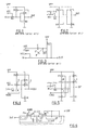
- the inverter of Fig. 1 operates as follows.
- the node A is similarly low because the transistor P2 is usually much more resistive than the driver (not shown in the figure) which drives the signal applied to the input IN, and therefore the voltage at the output OUT rises to a VPP value (which at the transition instant is equal to the supply voltage VCC of the general circuitry), thus cutting-off the transistor P2 and confirming the logic zero on the node A.
- the input IN becomes high (i.e.
- the latch circuit of Fig. 2 operates substantially in a way similar to that of the inverter circuit of Fig. 1, with the difference that the transistor N3 is made conducting by means of an appropriate sampling signal which is applied to the relative terminal only when the signal present at the input terminal IN of the circuit must be sampled, after which the latter signal remains stored in the circuit also after transistor N3 is cut off, being confirmed to a logic value "0" or to the logic value "1" by means of the transistor N4 or the transistor P2, respectively.
- junctions of the p-channel transistors P2 and P1 may be subject to breakdown when the voltage VPP assumes its maximum value (gated breakdown).
- a solution which is commonly resorted to for overcoming the gated breakdown problem of p-channel transistors is the so called "charge pump load".
- This circuit is depicted in Fig. 3 and utilizes only n-channel transistors and requires a timimg signal (phase) and therefore an oscillator for generating the latter for pumping electric charge on the output node OUT through the capacitor C and the diode connected transistor D1.
- Another disadvantage is that the output voltage is affected by the thresholds of the transistors D1 and T1 and becomes dependent also from the ratio between the capacitance C and the parasitic capacitance C′ toward the substrate.
- CMOS circuits of the prior art p-channel transistors which are subject to the VPP voltage must necessarily be provided with implanted drain-extension regions and, more in general, special processing techniques must be resorted to in order to make these p-channel transistors capable of withstanding such a high voltage (VPP).
- VPP high voltage
- the circuit object of the present invention provides a technique for preventing gated breakdown of junctions of p-channel transistors subject to a relatively high supply voltage VPP in these CMOS circuits, while permitting the use of a normal CMOS fabrication process not requiring the realization of drain-extension implantations in p channel transistors and not requiring the use of oscillators for pumping electric charge.
- the circuit of the invention employes a p-channel decoupling transistor connected substantially in series with the p-channel transistor of the CMOS circuit, be the latter for instance an inverter or a latch, for effectively preventing breakdown.
- This additional decoupling transistor is driven by a dedicated signal which may advantageously be a fraction of the VPP supply voltage suitably derived therefrom by means of a plurality of diodes or of diode-connected transistors connected in series between the VPP node and the gate of such a decoupling transistor.
- the inverter for operation at high voltabe of the present invention depicted in Fig. 4 shows a basic diagram substantially similar to the basic diagram of the prior art inverter depicted in Fig. 1 with the exception of the two additional p-channel transistors P5 and P6; similarly the latch for high voltage operation of the present invention depicted in Fig. 5 has a basic diagram which is substantially similar to the basic diagram of the prior art latch depicted in Fig. 2 with the exception of the two additional p-channel transistors P6 and P7.
- decoupling additional p-channel transistors (P5 and P6 in the case of the inverter of Fig. 4 and P7 and P6 in the case of the latch of Fig. 5) are connected in series with the p-channel transistors which are connected to the high voltage supply node VPP (P2 and P1). These decoupling p-channel additional transistors are driven through a dedicated terminal NOBD.
- the voltage of the NOBD terminal may be easily made to trail the VPP voltage by maintaining a certain potential difference between the VPP voltage and the NOBD terminal voltage for example by connecting the NOBD terminal to the VPP node through a series of diodes e.g. of diode-connected transistors.
- CMOS circuit of the invention is depicted in the cross section shown in Fig. 6.
- the n-well of the p-channel transistors P1 and P6, shown in the partial cross section of Fig. 6, is common and is connected to the VPP voltage.
- the C diffusion corresponding to the C node of the circuits depicted in Figures 4 and 5, is capacitively coupled through the capacitances C1, C2 and C3 to the gate of the transistor P6, to the n-well and to the gate of the transistor P1, respectively and, as observed before, the NOBD terminal is forced to ground potential before the VPP voltage begins to rise to its maximum asymptotic value.
- VNOBD C1 + VPP C2 / C1 + C2 + C3 as long as the diffusion remains substantially floating.
- C node of the depicted circuits Whenever the potential of such a C diffusion (C node of the depicted circuits) becomes greater than the voltage of the NOBD terminal increased by a voltage equal to the threshold of the transistor P6, the latter would start to conduct and to drag the potential of the C node toward the potential of the output node OUT, i.e. to ground, with the ultimate effect of cutting off itself. Therefore the C node maintains itself at a voltage which cannot become greater than the sum of the NOBD voltage and of the p-channel transistor threshold voltage.
- the C node voltage does not drop substantially below the sum of the NOBD voltage and of the p-channel threshold voltage because of the leakage of the p+/n-well junction, and cannot rise above such a value because of the attendant turning ON of the transistor P6.
- the leakage of the C diffusion may not be capable of positively preventing the potential of the node itself to drop and therefore to reach a breakdown condition, the resulting breakdown will immediately bring back the diffusion, i.e. the C node, to the above-noted operating voltage.
- Such a breakdown would not be a destructive breakdown because it is not supported by any constant current.
- the transistor P1 cannot ever reach the critical conditions of the so called gated breakdown because its drain is no longer at ground potential as it would without the presence of the coupling transistor P6 but, for instance, at about 9 V.
- the decoupling circuit arrangement of the present invention may be used in CMOS circuits every time there is a danger of originating a gated breakdown, i.e. in presence of relatively high supply voltages and when a normal CMOS fabrication process unable to produce p-channel type devices capable of withstanding relatively high voltage must be employed.
Landscapes
- Physics & Mathematics (AREA)
- Engineering & Computer Science (AREA)
- Computer Hardware Design (AREA)
- Computing Systems (AREA)
- General Engineering & Computer Science (AREA)
- Mathematical Physics (AREA)
- Metal-Oxide And Bipolar Metal-Oxide Semiconductor Integrated Circuits (AREA)
- Logic Circuits (AREA)
Applications Claiming Priority (2)
| Application Number | Priority Date | Filing Date | Title |
|---|---|---|---|
| IT8364688 | 1988-07-06 | ||
| IT8883646A IT1225607B (it) | 1988-07-06 | 1988-07-06 | Circuito logico cmos per alta tensione |
Publications (2)
| Publication Number | Publication Date |
|---|---|
| EP0350461A2 true EP0350461A2 (fr) | 1990-01-10 |
| EP0350461A3 EP0350461A3 (fr) | 1990-12-27 |
Family
ID=11323604
Family Applications (1)
| Application Number | Title | Priority Date | Filing Date |
|---|---|---|---|
| EP19890830290 Withdrawn EP0350461A3 (fr) | 1988-07-06 | 1989-06-23 | Circuit logique CMOS apte à fonctionner sous des tensions élevées |
Country Status (4)
| Country | Link |
|---|---|
| US (1) | US4956569A (fr) |
| EP (1) | EP0350461A3 (fr) |
| JP (1) | JPH0265270A (fr) |
| IT (1) | IT1225607B (fr) |
Cited By (3)
| Publication number | Priority date | Publication date | Assignee | Title |
|---|---|---|---|---|
| EP0509632A3 (en) * | 1991-04-19 | 1993-06-30 | Actel Corporation | Circuits for preventing breakdown of low-voltage device inputs during high voltage antifuse programming |
| EP0525939A3 (en) * | 1991-07-31 | 1993-07-07 | Actel Corporation | Methods for protecting outputs of low-voltage circuits from high programming voltages |
| EP0575188A1 (fr) * | 1992-06-17 | 1993-12-22 | Aptix Corporation | Cellule de mémoire de haute tension à accès aléatoire incorporant circuit de décalage de niveau |
Families Citing this family (12)
| Publication number | Priority date | Publication date | Assignee | Title |
|---|---|---|---|---|
| US5214322A (en) * | 1991-07-15 | 1993-05-25 | Unitrode Corporation | High voltage cmos power driver |
| JP3160449B2 (ja) * | 1993-12-02 | 2001-04-25 | 株式会社東芝 | トランジスタ回路 |
| US5493244A (en) * | 1994-01-13 | 1996-02-20 | Atmel Corporation | Breakdown protection circuit using high voltage detection |
| US5465054A (en) * | 1994-04-08 | 1995-11-07 | Vivid Semiconductor, Inc. | High voltage CMOS logic using low voltage CMOS process |
| US5483179A (en) * | 1994-04-20 | 1996-01-09 | International Business Machines Corporation | Data output drivers with pull-up devices |
| US5973956A (en) * | 1995-07-31 | 1999-10-26 | Information Storage Devices, Inc. | Non-volatile electrically alterable semiconductor memory for analog and digital storage |
| US5604449A (en) * | 1996-01-29 | 1997-02-18 | Vivid Semiconductor, Inc. | Dual I/O logic for high voltage CMOS circuit using low voltage CMOS processes |
| US5963076A (en) * | 1997-04-14 | 1999-10-05 | Motorola, Inc. | Circuit with hot-electron protection and method |
| US6351157B1 (en) | 1997-08-18 | 2002-02-26 | Vantis Corporation | Output buffer for making a high voltage (5.0 volt) compatible input/output in a low voltage (2.5 volt) semiconductor process |
| US6072351A (en) * | 1997-08-18 | 2000-06-06 | Advanced Micro Devices, Inc. | Output buffer for making a 5.0 volt compatible input/output in a 2.5 volt semiconductor process |
| US6362653B1 (en) * | 2001-02-06 | 2002-03-26 | International Business Machines Corporation | High voltage tolerant receivers |
| JP3675771B2 (ja) | 2002-03-22 | 2005-07-27 | 日本発条株式会社 | ディスクドライブ用サスペンション |
Family Cites Families (14)
| Publication number | Priority date | Publication date | Assignee | Title |
|---|---|---|---|---|
| US4441172A (en) * | 1981-12-28 | 1984-04-03 | National Semiconductor Corporation | Semiconductor memory core program control circuit |
| US4490629A (en) * | 1982-05-10 | 1984-12-25 | American Microsystems, Inc. | High voltage circuits in low voltage CMOS process |
| NL8304256A (nl) * | 1983-12-09 | 1985-07-01 | Philips Nv | Halfgeleiderinrichting. |
| NL8304400A (nl) * | 1983-12-22 | 1985-07-16 | Philips Nv | Digitale geintegreerde schakeling met complementaire veldeffekttransistoren. |
| US4565932A (en) * | 1983-12-29 | 1986-01-21 | Motorola, Inc. | High voltage circuit for use in programming memory circuits (EEPROMs) |
| EP0204762B1 (fr) * | 1984-12-10 | 1991-02-27 | AT&T Corp. | Circuit logique integré |
| US4704547A (en) * | 1984-12-10 | 1987-11-03 | American Telephone And Telegraph Company, At&T Bell Laboratories | IGFET gating circuit having reduced electric field degradation |
| JPH0738583B2 (ja) * | 1985-01-26 | 1995-04-26 | 株式会社東芝 | 半導体集積回路 |
| US4689504A (en) * | 1985-12-20 | 1987-08-25 | Motorola, Inc. | High voltage decoder |
| US4736117A (en) * | 1986-11-14 | 1988-04-05 | National Semiconductor Corporation | VDS clamp for limiting impact ionization in high density CMOS devices |
| FR2607338A1 (fr) * | 1986-11-21 | 1988-05-27 | Eurotechnique Sa | Circuit de commutation de tension en technologie mos |
| JPH0632230B2 (ja) * | 1987-03-31 | 1994-04-27 | 株式会社東芝 | 半導体不揮発性記憶装置 |
| US4845381A (en) * | 1987-10-01 | 1989-07-04 | Vlsi Technology, Inc. | Voltage level shifting circuit |
| US4820941A (en) * | 1988-02-01 | 1989-04-11 | Texas Instruments Incorporated | Decoder driver circuit for programming high-capacitance lines |
-
1988
- 1988-07-06 IT IT8883646A patent/IT1225607B/it active
-
1989
- 1989-06-23 EP EP19890830290 patent/EP0350461A3/fr not_active Withdrawn
- 1989-06-30 US US07/373,203 patent/US4956569A/en not_active Expired - Lifetime
- 1989-07-06 JP JP1175408A patent/JPH0265270A/ja active Pending
Cited By (4)
| Publication number | Priority date | Publication date | Assignee | Title |
|---|---|---|---|---|
| EP0509632A3 (en) * | 1991-04-19 | 1993-06-30 | Actel Corporation | Circuits for preventing breakdown of low-voltage device inputs during high voltage antifuse programming |
| EP0525939A3 (en) * | 1991-07-31 | 1993-07-07 | Actel Corporation | Methods for protecting outputs of low-voltage circuits from high programming voltages |
| US5341030A (en) * | 1991-07-31 | 1994-08-23 | Actel Corporation | Methods for protecting outputs of low-voltage circuits from high programming voltages |
| EP0575188A1 (fr) * | 1992-06-17 | 1993-12-22 | Aptix Corporation | Cellule de mémoire de haute tension à accès aléatoire incorporant circuit de décalage de niveau |
Also Published As
| Publication number | Publication date |
|---|---|
| IT1225607B (it) | 1990-11-22 |
| US4956569A (en) | 1990-09-11 |
| EP0350461A3 (fr) | 1990-12-27 |
| IT8883646A0 (it) | 1988-07-06 |
| JPH0265270A (ja) | 1990-03-05 |
Similar Documents
| Publication | Publication Date | Title |
|---|---|---|
| US4956569A (en) | CMOS logic circuit for high voltage operation | |
| EP0530159B1 (fr) | Circuit de remise à zéro à la mise sous tension à consommation nulle | |
| EP0485016B1 (fr) | Circuit de pompe à charge intégré à tension de rétropolarisation réduite | |
| US5321324A (en) | Low-to-high voltage translator with latch-up immunity | |
| US5128560A (en) | Boosted supply output driver circuit for driving an all N-channel output stage | |
| US5243236A (en) | High voltage CMOS switch with protection against diffusion to well reverse junction breakdown | |
| US5473268A (en) | Intermediary circuit between a low voltage logic circuit and a high voltage output stage in standard CMOS technology | |
| KR960003529B1 (ko) | 반도체 메모리 장치의 칩 초기화 신호 발생회로 | |
| US6184741B1 (en) | Bidirectional charge pump generating either a positive or negative voltage | |
| JP2869791B2 (ja) | 半導体集積回路装置およびそれを応用した電子装置 | |
| US4797584A (en) | Power-on reset circuit for MOS logic devices | |
| US4945267A (en) | Integrated circuit bus switching circuit | |
| JPS63307771A (ja) | 相補型金属酸化物半導体集積回路 | |
| EP0174694B1 (fr) | Circuit générant une tension de polarisation de substrat | |
| US5764097A (en) | Automatically biased voltage level converter | |
| US5552731A (en) | Integrated control circuit with a level shifter for switching an electronic switch | |
| JP2575956B2 (ja) | 基板バイアス回路 | |
| US20020067201A1 (en) | Driver timing and circuit technique for a low noise charge pump circuit | |
| KR100891909B1 (ko) | 반도체 장치 | |
| US7633332B2 (en) | Boosting circuit and boosting method | |
| JPH09167958A (ja) | 混合電圧システムのための出力ドライバ | |
| US6046617A (en) | CMOS level detection circuit with hysteresis having disable/enable function and method | |
| EP0215429A1 (fr) | Générateur de polarisation de substrat | |
| JP2704459B2 (ja) | 半導体集積回路装置 | |
| KR20060079755A (ko) | 파워 다운 및 과전압 허용 한계를 가진 버스 홀드 회로 |
Legal Events
| Date | Code | Title | Description |
|---|---|---|---|
| PUAI | Public reference made under article 153(3) epc to a published international application that has entered the european phase |
Free format text: ORIGINAL CODE: 0009012 |
|
| AK | Designated contracting states |
Kind code of ref document: A2 Designated state(s): DE FR GB NL SE |
|
| PUAL | Search report despatched |
Free format text: ORIGINAL CODE: 0009013 |
|
| AK | Designated contracting states |
Kind code of ref document: A3 Designated state(s): DE FR GB NL SE |
|
| 17P | Request for examination filed |
Effective date: 19910523 |
|
| 17Q | First examination report despatched |
Effective date: 19930729 |
|
| STAA | Information on the status of an ep patent application or granted ep patent |
Free format text: STATUS: THE APPLICATION HAS BEEN WITHDRAWN |
|
| 18W | Application withdrawn |
Withdrawal date: 19940126 |