EP0350940A2 - Procédé et dispositif pour la fabrication d'un milieu d'enregistrement magnétique - Google Patents
Procédé et dispositif pour la fabrication d'un milieu d'enregistrement magnétique Download PDFInfo
- Publication number
- EP0350940A2 EP0350940A2 EP89112903A EP89112903A EP0350940A2 EP 0350940 A2 EP0350940 A2 EP 0350940A2 EP 89112903 A EP89112903 A EP 89112903A EP 89112903 A EP89112903 A EP 89112903A EP 0350940 A2 EP0350940 A2 EP 0350940A2
- Authority
- EP
- European Patent Office
- Prior art keywords
- target
- substrate
- layer
- intermediate electrode
- sputtering
- Prior art date
- Legal status (The legal status is an assumption and is not a legal conclusion. Google has not performed a legal analysis and makes no representation as to the accuracy of the status listed.)
- Granted
Links
Images



Classifications
-
- G—PHYSICS
- G11—INFORMATION STORAGE
- G11B—INFORMATION STORAGE BASED ON RELATIVE MOVEMENT BETWEEN RECORD CARRIER AND TRANSDUCER
- G11B5/00—Recording by magnetisation or demagnetisation of a record carrier; Reproducing by magnetic means; Record carriers therefor
- G11B5/84—Processes or apparatus specially adapted for manufacturing record carriers
-
- G—PHYSICS
- G11—INFORMATION STORAGE
- G11B—INFORMATION STORAGE BASED ON RELATIVE MOVEMENT BETWEEN RECORD CARRIER AND TRANSDUCER
- G11B5/00—Recording by magnetisation or demagnetisation of a record carrier; Reproducing by magnetic means; Record carriers therefor
- G11B5/84—Processes or apparatus specially adapted for manufacturing record carriers
- G11B5/851—Coating a support with a magnetic layer by sputtering
-
- G—PHYSICS
- G11—INFORMATION STORAGE
- G11B—INFORMATION STORAGE BASED ON RELATIVE MOVEMENT BETWEEN RECORD CARRIER AND TRANSDUCER
- G11B5/00—Recording by magnetisation or demagnetisation of a record carrier; Reproducing by magnetic means; Record carriers therefor
- G11B5/84—Processes or apparatus specially adapted for manufacturing record carriers
- G11B5/8404—Processes or apparatus specially adapted for manufacturing record carriers manufacturing base layers
Definitions
- the present invention relates to a method for producing a magnetic recording medium. Particularly, it relates to a method for producing a magnetic recording medium having a high coercive force.
- the coercive force of a thin cobalt alloy magnetic layer increases with the thickness of the chromium undercoating layer.
- the coercive force shows a saturation characteristic, and it becomes difficult to further increase the coercive force.
- Japanese Unexamined Patent Publication No. 79968/1988 teaches that when the thickness of a thin chromium undercoating layer exceeds 1,500 ⁇ , a saturation tendency is observed such that the coercive force of the magnetic layer no longer increases, and when the thickness of the undercoating layer is less than 1,500 ⁇ , the coercive force tends to be remarkably low at a practically useless level.
- the coercive force increases with a reduction of the thickness of the thin cobalt alloy layer.
- the reduction of the thickness of the cobalt alloy layer leads to a decrease in the reproduction output, and it is practically difficult to reduce the thickness beyond a certain level.
- the coercive force may be increased to some extent by selecting the sputtering conditions such as the pressure of the gas for forming or the substrate temperature during the formation of the magnetic layer, but such improvement is limited.
- the present inventors have conducted extensive researches to improve the coercive force of the magnetic recording medium.
- the coercive force of the magnetic recording medium can be remarkably improved by providing an intermediate electrode in the vicinity of the circumference of the target and forming a thin undercoating layer and/or a thin metal magnetic layer on a substrate by sputtering while applying a positive potential to the intermediate electrode relative to the grounded portion of the main body of the layer-forming apparatus.
- the present invention has been accomplished on the basis of this discovery.
- the present invention provides a method for producing a magnetic recording medium, which comprises forming, by sputtering, a thin undercoating layer and a thin cobalt alloy magnetic layer sequentially on a substrate, wherein an intermediate electrode is provided in the vicinity of the target to enclose at least 1/2 of the circumference of the sputter erosion end of the target, and at least one of the undercoating layer and the cobalt alloy magnetic layer is formed under such condition that a positive potential relative to the substrate and the grounded portion of the main body of the layer-forming apparatus, is applied to the intermediate electrode.
- the present invention also provides a sputtering apparatus for forming a thin layer on a substrate by sputtering, which comprises an intermediate electrode disposed in the vicinity of a target provided to face the substrate and having a shape to enclose at least 1/2 of the circumference of the sputter erosion end of the target and a power source to apply a positive potential to the intermediate electrode.
- a disk substrate made of a metal, particularly aluminum or an aluminum alloy is usually employed. It is usual to employ the one prepared by processing an aluminum substrate to a prescribed thickness, then treating the surface for specular finish, forming a first undercoating layer of a hard non-magnetic metal such as a Ni-P alloy by electroless plating or by anodic oxidation treatment, and then sputtering chromium as a second undercoating layer. As the substrate, it is also possible to employ the one prepared by sputtering chromium as an undercoating layer directly on an aluminum substrate treated for specular finish without forming the above-mentioned first undercoating layer.
- the sputtering condition for forming the chromium undercoating layer there is no particular restriction as to the sputtering condition for forming the chromium undercoating layer. It is possible to employ sputtering conditions commonly used for forming a usual chromium undercoating layer or sputtering conditions as described hereinafter for the formation of a thin magnetic layer.
- the thickness of the chromium undercoating layer is usually within a range of from 1,000 to 3,000 ⁇ in view of the relation to the coercive force of the magnetic layer.
- the magnetic layer is made of a Co-Cr-Ta alloy
- a high coercive force can be obtained even when the thickness of the chromium undercoating layer is less than 1,000 ⁇ , and in this case, the thickness may be within a range of from 50 to 1,000 ⁇ .
- the thin chromium undercoating layer and/or the thin cobalt alloy magnetic layer is formed on the substrate by sputtering under the specific condition.
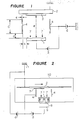
- Figure 1 is a diagrammatical view illustrating an embodiment of the sputtering apparatus of the present invention.
- reference numeral 1 indicates a target, and a substrate holder 2 is provided to face the target.
- a substrate 3 is mounted on the substrate holder 2.
- the substrate holder 2 is movable so that the substrate 3 can be continuously subjected to the layer-forming operation.
- An intermediate electrode 4 is disposed in a shape to enclose the space for sputtering discharge between this target 1 and the substrate 2, more particularly, in a shape to enclose at least 1/2 of the circumference of the sputter erosion end of the target 1 in the vicinity of the target 1.
- Numeral 5 indicates a power source for sputtering, which is connected to the target 1 and the intermediate electrode 4.
- Numeral 6 indicates a power source for the intermediate electrode, which is connected to the grounded portion of the main body of the layer-forming apparatus and the intermediate electrode 4.
- Numeral 7 indicates the sputter erosion portion of the target 1.
- the sputtering power source 5 and the intermediate electrode power source 6 are preferably direct current power sources. However, RF power sources may also be employed. As the sputtering apparatus, a usual DC magnetron sputtering apparatus or RF magnetron sputtering apparatus may be employed.
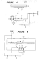
- Figure 2 is a detailed view of the sputtering apparatus of Figure 1.
- Numeral 8 indicates a magnet for magnetron, numeral 9 a cathode of the DC magnetron, numeral 10 the main body of the layer-forming apparatus, and numeral 11 the grounded portion of the main body 10 of layer-forming apparatus.
- Figures 3(A) to 3(F) are cross sectional views illustrating the positions and shapes of intermediate electrodes 4 of the present invention.
- the electrode 4 is in a shape to enclose at least 1/2 of the circumference of the sputter erosion end of the target 1.
- the intermediate electrode 4 is located between a position distanced by 1/3, preferably 1/4, of the distance between the surface of the target and the surface of the substrate, from the surface of the target in a direction towards the substrate, and a position distanced by 30 mm, preferably 20 mm, from the surface of the target in a direction away from the substrate.
- the intermediate electrode 4 is located between the circumference of the sputter erosion end of the target and a position distanced by 200 mm, preferably 150 mm, more preferably 120 mm, from said circumference outwardly in the plane of the target, in a shape to enclose at least 1/2 of the circumference of the sputter erosion end of the target, preferably the entire circumference of the target.
- the intermediate electrode 4 is located between a position distanced by 30 mm from the surface of the target in a direction towards the substrate and a position distanced by 20 mm from the surface of the target in a direction away from the substrate, and between the circumference of the target and a position distanced by 120 mm from said circumference outwardly in the plane of the target in a shape to enclose the entire circumference of the target.
- the shape of the intermediate electrode 4 a shape to enclose at least 1/2 of the circumference of the target 1, such as a ring shape, a cylindrical shape or a sheet shape, is employed. If the intermediate electrode encloses less than 1/2 of the circumference of the target 1, the effects for improving the coercive force tend to be low, such being undesirable.
- the intermediate electrode is made usually of a metal such as stainless steel, aluminum or copper.
- the sputter erosion end of the target is meant for a boundary between the sputtered area (sputter erosion portion) and the non-sputtered area when the surface of the target has been sputtered.
- the circumference of this boundary is defined as the circumference of the sputter erosion end of the target.
- the sputter erosion portion will have a ring shape having an inner circumference and an outer circumference. This outer circumference is regarded as the circumference of the sputter erosion end of the target in the present invention.
- the position of the sputter erosion end is determined by the size of the target and the position of the magnet for magnetron. In a case of a sputtering apparatus wherein the surface of the target is covered with a shield plate, the position of the sputter erosion end is determined by the size of such shield plate.
- a cobalt alloy containing cobalt as the main component such as Co-Cr, Co-Cr-X, Co-Ni-X, Co-W-X wherein X is at least one element selected from the group consisting of Li, Si, B, Ca, Ti, V, Cr, Ni, As, Y, Zr, Nb, Mo, Ru, Rh, Ag, Sb, Hf, Ta, W, Re, Os, Ir, Pt, Au, La, Ce, Pr, Nd, Pm, Sm and Eu, may be employed.
- an alloy comprising Co as the main component and Cr and Ta is preferably employed.
- This Co-Cr-Ta alloy preferably comprises from 70 to 95 atomic % of Co, from 5 to 20 atomic % of Cr and from 0.1 to 10 atomic % of Ta.
- sputtering is conducted under such condition that a positive potential relative to the substrate and the grounded portion of the main body of the sputtering apparatus, for example, a voltage of at most 1,000 V, preferably from 50 to 500 V, more preferably from 100 to 400 V, is applied to the intermediate electrode 4, to form a thin chromium undercoating layer or a thin cobalt alloy magnetic layer on the substrate 3.
- a positive potential relative to the substrate and the grounded portion of the main body of the sputtering apparatus for example, a voltage of at most 1,000 V, preferably from 50 to 500 V, more preferably from 100 to 400 V, is applied to the intermediate electrode 4, to form a thin chromium undercoating layer or a thin cobalt alloy magnetic layer on the substrate 3.
- the sputtering conditions may be those commonly employed for forming a magnetic layer of a magnetic recording medium.
- sputtering can be conducted under such conditions that the inner pressure of the evacuated chamber (background pressure) is at most 1 x 10 ⁇ 6 Torr, the pressure of a rare gas such as argon is from 0.5 x 10 ⁇ 3 to 2 x 10 ⁇ 2 Torr, preferably from 1 x 10 ⁇ 3 to 5 x 10 ⁇ 3 Torr, and the substrate temperature is at least 150°C, preferably from 200 to 300°C.
- the thickness of the thin magnetic alloy layer formed by such sputtering is preferably at such a level that the product (Br ⁇ t) of the residual magnetic flux density (Br) and the thickness (t) of the thin magnetic alloy layer would be from 300 to 700 G ⁇ m.
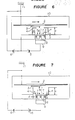
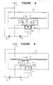
- Figures 4 to 13 are diagrammatical and detailed views of other embodiment of the sputtering apparatus suitable for the operation of the present invention.
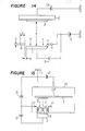
- Figures 14 and 15 are diagrammatical and detailed views illustrating still another embodiment of the sputtering apparatus useful for the operation of the present invention, in which reference numeral 12 is a bias power source to apply a negative bias voltage to the substrate holder 2.
- reference numeral 12 is a bias power source to apply a negative bias voltage to the substrate holder 2.
- the above-mentioned substrate 3 is mounted on the substrate holder 2, and sputtering is conducted by using the above-mentioned chromium or cobalt alloy target 1 in the presence of a rare gas such as Ar.
- sputtering is conducted under such condition that a positive potential relative to the substrate and the grounded portion of the main body of the sputtering apparatus, for example, a potential of at most 1,000 V, preferably from 50 to 500 V, more preferably from 100 to 400 V, is applied to the intermdiate electrode 4.
- sputtering is conducted in such state that a negative bias voltage is applied to the substrate holder 2, i.e. a voltage of e.g. at least -1,000 V, preferably from -50 to -500 V, more preferably from -100 to -400 V, is applied to the substrate holder 2 by the bias power source 12, to form a thin chromium undercoating layer or a thin cobalt alloy magnetic layer on the substrate 3.
- a negative bias voltage is applied to the substrate holder 2, i.e. a voltage of e.g. at least -1,000 V, preferably from -50 to -500 V, more preferably from -100 to -400 V, is applied to the substrate holder 2 by the bias power source 12, to form a thin chromium undercoating layer or a thin cobalt alloy magnetic layer on the substrate 3.
- a high performance magnetic layer having a high coercive force is obtained by the thin magnetic metal layer of a cobalt alloy formed by sputtering under such condition that the intermediate electrode is provided in the vicinity of the circumference of the target and a positive potential relative to the substrate and the grounded portion of the main body of the layer-forming apparatus is applied to the intermediate electrode.
- the substrate holder 2 is grounded via the main body 10 of the layer-forming apparatus.
- sputtering was conducted by using an aluminum substrate 3 having a thin chromium layer (thickness: 1,000 ⁇ ) as the undercoating layer and a Co-Cr-Ta alloy target 1 under such condition that a positive potential as identified in Table 1 relative to the substrate was applied to the intermediate electrode 4 in the presence of Ar gas at a background pressure of at most 1 x 10 ⁇ 6 Torr, at an argon gas pressure of 4 x 10 ⁇ 3 Torr and at a substrate temperature of 210°C, to form an 86 atomic % Co-12 atomic % Cr-2 atomic % Ta magnetic layer (400 G ⁇ m) on the substrate.
- Ar gas at a background pressure of at most 1 x 10 ⁇ 6 Torr, at an argon gas pressure of 4 x 10 ⁇ 3 Torr and at a substrate temperature of 210°C
- Shape a shape to enclose the entire circumference of the target.
- sputtering was conducted by using an aluminum substrate 3 having a thin chromium layer (thickness: 1,000 ⁇ ) formed as the undercoating layer by sputtering and a Co-Cr-Ta alloy target 1 under such condition that a potential as identified in Table 2 relative to the substrate 3 was applied to the intermediate electrode 4 at a background pressure of at most 1 x 10 ⁇ 6 Torr, at an argon gas pressure of 2 x 10 ⁇ 3 Torr and at a substrate temperature of 250°C, to form an 86 atomic % Co-12 atomic % Cr-2 atomic % Ta magnetic layer (550 G ⁇ m) on the substrate.
- the coercive force of the magnetic disk thus obtained was measured by a sample vibrating type magnetometer, and the results are shown in Table 2.
- Shape a shape to enclose the entire circumference of the target.
- Example 8 50 1100
- Example 9 100 1160
- Example 10 150 1260
- Example 11 200 1350
- Example 12 300 1380
- sputtering was sequentially conducted by using an aluminum substrate 3 and a chromium target and a Co-Cr-Ta alloy target under such condition that a potential as identified in Table 3 relative to the substrate 3 was applied to the intermediate electrode 4 at the background pressure of at most 1 x 10 ⁇ 6 Torr, at an argon gas pressure of 2 x 10 ⁇ 3 Torr and at a substrate temperature of 250°C to sequentially form a chromium layer (thickness: 1,000 ⁇ ) and an 86 atomic % Co-12 atomic % Cr-2 atomic % Ta magnetic layer (550 G ⁇ m) on the substrate.
- sputtering was conducted by using an aluminum substrate 3 having a thin chromium layer (thickness: 1,000 ⁇ ) formed as the undercoating layer by sputtering and a Co-Cr-Ta alloy target 1 under such condition that a potential as identified in Table 4 relative to the substrate 3 was applied to the intermediate electrode 4 at a background pressure of at most 1 x 10 ⁇ 6 Torr, at an argon gas pressure of 2 x 10 ⁇ 3 Torr and at a substrate temperature of 250°C, to form an 86 atomic % Co-12 atomic % Cr-2 atomic % Ta magnetic layer (550 G ⁇ m) on the substrate.
- sputtering was conducted by using an aluminum substrate 3 having a thin chromium layer (thickness: 1,000 ⁇ ) formed as the undercoating layer and a Co-Cr-Ta alloy target 1 under such condition that a potential as identified in Table 5 was applied to the intermediate electrode 4 at a background pressure of at most 1 x 10 ⁇ 6 Torr, at an argon gas pressure of 2 x 10 ⁇ 3 Torr and at a substrate temperature of 250°C, to form an 86 atomic % Co-12 atomic % Cr-2 atomic % Ta magnetic layer (550 G ⁇ m) on the substrate.
- the coercive force of the magnetic disk thus obtained was measured by a sample vibrating type magnetometer, and the results are shown in Table 5.
- sputtering was conducted by using an aluminum substrate 3 having a thin chromium layer (thickness: 1,000 ⁇ ) formed as the undercoating layer by sputtering and a Co-Cr-Ta alloy target 1 under such condition that a potential as identified in Table 6 relative to the substrate 3 was applied to the intermediate electrode 4 at a background pressure of at most 1 x 10 ⁇ 6 Torr, at an argon gas pressure of 2 x 10 ⁇ 3 Torr and at a substrate temperature of 250°C, to form an 86 atomic % Co-12 atomic % Cr-2 atomic % Ta magnetic layer (550 G ⁇ m) on the substrate.
- the coercive force of the magnetic disk thus obtained was measured by a sample vibrating type magnetometer, and the results are shown in Table 6.
- sputtering was conducted by using an aluminum substrate 3 having a thin chromium layer (thickness: 1,000 ⁇ ) formed as the undercoating layer by sputtering and a Co-Cr-Ta alloy target 1 under such condition that a potential as identified in Table 7 relative to the substrate 3 was applied to the intermediate electrode 4 at a background pressure of at most 1 x 10 ⁇ 6 Torr, at an argon gas pressure of 2 x 10 ⁇ 3 Torr and at a substrate temperature of 250°C, to form an 86 atomic % Co-12 atomic % Cr-2 atomic % Ta magnetic layer (550 G ⁇ m) on the substrate.
- Shape in Examples 29 and 30 a shape to enclose the entire circumference of the target
- Example 31 a shape to enclose 60% of the circumference of the target.
- Table 7 Magnetic layer Voltage applied to intermediate electrode (V) Coercive force (Oe) Comparative Example 7 Co86-Cr12-Ta2 0 950
- Example 29 200 1150
- Example 30 300 1080
- Example 31 200 1050
- sputtering was conducted by using an aluminum substrate 3 having a thin chromium layer (thickness: 1,000 ⁇ ) formed as the undercoating layer by sputtering and a Co-Cr-Ta alloy target 1 under such condition that a potential as identified in Table 8 relative to the substrate 3 was applied to the intermediate electrode 4 at a background pressure of at most 1 x 10 ⁇ 6 Torr, at an argon gas pressure of 2 x 10 ⁇ 3 Torr and at a substrate temperature of 250°C, to form an 86 atomic % Co-12 atomic % Cr-2 atomic % Ta magnetic layer (550 G ⁇ m) on the substrate.
- sputtering was conducted by using an aluminum substrate 3 having a thin chromium layer (thickness: 1,000 ⁇ ) formed as the undercoating layer by sputtering and a Co-Cr-Ta alloy target 1 under such condition that a potential as identified in Table 9 relative to the substrate 3 was applied to the intermediate electrode 4 at a background pressure of at most 1 x 10 ⁇ 6 Torr, at an argon gas pressure of 2 x 10 ⁇ 3 Torr and at a substrate temperature of 250°C, to form an 86 atomic % Co-12 atomic % Cr-2 atomic % Ta magnetic layer (550 G ⁇ m) on the substrate.
- sputtering was conducted by using an aluminum substrate 3 having a thin chromium layer with a thickness as identified in table 10 formed as the undercoating layer by sputtering and a Co-Cr-Ta alloy target 1 under such a condition that a potential as identified in Table 10 relative to the substrate 3 was applied to the intermediate electrode 4 at a background pressure of at most 1 x 10 ⁇ 6 Torr, at an argon gas pressure of 2 x 10 ⁇ 3 Torr and at a substrate temperature of 250°C, to form an 86 atomic % Co-12 atomic % Cr-2 atomic % Ta magnetic layer (550 G ⁇ m) on the substrate.
- the coercive force of the magnetic disk thus obtained was measured by a sample vibrating type magnetometer, and the results are shown in Table 10.
- a magnetic disk was prepapred in the same manner as in Example 33 except that a Co-Ni-Cr alloy target was used instead of the Co-Cr-Ta alloy target and a 70 atomic % Co-20 atomic % Ni-10 atomic % Cr magnetic layer (550 G ⁇ m) was formed on the substrate at the voltage as shown in Table 10. The coercive force was measured, and the results are shown in Table 10.
- sputtering was conducted by using an aluminum substrate 3 having a thin chromium layer (thickness: 2,000 ⁇ ) formed as the undercoating layer by sputtering and a cobalt alloy target 1 having the composition as identified in Table 11 under such condition that a potential as identified in Table 11 relative to the substrate 3 was applied to the intermediate electrode 4 at a background pressure of at most 1 x 10 ⁇ 6 Torr, at an argon gas pressure of 2 x 10 ⁇ 3 Torr and at a substrate temperature of 250°C, to form a magnetic layer as identified in Table 11 (550 G ⁇ m) on the substrate.
- sputtering was conducted by using an aluminum substrate 3 having a thin chromium layer (thickness: 2,000 ⁇ ) formed as the undercoating layer and a Co-Cr-Ta alloy target 1 under such condition that a potential as identified in Table 12 was applied to the intermediate electrode 4 at a background pressure of at most 1 x 10 ⁇ 6 Torr, at an argon gas pressure of 2 x 10 ⁇ 3 Torr and at a substrate temperature of 250°C, to form an 86 atomic % Co-12 atomic % Cr-2 atomic % Ta magnetic layer (400 G ⁇ m) on the substrate.
- the coercive force of the magnetic disk thus obtained was measured by a sample vibrating type magnetometer, and the results are shown in Table 12.
- Shape a shape to enclose the entire circumference of the target.
- Example 43 Magnetic layer Voltage applied to intermediate electrode (V) Coercive force (Oe) Comparative Example 25 Co86-Cr12-Ta2 0 940
- Example 43 100 1380
- Example 44 200 1500
- Example 45 300
- Example 46 400
- Comparative Example 26 Co86-Cr9-Ag5 0 750
- Example 47 250 1100 Comparative Example 27 Co67-Ni30-B3 0 890
- Example 48 250 1240
- sputtering was conducted by using an aluminum substrate 3 having a thin chromium layer (thickness: 2,000 ⁇ ) formed as the undercoating layer by sputtering and a Co-Cr-Ta alloy target 1 under such condition that a potential as identified in Table 13 relative to the substrate 3 was applied to the intermediate electrode 4 at a background pressure of at most 1 x 10 ⁇ 6 Torr, at an argon gas pressure of 2 x 10 ⁇ 3 Torr and at a substrate temperature of 250°C, to form an 86 atomic % Co-12 atomic % Cr-2 atomic % Ta magnetic layer (400 G ⁇ m) on the substrate.
- sputtering was conducted by using an aluminum substrate 3 having a thin chromium layer (thickness: 2,000 ⁇ ) formed as the undercoating layer and a Co-Cr-Ta alloy target 1 under such condition that a potential as identified in Table 14 was applied to the intermediate electrode 4 and a voltage from the bias power source 12 as identified in Table 14 was applied to the substrate 3 at a background pressure of at most 1 x 10 ⁇ 6 Torr, at an argon gas pressure of 2 x 10 ⁇ 3 Torr and at a substrate temperature of 250°C, to form an 86 atomic % Co-12 atomic % Cr-2 atomic % Ta magnetic layer (400 G ⁇ m) on the substrate.
- the coercive force of the magnetic disk thus obtained was measured by a sample vibrating type magnetometer, and the results are shown in Table 14.
- Shape a shape to enclose the entire circumference of the target.
- Table 14 Voltage applied to intermediate electrode (V) Voltage applied from bias power source (V) Coercive force (Oe) Comparative Example 29 0 0 940
- Example 50 100 0 1380
- Example 51 200 0 1500
- Example 52 300 0 1550
- Example 53 400 0 1570 Comparative Example 30 0 -100 1380
- Example 54 100 -100 1550
- Example 55 200 -100 1590
- Example 56 300 -100 1610 Comparative Example 31 0 -200 1560
- Example 58 200 -200 1600 Comparative Example 32 0 -300 1580
- Example 59 100 -300 1600
Landscapes
- Engineering & Computer Science (AREA)
- Manufacturing & Machinery (AREA)
- Manufacturing Of Magnetic Record Carriers (AREA)
Applications Claiming Priority (6)
| Application Number | Priority Date | Filing Date | Title |
|---|---|---|---|
| JP17625588 | 1988-07-15 | ||
| JP176255/88 | 1988-07-15 | ||
| JP63317708A JPH02162527A (ja) | 1988-12-16 | 1988-12-16 | 磁気記録媒体の製造法 |
| JP63317704A JPH02162526A (ja) | 1988-12-16 | 1988-12-16 | 磁気記録媒体の製造方法 |
| JP317708/88 | 1988-12-16 | ||
| JP317704/88 | 1988-12-16 |
Publications (3)
| Publication Number | Publication Date |
|---|---|
| EP0350940A2 true EP0350940A2 (fr) | 1990-01-17 |
| EP0350940A3 EP0350940A3 (fr) | 1991-01-09 |
| EP0350940B1 EP0350940B1 (fr) | 1994-03-16 |
Family
ID=27324227
Family Applications (1)
| Application Number | Title | Priority Date | Filing Date |
|---|---|---|---|
| EP89112903A Expired - Lifetime EP0350940B1 (fr) | 1988-07-15 | 1989-07-13 | Procédé et dispositif pour la fabrication d'un milieu d'enregistrement magnétique |
Country Status (4)
| Country | Link |
|---|---|
| US (1) | US4997539A (fr) |
| EP (1) | EP0350940B1 (fr) |
| KR (1) | KR970002340B1 (fr) |
| DE (1) | DE68913837D1 (fr) |
Cited By (3)
| Publication number | Priority date | Publication date | Assignee | Title |
|---|---|---|---|---|
| EP0479232A1 (fr) * | 1990-10-01 | 1992-04-08 | Komag, Inc. | Alliage magnétique à base de cobalt, nickel, platine et chrome |
| US5492745A (en) * | 1989-04-04 | 1996-02-20 | Mitsubishi Chemical Corporation | Magnetic recording medium and method for its production |
| US12595550B2 (en) | 2022-02-18 | 2026-04-07 | Evatec Ag | Vacuum layer deposition apparatus and method of depositing a layer on a substrate, especially on a substrate comprising indentations in the surface to be coated |
Families Citing this family (15)
| Publication number | Priority date | Publication date | Assignee | Title |
|---|---|---|---|---|
| US5316645A (en) * | 1990-08-07 | 1994-05-31 | Canon Kabushiki Kaisha | Plasma processing apparatus |
| US5328583A (en) * | 1991-11-05 | 1994-07-12 | Canon Kabushiki Kaisha | Sputtering apparatus and process for forming lamination film employing the apparatus |
| USRE38544E1 (en) | 1994-01-28 | 2004-07-06 | Komag, Inc. | Thin film magnetic alloy having low noise, high coercivity and high squareness |
| JP2904263B2 (ja) * | 1995-12-04 | 1999-06-14 | 日本電気株式会社 | スパッタ装置 |
| ES2184265T3 (es) * | 1997-04-14 | 2003-04-01 | Cemecon Ag | Procedimiento y dispositivo de revestimiento por pvd. |
| US5891311A (en) * | 1997-06-25 | 1999-04-06 | Intevac, Inc. | Sputter coating system and method using substrate electrode |
| US6210819B1 (en) | 1998-07-24 | 2001-04-03 | Hmt Technology Corporation | Magnetic recording media having a CrTi underlayer deposited under a substrate bias |
| US8043484B1 (en) | 2001-03-13 | 2011-10-25 | Novellus Systems, Inc. | Methods and apparatus for resputtering process that improves barrier coverage |
| US6764940B1 (en) | 2001-03-13 | 2004-07-20 | Novellus Systems, Inc. | Method for depositing a diffusion barrier for copper interconnect applications |
| US6602800B2 (en) * | 2001-05-09 | 2003-08-05 | Asm Japan K.K. | Apparatus for forming thin film on semiconductor substrate by plasma reaction |
| US8298933B2 (en) * | 2003-04-11 | 2012-10-30 | Novellus Systems, Inc. | Conformal films on semiconductor substrates |
| US7842605B1 (en) | 2003-04-11 | 2010-11-30 | Novellus Systems, Inc. | Atomic layer profiling of diffusion barrier and metal seed layers |
| US7510634B1 (en) | 2006-11-10 | 2009-03-31 | Novellus Systems, Inc. | Apparatus and methods for deposition and/or etch selectivity |
| US7682966B1 (en) | 2007-02-01 | 2010-03-23 | Novellus Systems, Inc. | Multistep method of depositing metal seed layers |
| US7922880B1 (en) | 2007-05-24 | 2011-04-12 | Novellus Systems, Inc. | Method and apparatus for increasing local plasma density in magnetically confined plasma |
Family Cites Families (6)
| Publication number | Priority date | Publication date | Assignee | Title |
|---|---|---|---|---|
| US3410775A (en) * | 1966-04-14 | 1968-11-12 | Bell Telephone Labor Inc | Electrostatic control of electron movement in cathode sputtering |
| FR2324755A1 (fr) * | 1975-09-19 | 1977-04-15 | Anvar | Dispositif de pulverisation cathodique de grande vitesse de depot |
| NL8202092A (nl) * | 1982-05-21 | 1983-12-16 | Philips Nv | Magnetronkathodesputtersysteem. |
| JPS5916975A (ja) * | 1982-07-20 | 1984-01-28 | Canon Inc | スパツタリング装置 |
| DE3223245C2 (de) * | 1982-07-23 | 1986-05-22 | Nihon Shinku Gijutsu K.K., Chigasaki, Kanagawa | Ferromagnetische Hochgeschwindigkeits-Kathodenzerstäubungs-Vorrichtung |
| JPS63270461A (ja) * | 1986-12-26 | 1988-11-08 | Teijin Ltd | 対向ターゲット式スパッタ装置 |
-
1989
- 1989-07-11 KR KR1019890009884A patent/KR970002340B1/ko not_active Expired - Fee Related
- 1989-07-12 US US07/378,963 patent/US4997539A/en not_active Expired - Lifetime
- 1989-07-13 EP EP89112903A patent/EP0350940B1/fr not_active Expired - Lifetime
- 1989-07-13 DE DE89112903T patent/DE68913837D1/de not_active Expired - Lifetime
Cited By (4)
| Publication number | Priority date | Publication date | Assignee | Title |
|---|---|---|---|---|
| US5492745A (en) * | 1989-04-04 | 1996-02-20 | Mitsubishi Chemical Corporation | Magnetic recording medium and method for its production |
| EP0479232A1 (fr) * | 1990-10-01 | 1992-04-08 | Komag, Inc. | Alliage magnétique à base de cobalt, nickel, platine et chrome |
| US5180640A (en) * | 1990-10-01 | 1993-01-19 | Komag, Inc. | Magnetic recording medium comprising a magnetic alloy layer of cobalt nickel, platinum and chromium formed directly on a nickel alloy amorphous underlayer |
| US12595550B2 (en) | 2022-02-18 | 2026-04-07 | Evatec Ag | Vacuum layer deposition apparatus and method of depositing a layer on a substrate, especially on a substrate comprising indentations in the surface to be coated |
Also Published As
| Publication number | Publication date |
|---|---|
| EP0350940A3 (fr) | 1991-01-09 |
| US4997539A (en) | 1991-03-05 |
| DE68913837D1 (de) | 1994-04-21 |
| EP0350940B1 (fr) | 1994-03-16 |
| KR970002340B1 (ko) | 1997-03-03 |
| KR900002253A (ko) | 1990-02-28 |
Similar Documents
| Publication | Publication Date | Title |
|---|---|---|
| EP0350940B1 (fr) | Procédé et dispositif pour la fabrication d'un milieu d'enregistrement magnétique | |
| EP0054269B1 (fr) | Milieu d'enregistrement perpendiculaire magnétique, son procédé de fabrication et un dispositif de pulvérisation | |
| EP0388088A2 (fr) | Disque magnétique pour stocker des dates à bas niveau intrinsèque de bruit | |
| US5976326A (en) | Method of sputtering selected oxides and nitrides for forming magnetic media | |
| EP0391258A2 (fr) | Support d'enregistrement magnétique et méthode de fabrication | |
| EP0333101B1 (fr) | Procédé de fabrication d'un matériau d'enregistrement magnétique | |
| EP0710949B1 (fr) | Support d'enregistrement magnetique et sa fabrication | |
| JPH05274644A (ja) | 磁気記録媒体及びその製造方法 | |
| US6821618B2 (en) | Magnetic recording medium and process for producing the same | |
| EP0576376B1 (fr) | Film magnétique cobalt-platine et méthode de fabrication | |
| US6753077B2 (en) | Magnetic recording medium and process for producing the same | |
| US5294312A (en) | Method for preparing a magnetic recording medium | |
| JP2906453B2 (ja) | 磁気記録媒体製造用スパッタリング装置 | |
| JPH04134719A (ja) | 磁気記録媒体 | |
| EP0619585A1 (fr) | Matériaux magnétiquement doux en FeRhGaSi pour têtes magnétiques inductives | |
| Kawanabe et al. | Effects of Ta addition in CoNi/Cr double layer film sputtered in low Ar gas pressure | |
| US4410406A (en) | Process for preparing magnetic recording medium | |
| JP2973551B2 (ja) | 磁気記録媒体 | |
| JP2832941B2 (ja) | 面内磁気記録媒体 | |
| JPH0572015B2 (fr) | ||
| JPH0740342B2 (ja) | 磁気記録媒体及びその製造方法 | |
| JPH0526250B2 (fr) | ||
| KR920008436B1 (ko) | 자기기록체 | |
| JPH0740341B2 (ja) | 磁気記録媒体及びその製造方法 | |
| JPH0572016B2 (fr) |
Legal Events
| Date | Code | Title | Description |
|---|---|---|---|
| PUAI | Public reference made under article 153(3) epc to a published international application that has entered the european phase |
Free format text: ORIGINAL CODE: 0009012 |
|
| AK | Designated contracting states |
Kind code of ref document: A2 Designated state(s): DE GB IT |
|
| PUAL | Search report despatched |
Free format text: ORIGINAL CODE: 0009013 |
|
| AK | Designated contracting states |
Kind code of ref document: A3 Designated state(s): DE GB IT |
|
| 17P | Request for examination filed |
Effective date: 19901212 |
|
| 17Q | First examination report despatched |
Effective date: 19930511 |
|
| GRAA | (expected) grant |
Free format text: ORIGINAL CODE: 0009210 |
|
| AK | Designated contracting states |
Kind code of ref document: B1 Designated state(s): DE GB IT |
|
| PG25 | Lapsed in a contracting state [announced via postgrant information from national office to epo] |
Ref country code: DE Effective date: 19940316 |
|
| ITF | It: translation for a ep patent filed | ||
| REF | Corresponds to: |
Ref document number: 68913837 Country of ref document: DE Date of ref document: 19940421 |
|
| PLBE | No opposition filed within time limit |
Free format text: ORIGINAL CODE: 0009261 |
|
| STAA | Information on the status of an ep patent application or granted ep patent |
Free format text: STATUS: NO OPPOSITION FILED WITHIN TIME LIMIT |
|
| 26N | No opposition filed | ||
| PGFP | Annual fee paid to national office [announced via postgrant information from national office to epo] |
Ref country code: GB Payment date: 19990707 Year of fee payment: 11 |
|
| PG25 | Lapsed in a contracting state [announced via postgrant information from national office to epo] |
Ref country code: GB Free format text: LAPSE BECAUSE OF NON-PAYMENT OF DUE FEES Effective date: 20000713 |
|
| GBPC | Gb: european patent ceased through non-payment of renewal fee |
Effective date: 20000713 |
|
| PG25 | Lapsed in a contracting state [announced via postgrant information from national office to epo] |
Ref country code: IT Free format text: LAPSE BECAUSE OF NON-PAYMENT OF DUE FEES;WARNING: LAPSES OF ITALIAN PATENTS WITH EFFECTIVE DATE BEFORE 2007 MAY HAVE OCCURRED AT ANY TIME BEFORE 2007. THE CORRECT EFFECTIVE DATE MAY BE DIFFERENT FROM THE ONE RECORDED. Effective date: 20050713 |