EP0351729B1 - Système de communication optique - Google Patents
Système de communication optique Download PDFInfo
- Publication number
- EP0351729B1 EP0351729B1 EP89112944A EP89112944A EP0351729B1 EP 0351729 B1 EP0351729 B1 EP 0351729B1 EP 89112944 A EP89112944 A EP 89112944A EP 89112944 A EP89112944 A EP 89112944A EP 0351729 B1 EP0351729 B1 EP 0351729B1
- Authority
- EP
- European Patent Office
- Prior art keywords
- optical
- signal
- wavelength
- output
- division multiplexed
- Prior art date
- Legal status (The legal status is an assumption and is not a legal conclusion. Google has not performed a legal analysis and makes no representation as to the accuracy of the status listed.)
- Expired - Lifetime
Links
Images



Classifications
-
- H—ELECTRICITY
- H04—ELECTRIC COMMUNICATION TECHNIQUE
- H04Q—SELECTING
- H04Q11/00—Selecting arrangements for multiplex systems
- H04Q11/0001—Selecting arrangements for multiplex systems using optical switching
- H04Q11/0005—Switch and router aspects
-
- H—ELECTRICITY
- H04—ELECTRIC COMMUNICATION TECHNIQUE
- H04Q—SELECTING
- H04Q11/00—Selecting arrangements for multiplex systems
- H04Q11/0001—Selecting arrangements for multiplex systems using optical switching
- H04Q11/0062—Network aspects
- H04Q11/0066—Provisions for optical burst or packet networks
-
- H—ELECTRICITY
- H04—ELECTRIC COMMUNICATION TECHNIQUE
- H04Q—SELECTING
- H04Q11/00—Selecting arrangements for multiplex systems
- H04Q11/0001—Selecting arrangements for multiplex systems using optical switching
- H04Q11/0005—Switch and router aspects
- H04Q2011/0007—Construction
- H04Q2011/0009—Construction using wavelength filters
-
- H—ELECTRICITY
- H04—ELECTRIC COMMUNICATION TECHNIQUE
- H04Q—SELECTING
- H04Q11/00—Selecting arrangements for multiplex systems
- H04Q11/0001—Selecting arrangements for multiplex systems using optical switching
- H04Q11/0005—Switch and router aspects
- H04Q2011/0007—Construction
- H04Q2011/0011—Construction using wavelength conversion
-
- H—ELECTRICITY
- H04—ELECTRIC COMMUNICATION TECHNIQUE
- H04Q—SELECTING
- H04Q11/00—Selecting arrangements for multiplex systems
- H04Q11/0001—Selecting arrangements for multiplex systems using optical switching
- H04Q11/0005—Switch and router aspects
- H04Q2011/0007—Construction
- H04Q2011/0015—Construction using splitting combining
-
- H—ELECTRICITY
- H04—ELECTRIC COMMUNICATION TECHNIQUE
- H04Q—SELECTING
- H04Q11/00—Selecting arrangements for multiplex systems
- H04Q11/0001—Selecting arrangements for multiplex systems using optical switching
- H04Q11/0005—Switch and router aspects
- H04Q2011/0007—Construction
- H04Q2011/002—Construction using optical delay lines or optical buffers or optical recirculation
-
- H—ELECTRICITY
- H04—ELECTRIC COMMUNICATION TECHNIQUE
- H04Q—SELECTING
- H04Q11/00—Selecting arrangements for multiplex systems
- H04Q11/0001—Selecting arrangements for multiplex systems using optical switching
- H04Q11/0005—Switch and router aspects
- H04Q2011/0037—Operation
- H04Q2011/0039—Electrical control
-
- H—ELECTRICITY
- H04—ELECTRIC COMMUNICATION TECHNIQUE
- H04Q—SELECTING
- H04Q11/00—Selecting arrangements for multiplex systems
- H04Q11/0001—Selecting arrangements for multiplex systems using optical switching
- H04Q11/0005—Switch and router aspects
- H04Q2011/0037—Operation
- H04Q2011/0041—Optical control
-
- H—ELECTRICITY
- H04—ELECTRIC COMMUNICATION TECHNIQUE
- H04Q—SELECTING
- H04Q11/00—Selecting arrangements for multiplex systems
- H04Q11/0001—Selecting arrangements for multiplex systems using optical switching
- H04Q11/0005—Switch and router aspects
- H04Q2011/0037—Operation
- H04Q2011/0047—Broadcast; Multicast
-
- H—ELECTRICITY
- H04—ELECTRIC COMMUNICATION TECHNIQUE
- H04Q—SELECTING
- H04Q11/00—Selecting arrangements for multiplex systems
- H04Q11/0001—Selecting arrangements for multiplex systems using optical switching
- H04Q11/0005—Switch and router aspects
- H04Q2011/0052—Interconnection of switches
Definitions
- the present invention generally relates to optical switching systems, and more particularly to an optical switching system used in an optical fiber communication and the like.
- Various information interchange services such as a video conference system and a high definition television system are being realized using optical information networks such as integrated services digital networks (ISDNs).
- ISDNs integrated services digital networks
- An optical switching system is used for making these information interchange services.
- a conventional optical switching system employs a wavelength-division and time-division composite switch as a basic switch of a wavelength-division and time-division composite optical communication path.
- the wavelength-division and time-division composite switch is capable of arbitrarily interchanging the wavelength and time slot of an input optical signal which is a wavelength-division multiplexed and time-division multiplexed signal.
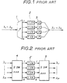
- FIG.1 shows a basic structure of the wavelength/time composite switch in an example of the conventional optical switching system.
- An optical input signal which is applied to a variable branching filter 1 is a wavelength-division multiplexed (wavelengths of ⁇ 1 through ⁇ n ) and time-division multiplexed signal.
- the variable branching filter 1 branches the input optical signal to k optical T switches 2 for every predetermined wavelength.
- the selecting wavelength of the variable branching filter 1 is switched for every time slot of the time-division multiplexed signal component.
- Outputs of the optical T switches 2 are converted into predetermined wavelengths for every time slot in variable wavelength converting elements 3.
- Outputs of the variable wavelength converting elements 3 are combined and output as an optical output signal of the wavelength/time composite switch.
- FIG.2 shows an equivalent circuit of the wavelength/time composite switch shown in FIG.1.
- n time division highways of the wavelengths ⁇ 1 through ⁇ n are coupled to k T switches 2' via an nxk S switch 4.
- Outputs of the T switches 2' are coupled to n time division highways of the wavelengths ⁇ 1 through ⁇ n via a kxn S switch 5.
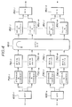
- FIG.3 shows a more detailed block diagram of the conventional optical switching system.
- a variable branching filter 1" branches a reference light in which a light having an accurate wavelength is wavelength-division multiplexed.
- the wavelength conversion is made by modulating outputs of the variable branching filter 1" in optically controlled optical modulators 3' depending on outputs of optical T switches 2".
- By switching the selecting wavelengths of the variable branching filter 1" for every time slot it is possible to also vary the wavelength for every time slot after the wavelength conversion.
- a wavelength synchronised switching network of essentially this form using wavelength switching, based on a variable wavelength filter and an optically controlled modulator is disclosed in IEEE INTERNATIONAL CONFERENCE ON COMMUNICATIONS - SOUND TO LIGHT, Seattle, Washington, 7-10 June 1987, vol. 3, pages 1565-1569 (Suzuki et al). This reference also discloses a ⁇ n switching network useful for constructing large-capacity switching systems.
- EP-A-0 264 119 discloses an optical wavelength-division switching system in which an electric signal is reproduced for each channel from a wavelength division multiplexed optical signal, and the electric signal is then used to modulate a light source (laser diode).
- the input optical signal which is a wavelength-division multiplexed and time-division multiplexed signal is conventionally subjected to the arbitrary interchange of the wavelength and the time slot in the above described manner.
- the conventional optical switching system is not practical in that it lacks flexibility in the interchange of information contents, collection of required information and the like, and a highly satisfactory service cannot be expected when applied to the information interchange services.
- an optical switching system comprising first means for receiving an input optical signal which is a wavelength-division multiplexed and time-division multiplexed signal, said first means including first separating means for separating and outputting a time-division multiplexed signal component of the input optical signal in each of divided wavelengths and second separating means for separating a control information included in the input optical signal, second means coupled to said first means for storing an optical signal output from said first means for every time slot identical to that used for the separation in said first means and for reading out stored optical signals successively in a sequence of predetermined time slots so as to convert wavelengths of the optical signals into predetermined wavelengths based on said control information, third means coupled to said second means for multiplexing wavelengths of optical signals output from said second means into wavelength-division multiplexed optical signals and for delaying a phase of the wavelength-division multiplexed optical signals a predetermined quantity, an optical data bus coupled to said third means for receiving optical signals output from said third means
- FIG.4 generally shows a first embodiment of an optical switching system according to the present invention.
- wavelength-division multiplexed signal separators 600-1 through 600-n each enter an input optical signal which is a wavelength-division multiplexed and time-division multiplexed signal and separate a time-division multiplexed signal component in each of the divided wavelengths.
- the wavelength-division multiplexed signal separators 600-1 through 600-n each read a control information included in the input optical signal and output an optical signal corresponding to the time-division multiplexed signal component.
- Optical storage and wavelength converters 730-1 through 730-m are coupled to each of the wavelength-division multiplexed signal separators 600-1 through 600-n and store optical signals output from the wavelength-division multiplexed signal separators 600-1 through 600-n for every time slot identical to that used for the separation in the wavelength-division multiplexed signal separators 600-1 through 600-n.
- the optical storage and wavelength converters 730-1 through 730-m read out the stored optical signals successively in a sequence of predetermined time slots and convert the wavelengths of the optical signals to predetermined wavelengths based on the control information.
- Optical multiplexer and delay parts 750-1 through 750-m each multiplex the wavelengths of an output optical signal of the corresponding one of the optical storage and wavelength converters 730-1 through 730-m and output the optical signal after delaying the phase of the optical signal a predetermined quantity.
- An optical bus 800 enters output optical signals of the optical multiplexer and delay parts 750-1 through 750-m and transfer these optical signals in a predetermined direction in an optical transmission path.
- the optical transmission path is a loop-shaped path.
- Optical delay and wavelength converters 850-1 through 850-m are coupled to the optical bus 800 and each extract an optical signal having wavelengths belonging to a predetermined wavelength region and delay the phase thereof a predetermined quantity so as to convert the wavelengths of the optical signal into predetermined wavelengths.
- Optical wavelength multiplexers 950-1 through 950-n are each coupled to the optical delay and wavelength converters 850-1 through 850-m and multiplex the wavelengths of the optical signal so as to output an optical output signal which is a wavelength-division multiplexed and time-division multiplexed signal.
- the output optical signal is obtained with a space multiplexing factor n, a wavelength multiplexing factor m and a time multiplexing factor m.
- the optical output signal of the optical switching system has a signal format approximately the same as that of the original optical input signal. In other words, the alignment of the optical wavelength, the center wavelength, the wavelength bandwidth and the like of the input optical signal and the output optical signal of the optical switching system are approximately the same.
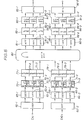
- FIG.5 shows the first embodiment in more detail.
- An optical input signal which is a wavelength-division multiplexed and time-division multiplexed signal is obtained from a plurality of channels.
- FIG.5 shows a case where there are two channels.
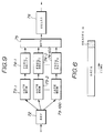
- the optical input signal is made up of cells having a fixed length and a header H as shown in FIG.6.
- the header H contains information such as a wavelength information ⁇ 1 of an optical input signal, a content information A 1 , a wavelength information ⁇ 2 of an optical output signal, an output channel information a 2 , an information quantity l 1 , a priority information ⁇ , and a time slot information t 2 , and may be described as H( ⁇ 1 , A 1 , ⁇ 2 , a 2 , l 1 , ⁇ , t 2 , ).
- the wavelength information ⁇ 2 includes ⁇ 21 , ⁇ 22 , ⁇ 23 , ... .
- the output channel information a 2 includes a 21 , a 22 , a 23 , ... , and may be used for making a broadcast.
- the time slot information t 2 includes t 21 , t 22 , t 23 , ... .
- the optical input signal received from a first channel CH1 is applied to an optical wavelength-division multiplexed signal separator (frequency divider) 60-1 wherein time-division multiplexed data are separated from the optical input signal in each of the divided wavelengths.
- Output optical signals of the optical wavelength-division multiplexed signal separator 60-1 are supplied to detectors 65-1 through 65-3 which detect a control information included in the optical signals. This control information is used to control time slot interchange and frequency shifters 70-1 through 70-3.
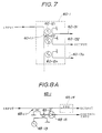
- the optical wavelength-division multiplexed signal separator 60-1 has a structure shown in FIG.7.
- Each ring optical resonator 60-12i is optically coupled to the optical fiber 60-11 and the corresponding optical fiber 60-13i.
- Each of the detectors 65-1 through 65-3 have a structure shown in FIG.8A, 8B or 8C.
- the detector 65-1 has optical couplers 65-11 and 65-12, an optical local oscillator 65-13, an optical delay circuit 65-14, and a photodetector 65-15.
- the optical signal from the optical wavelength-division multiplexed signal separator 60-1 is output via the optical delay circuit 65-14.
- the control information is extracted by the optical local oscillator 65-12 and is output from the photodetector 65-15 in the form of an electrical signal.
- the detector 65-1 has an optical coupler 65-21, an optical delay circuit 65-22, a photodetector 65-23, a local oscillator 65-24, and electrical tuners 65-251 through 65-25n.
- the optical signal from the optical wavelength-division multiplexed signal separator 60-1 is output via the optical coupler 65-21 and the optical delay circuit 65-14.
- a portion of the optical signal (for example, 1/10 the optical power) is branched by the optical coupler 65-21 and supplied to the photodetector 65-23.
- the electrical tuners 65-251 through 65-25n respectively detect the modulation frequency of the header of the optical signal responsive to an output of the local oscillator 65-24 and output control information CI 1 through CI n .
- the detector 65-1 has an optical coupler 65-31, an optical amplifier 65-32, an FM/AM converter 65-33, a photodetector 65-34, and electrical filters 65-351 through 54-35n having mutually different passbands.
- the optical signal from the optical wavelength-division multiplexed signal separator 60-1 is output via the optical coupler 65-31.
- the optical signal is branched by the optical coupler 65-31 and is supplied to the FM/AM converter 65-33 via the optical amplifier 65-32.
- a known semiconductor optical amplifier may be used as the optical amplifier 65-32.
- the FM/AM converter 65-33 comprises a known etalon element which passes an optical signal having a predetermined wavelength.
- FM frequency modulated
- AM amplitude modulated
- Output optical signals of the detectors 65-1 through 65-3 are supplied to the corresponding time slot interchange and frequency shifters 70-1 through 70-3.
- Each of the time slot interchange and frequency shifters 70-1 through 70-3 have a structure shown in FIG.9.
- the time slot interchange and frequency shifter comprises a time-division multiplexed signal separator 72, optical gate memories 73-1 through 73-100, optical frequency shifters 74-1 through 74-100, a wavelength multiplexer 75, and an optical delay circuit 76.
- the time-division multiplexed signal separator 72 separates 100 time-division multiplexed signals from the output optical signal of one of the detectors 65-1 through 65-3.
- An output optical signal or optical packet of the time-division multiplexed signal separator 72 is successively supplied and stored in the optical gate memories 73-1 through 73-100 in this sequence during mutually different time slots.
- the optical data stored in the optical gate memories 73-1 through 73-100 are read out based on the control information described above and supplied to the corresponding optical frequency shifters 74-1 through 74-100 which convert the wavelengths of the input optical signals into mutually different wavelengths.
- Output optical signals of the optical frequency shifters 74-1 through 74-100 are supplied to the wavelength multiplexer 75 wherein a wavelength multiplexing takes place.
- a wavelength-division multiplexed optical signal output from the wavelength multiplexer 75 is supplied to the optical delay circuit 76 which compensates for a phase error caused by different input positions of the optical signals to the optical bus 80.
- An output optical signal of the optical delay circuit 76 is supplied to the optical bus 80 via a corresponding one of optical couplers 77-1 through 77-3. Hence, the optical signal from the optical delay circuit 76 is transferred in a predetermined direction in the optical bus 80.
- the time-division multiplexed signal separator 72 has a structure shown in FIGS.10A and 10B.
- the time-division multiplexed signal separator 72 has an optical amplifier 721 and a star branch part 722.
- the optical amplifier 721 includes a semitransparent mirror 723 which receives a light for optical pumping, and Er doped fiber 724, and an optical filter 725.
- the time-division multiplexed signal separator 72 has optical fibers 725 and electrodes 726 provided on a chip 727.
- the output optical signal of the time-division multiplexed signal separator 72 is controlled responsive to a control signal applied to the electrodes 726.
- a known optical memory may be used for the optical gate memories 73-1 through 73-100.
- Each of the optical couplers 77-1 through 77-3 have a structure shown in FIG.11.
- the optical coupler 77-1 has an optical fiber 77-10 which is optically coupled to the optical data bus 80 at a portion 77-11.
- One end of the optical fiber 77-10 is connected to an absorbing part 77-12 which absorbs the optical signal transferred within the optical fiber 77-10.
- a known optical frequency shifter may be used for the optical frequency shifters 74-1 through 74-100.
- a wavelength conversion element proposed in Kuno et al. "Study on the Wavelength-Switching Devices Using Bistable DFB Lasers", National Conference of Semiconductor/Materials Group of Electronics and Information Communication Society, 1987 or a wavelength conversion element proposed in Kondo et al., "A Tunable Optical-Wavelength Conversion Laser with TM-Polarized Light Input", National Conference of Electronics and Information Communication Society, Fall 1988.
- optically coupled bandpass filters 81-1 through 81-3 each output an optical signal which is obtained from the optical bus 80 and has a wavelength in a vicinity of a center wavelength thereof, that is, a wavelength within a predetermined wavelength range.
- Optical signals output from the optically coupled bandpass filters 81-1 through 81-3 are supplied to corresponding optical delay circuits 85-1 through 85-3 wherein a phase error compensation similar to that described above takes place.
- a known optical delay element may be used for the optical delay circuits 85-1 through 85-3.
- Optical signals output from the optical delay circuits 85-1 through 85-3 are supplied to corresponding optical frequency shifters 90-1 through 90-3 wherein the wavelengths of the optical signals are returned to the original wavelengths.
- Optical signals output from the optical frequency shifters 90-1 through 90-3 are supplied to a wavelength multiplexer 95-1 which multiplexes the wavelengths of the optical signals, and an output optical signal of the wavelength multiplexer 95-1 is transferred to an optical fiber (not shown), for example.
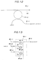
- Each of the optically coupled bandpass filters 81-1 through 81-3 have a structure shown in FIG.12.
- the optically coupled bandpass filter 81-1 has a ring optical resonator 81-10 and an optical fiber 81-11.
- the ring optical resonator 81-10 is optically coupled to the optical data bus 80 and the optical fiber 81-11.
- the optical fiber 81-11 transfers the passed optical signal to the corresponding optical delay circuit 81-1.
- the wavelength multiplexer 95-1 has a construction shown in FIG.13.
- Each optical resonator 95-2i is optically coupled to the corresponding optical fiber 95-1i and the optical fiber 95-3.
- the optical input signal received from a second channel CH2 is processed similarly to the optical input signal received from the first channel CH1. For this reason, a description of an optical wavelength-division multiplexed signal separator 60-2, detectors 66-1 through 66-3, time slot interchange and frequency shifters 71-1 through 71-3, optical couplers 78-1 through 78-3, optically coupled bandpass filters 82-1 through 82-3, optical delay circuits 86-1 through 86-3, optical frequency shifters 91-1 through 91-3, and a wavelength multiplexer 95-2 will be omitted.
- FIGS.14A and 14B respectively show the input optical signal and the output optical signal of the first embodiment.
- signals S1, S2 and S3 are time-division multiplexed to a wavelength ⁇ 1 of the input optical signal
- signals S1', S2' and S3' are time-division multiplexed to a wavelength ⁇ 2 of the input optical signal
- signals S1", S2" and S3" are time-division multiplexed to a wavelength ⁇ 3 of the input optical signal.
- signals S2, S1' and S3' are time-division multiplexed to the wavelength ⁇ 1 of the input optical signal
- signals S1', S2" are time-division multiplexed to the wavelength ⁇ 2 of the input optical signal
- signals S1", S2' and S3 are time-division multiplexed to the wavelength ⁇ 3 of the input optical signal.
- the optical output signal of the optical switching system has the same multiplexing factor (a, b, c).
- the b optical frequencies from the optical wavelength-division multiplexed signal separator 60-1 are supplied to the corresponding b detectors 65-1 through 65-b wherein a routing information is extracted.
- the routing information includes the number a of output optical fibers of the optical switching system, the number b of optical frequencies output from the optical switching system and a time-division slot address (time slot number) c at the time of output.
- the optical signals stored in the optical gate memories 73-1 through 73-c may be read out at the same time, but no problems are introduced thereby. This is because the optical frequencies of the optical signal are all converted in the c optical frequency shifters 74-1 through 74-c shown in FIG.9 so as to carry out a routing in conformance with the extracted routing information.
- the optical frequency shifters 74-1 through 74-c are optical frequency converters.
- a subscript "112" is adjacent to the 111th optical frequency and only the value of c differs by "1". In other words, the number of optical fibers and the optical frequencies at the time of output are the same as those at the time of input, but the time slot number c increases by "1".
- the routing information is included in a portion of the header H shown in FIG.6.
- the header H includes the routing information of the above Table 1.
- the header H additionally includes an information instructing a broadcasting of the same information, a priority of the information, the size (length) of the information and the like.
- the optical gate memory 73-1 for example is not only opened during one time slot but is opened during a number of time slots to send the information a plurality of times to output a plurality of optical signals (a', b', c'), (a", b", c"), (a, b, c), ... .
- the same information is transferred for the number a' of optical fibers, the number b' of optical frequencies and the time slot number c.
- the information having a high priority it is for example possible to give priority to the information over other information by assigning a small number to a portion of the number "abc".
- the optical data bus has the loop shape. However, it is not essential that the optical data bus has the loop shape.
- the rules of frequency conversion are as follows.
- an optical packet routing information within the header H is denoted by (a, b, c), and it is assumed that an optical packet signal having a frequency X is converted into an optical packet signal having a frequency "abc".
- a denotes a number of output optical fibers (number of output highways)
- b denotes an output optical frequency (output highway freqency)
- c denotes an output time slot (output highway time slot).
- the optical frequencies of all the optical packet signals are converted depending on the optical packet routing information (a, b, c), and the converted optical frequencies are sequentially arranged depending on the values of "abc" as shown in the following Table 2.
- This Table 2 shows the optical packet arrangement in the optical data bus.
- the same output highway signals packets
- the group is named the a-group as shown in the Table 2.
- the packets of the same output highway frequency have the same first two digits as "ab#" and this group is named the b-group.
Landscapes
- Engineering & Computer Science (AREA)
- Computer Networks & Wireless Communication (AREA)
- Optical Communication System (AREA)
- Use Of Switch Circuits For Exchanges And Methods Of Control Of Multiplex Exchanges (AREA)
Claims (13)
- Système de commutation optique comportant :
des premiers moyens (600-1 - 600-n) pour recevoir un signal optique d'entrée qui est un signal multiplexé par division de longueur d'onde et multiplexé temporellement, lesdits premiers moyens comprenant des premiers moyens de séparation pour séparer et délivrer une composante de signal multiplexée temporellement du signal optique d'entrée en chacune des longueurs d'onde divisées et des seconds moyens de séparation pour séparer une information de contrôle comprise dans le signal optique d'entrée; des seconds moyens (730-1 - 730-m) couplés auxdits premiers moyens pour mémoriser un signal optique délivré par lesdits premiers moyens pour chaque secteur de temps identique à celui utilisé pour la séparation dans lesdits premiers moyens et pour lire des signaux optiques mémorisés successivement dans une succession de secteurs de temps prédéterminés de manière à convertir des longueurs d'onde de signaux optiques en longueurs d'onde prédéterminée en fonction de ladite information de contrôle; des troisièmes moyens (750-1 - 750-m) couplés auxdits seconds moyens pour multiplexer les longueurs d'onde de signaux optiques délivrés par lesdits seconds moyens en signaux optiques multiplexés par division de longueur d'onde et pour retarder la phase des signaux optiques multiplexés par division de longueur d'onde d'une certaine quantité; un bus de données optiques (800) couplé auxdits troisièmes moyens pour recevoir des signaux optiques délivrés par lesdits troisièmes moyens et pour transférer les signaux optiques dans une direction prédéterminée à l'intérieur dudit bus de données optiques; des quatrièmes moyens (850-1 - 850-m) couplés audit bus de données optiques pour extraire des signaux optiques ayant des longueurs d'onde appartenant à des gammes de longueurs d'onde prédéterminées dudit bus de données optiques et retarder la phase des signaux optiques extraits d'une quantité prédéterminée et pour convertir les longueurs d'onde des signaux optiques extraits en longueurs d'onde prédéterminées; et des cinquièmes moyens (950-1 - 950-n) couplés auxdits quatrièmes moyens pour multiplexer les longueurs d'onde des signaux optiques délivrés par lesdits quatrièmes moyens de manière à délivrer un signal optique de sortie qui est un signal multiplexé par division de longueur d'onde et multiplexé temporellement. - Système de commutation optique selon la revendication 1, caractérisé en ce que lesdits premiers moyens de séparation desdits premiers moyens (600-1 - 600-n) comportent un diviseur de fréquence (60-1, 60-2) et des seconds moyens de séparation desdits premiers moyens comportent un détecteur (65-1 - 65-3, 66-1 - 66-3) pour détecter l'information de contrôle comprise dans le signal optique d'entrée et pour délivrer le signal optique d'entrée.
- Système de commutation optique selon la revendication 1 ou 2, caractérisé en ce que lesdits seconds moyens (730-1 - 730-m) comportent pour chaque signal optique délivré par lesdits premiers moyens (600-1 - 600-n) un séparateur de signaux multiplexés temporellement (72) pour séparer des signaux optiques multiplexés temporellement du signal optique délivré par lesdits premiers moyens, des mémoires optiques (73-1 - 73-100) pour mémoriser les signaux optiques multiplexés temporellement ou le signal de sortie de paquet optique provenant dudit séparateur de signaux multiplexés temporellement durant des secteurs de temps mutuellement différents, et un décaleur de fréquence (74-1 - 74-100) pour convertir en longueurs d'onde prédéterminées les longueurs d'onde des signaux optiques qui sont lus desdites mémoires optiques en fonction de ladite information de contrôle.
- Système de commutation optique selon l'une quelconque des revendications 1 à 3, caractérisé en ce que lesdits troisièmes moyens (750-1 - 750-m) comportent un multiplexeur de longueurs d'onde (75) pour multiplexer les signaux optiques délivrés par lesdits seconds moyens (730-1 - 730-m) en un signal optique multiplexé par division de longueur d'onde, et un circuit de retard optique (76) pour retarder d'une quantité prédéterminée la phase du signal optique multiplexé par division de longueurs d'onde.
- Système de commutation optique selon la revendication 4, caractérisé en ce que lesdits troisièmes moyens (750-1 - 750-m) comportent, en outre, pour chaque signal optique multiplexé par division de longueur d'onde délivré par ledit circuit de retard optique (76), un coupleur optique (77-1 - 77-3, 78-1 - 78-3) pour coupler optiquement ledit circuit de retard optique audit bus de données optiques (800).
- Système de commutation optique selon l'une quelconque des revendications 1 à 5, caractérisé en ce que ledit bus de données optiques (800) comporte une fibre optique en forme de boucle.
- Système de commutation optique selon l'une quelconque des revendications 1 à 6, caractérisé en ce que lesdits quatrièmes moyens (850-1 - 850-m) comportent un filtre passe-bande optique (81-1 - 81-3, 82-1 - 82-3) pour extraire les signaux optiques ayant les longueurs d'onde appartenant aux gammes de longueur d'onde prédéterminées dudit bus de données optiques (800).
- Système de commutation optique selon la revendication 7, caractérisé en ce que lesdits quatrièmes moyens (850-1 - 850-m) comportent, en outre, un circuit de retard optique (85-1 - 85-3, 86-1 - 86-3) pour retarder d'une quantité prédéterminée la phase des signaux optiques extraits, et un décaleur de fréquence (90-1 - 90-3, 91-1 - 91-3) pour convertir les longueurs d'onde des signaux optiques extraits dudit circuit de retard optique en longueurs d'onde prédéterminées.
- Système de commutation optique selon l'une quelconques des revendications 1 à 8, caractérisé en ce que ladite information de contrôle contient au moins une information choisie parmi un groupe comprenant une information de longueur d'onde du signal d'entrée optique, une information de contenu, une information de longueur d'onde du signal de sortie optique, une information de canal de sortie, une quantité d'information, une information de priorité, et une information de secteur de temps.
- Système de commutation optique selon l'une quelconque des revendications 1 à 9, caractérisé en ce que ledit signal optique d'entrée est constitué de cellules ayant une longueur fixe et un en-tête qui comprend une information d'acheminement, ladite information d'acheminement comprenant une pluralité a de fibres optiques de sortie qui sont couplées à un côté sortie desdits cinquièmes moyens, une fréquence optique b et un secteur de temps de sortie c.
- Système de commutation optique selon la revendication 10, caractérisé en ce que lesdits seconds moyens (730-1 - 730-m) sont disposés pour convertir les longueurs d'onde de tous les signaux optiques mémorisés en fonction de valeurs de l'information d'acheminement (a, b, c).
- Système de commutation optique selon la revendication 11, caractérisé en ce que lesdits seconds moyens (730-1 - 730-m) sont disposés pour convertir les fréquences optiques de tous les signaux optiques mémorisés en longueurs d'onde prédéterminées en fonction de l'information de contrôle.
- Système de commutation optique selon l'une quelconque des revendications 1 à 12, caractérisé en ce que lesdits premiers à cinquièmes moyens sont disposés pour traiter des signaux optiques par un traitement entièrement optique.
Priority Applications (1)
| Application Number | Priority Date | Filing Date | Title |
|---|---|---|---|
| EP96109491A EP0741498A3 (fr) | 1988-07-18 | 1989-07-14 | Système de communication optique |
Applications Claiming Priority (2)
| Application Number | Priority Date | Filing Date | Title |
|---|---|---|---|
| JP63178512A JPH0712230B2 (ja) | 1988-07-18 | 1988-07-18 | 光交換システム |
| JP178512/88 | 1988-07-18 |
Related Child Applications (1)
| Application Number | Title | Priority Date | Filing Date |
|---|---|---|---|
| EP96109491.9 Division-Into | 1989-07-14 |
Publications (3)
| Publication Number | Publication Date |
|---|---|
| EP0351729A2 EP0351729A2 (fr) | 1990-01-24 |
| EP0351729A3 EP0351729A3 (fr) | 1992-01-15 |
| EP0351729B1 true EP0351729B1 (fr) | 1997-01-29 |
Family
ID=16049770
Family Applications (2)
| Application Number | Title | Priority Date | Filing Date |
|---|---|---|---|
| EP89112944A Expired - Lifetime EP0351729B1 (fr) | 1988-07-18 | 1989-07-14 | Système de communication optique |
| EP96109491A Withdrawn EP0741498A3 (fr) | 1988-07-18 | 1989-07-14 | Système de communication optique |
Family Applications After (1)
| Application Number | Title | Priority Date | Filing Date |
|---|---|---|---|
| EP96109491A Withdrawn EP0741498A3 (fr) | 1988-07-18 | 1989-07-14 | Système de communication optique |
Country Status (5)
| Country | Link |
|---|---|
| US (1) | US5023863A (fr) |
| EP (2) | EP0351729B1 (fr) |
| JP (1) | JPH0712230B2 (fr) |
| CA (1) | CA1313319C (fr) |
| DE (1) | DE68927724T2 (fr) |
Families Citing this family (29)
| Publication number | Priority date | Publication date | Assignee | Title |
|---|---|---|---|---|
| IT1233075B (it) * | 1989-08-01 | 1992-03-14 | Cselt Centro Studi Lab Telecom | Commutatore veloce di pacchetto e frequenza |
| US5105292A (en) * | 1989-10-02 | 1992-04-14 | Alcatel Cit | Asynchronous optical communication system |
| FR2660500B2 (fr) * | 1990-03-29 | 1994-04-22 | Cit Alcatel | Systeme de communication optique temporel asynchrone. |
| FR2672175A1 (fr) * | 1991-01-29 | 1992-07-31 | Cit Alcatel | Centre satellite photonique. |
| FR2672172B1 (fr) * | 1991-01-29 | 1993-06-04 | Cit Alcatel | Matrice de commutation photonique. |
| FR2672178B1 (fr) * | 1991-01-29 | 1994-03-18 | Alcatel Cit | Concentrateur photonique. |
| GB9106181D0 (en) * | 1991-03-22 | 1991-05-08 | British Telecomm | Photonic amplifier |
| IT1255810B (it) * | 1992-08-07 | 1995-11-16 | Alcatel Italia | Rete di connessione fotonica a commutazione di pacchetto per la diffusione d'informazioni |
| GB9220592D0 (en) * | 1992-09-30 | 1992-11-11 | Plessey Telecomm | Optic switching |
| US5495356A (en) * | 1993-04-30 | 1996-02-27 | Nec Research Institute, Inc. | Multidimensional switching networks |
| DE69434263T2 (de) * | 1993-07-14 | 2006-01-12 | Nippon Telegraph And Telephone Corp. | Photonisches Koppelfeld mit Frequenzweglenkung für Zeitmultiplexstrecken |
| EP0639037B1 (fr) * | 1993-07-14 | 2002-10-02 | Nippon Telegraph And Telephone Corporation | Tampon PEPS photonique avec multiplexage en fréquence |
| GB2282018B (en) * | 1993-09-14 | 1998-03-18 | Northern Telecom Ltd | Optical communications network |
| FR2725528B1 (fr) * | 1994-10-11 | 1996-11-22 | Alcatel Nv | Ligne a retard optique selectif en longueur d'onde |
| US5490007A (en) * | 1994-10-31 | 1996-02-06 | Hewlett-Packard Company | Bypass switching and messaging mechanism for providing intermix data transfer for a fiber optic switch |
| FR2754352B1 (fr) * | 1996-10-07 | 1998-11-13 | Alsthom Cge Alcatel | Commutateur optique |
| JPH11275614A (ja) | 1998-03-26 | 1999-10-08 | Nec Corp | 光交換装置 |
| US20010046348A1 (en) * | 2000-04-20 | 2001-11-29 | Stig Sarkimukka | Multi-wavelength/multi-channel system |
| US20020126347A1 (en) * | 2001-03-07 | 2002-09-12 | Hogan Josh N. | High data rate multiple wavelength encoding |
| JP4160907B2 (ja) * | 2002-01-30 | 2008-10-08 | エリクソン テレコムニカコエス エス.アー | 周波数ヘッダを使用する光パケットスイッチングのための装置、システムと方法 |
| US7809278B2 (en) | 2004-07-26 | 2010-10-05 | Hewlett-Packard Development Company, L.P. | Apparatus and method of providing separate control and data channels between arrays of light emitters and detectors for optical communication and alignment |
| US7623783B2 (en) | 2004-08-10 | 2009-11-24 | Hewlett-Packard Development Company, L.P. | System and method of self-configuring optical communication channels between arrays of emitters and detectors |
| US7269321B2 (en) | 2004-08-10 | 2007-09-11 | Hewlett-Packard Development Company, L.P. | System and method of configuring fiber optic communication channels between arrays of emitters and detectors |
| US7623793B2 (en) | 2004-08-10 | 2009-11-24 | Hewlett-Packard Development Company, L.P. | System and method of configuring fiber optic communication channels between arrays of emitters and detectors |
| US7251388B2 (en) | 2004-08-10 | 2007-07-31 | Hewlett-Packard Development Company, L.P. | Apparatus for providing optical communication between integrated circuits of different PC boards and an integrated circuit assembly for use therein |
| US7653108B2 (en) | 2004-09-09 | 2010-01-26 | Hewlett-Packard Development Company, L.P. | Apparatus and method of establishing optical communication channels between a steerable array of laser emitters and an array of optical detectors |
| US7229218B2 (en) | 2004-09-20 | 2007-06-12 | Hewlett-Packard Development Company, L.P. | Apparatus and method of providing an optical connection between PC boards for optical communication |
| US7987066B2 (en) * | 2008-08-29 | 2011-07-26 | Bae Systems Information And Electronic Systems Integration Inc. | Components and configurations for test and valuation of integrated optical busses |
| EP3432494B1 (fr) * | 2017-07-17 | 2021-09-08 | ADVA Optical Networking SE | Procédé et appareil pour permettre un seul usinage de fibre sur une fibre optique |
Family Cites Families (13)
| Publication number | Priority date | Publication date | Assignee | Title |
|---|---|---|---|---|
| JPS5866487A (ja) * | 1981-10-16 | 1983-04-20 | Fujitsu Ltd | 光ハイウェイスイッチ |
| JPS59158661A (ja) * | 1983-03-01 | 1984-09-08 | Nec Corp | 光交換器 |
| DE3484345D1 (de) * | 1983-07-08 | 1991-05-02 | American Telephone & Telegraph | Optische uebertragungssysteme mit multiplexierung durch wellenlaengenabspaltung. |
| JPS6196893A (ja) * | 1984-10-18 | 1986-05-15 | Fujitsu Ltd | 複合型光交換装置 |
| JPS61184997A (ja) * | 1985-02-12 | 1986-08-18 | Nec Corp | 光時間スイツチ |
| JPH0681119B2 (ja) * | 1986-04-17 | 1994-10-12 | 日本電気株式会社 | 波長多重光伝送方式 |
| GB2191645B (en) * | 1986-06-13 | 1990-09-05 | Stc Plc | Optical telecommunication systems |
| JPH0714228B2 (ja) * | 1986-08-20 | 1995-02-15 | 富士通株式会社 | 時分割波長分割併合型光交換通話路装置 |
| JPH0636621B2 (ja) * | 1986-10-15 | 1994-05-11 | 日本電気株式会社 | 光交換機 |
| JP2527553B2 (ja) * | 1987-03-10 | 1996-08-28 | 富士通株式会社 | 光多元交換装置 |
| JPS6411493A (en) * | 1987-07-03 | 1989-01-17 | Fujitsu Ltd | Time division optical exchanging device using wavelength division multiplex |
| JP2688352B2 (ja) * | 1987-08-10 | 1997-12-10 | 日本電信電話株式会社 | 光通信方式およびシステム |
| JPS6490696A (en) * | 1987-09-30 | 1989-04-07 | Nec Corp | Wavelength/time division optical exchange |
-
1988
- 1988-07-18 JP JP63178512A patent/JPH0712230B2/ja not_active Expired - Lifetime
-
1989
- 1989-07-14 DE DE68927724T patent/DE68927724T2/de not_active Expired - Fee Related
- 1989-07-14 EP EP89112944A patent/EP0351729B1/fr not_active Expired - Lifetime
- 1989-07-14 EP EP96109491A patent/EP0741498A3/fr not_active Withdrawn
- 1989-07-17 CA CA000605871A patent/CA1313319C/fr not_active Expired - Fee Related
- 1989-07-18 US US07/381,595 patent/US5023863A/en not_active Expired - Fee Related
Also Published As
| Publication number | Publication date |
|---|---|
| EP0741498A3 (fr) | 1997-05-28 |
| EP0351729A2 (fr) | 1990-01-24 |
| EP0351729A3 (fr) | 1992-01-15 |
| JPH0227892A (ja) | 1990-01-30 |
| DE68927724T2 (de) | 1997-06-05 |
| DE68927724D1 (de) | 1997-03-13 |
| JPH0712230B2 (ja) | 1995-02-08 |
| EP0741498A2 (fr) | 1996-11-06 |
| US5023863A (en) | 1991-06-11 |
| CA1313319C (fr) | 1993-02-02 |
Similar Documents
| Publication | Publication Date | Title |
|---|---|---|
| US5023863A (en) | Optical switching system | |
| JP2989269B2 (ja) | 光ネットワーク用交差接続 | |
| KR0142177B1 (ko) | 광 스위치 및 그 스위칭 모듈 | |
| Tucker et al. | Photonic packet switching: An overview | |
| US4821255A (en) | Cross-connection of wavelength-division-multiplexed high speed optical channels | |
| US7106967B2 (en) | Optical packet switching apparatus and methods | |
| EP0639015B1 (fr) | Commutateur pour une voie photonique à division temporelle avec routage en fréquence | |
| EP1353526B1 (fr) | Commutateur optique à haute vitesse | |
| CA2044669C (fr) | Commutateur optique | |
| KR100237838B1 (ko) | 대용량 광비동기전송 모드스위치 | |
| EP0726691A2 (fr) | Routeur de longueur d'onde combiné avec un commutateur pour un système de communication optique par multiplexage en longueur d'onde | |
| JPH0636621B2 (ja) | 光交換機 | |
| US6252698B1 (en) | Method and device for wavelength conversion, and system including the device | |
| EP0410096B1 (fr) | Commutateur photonique à répartition en longueurs d'ondes | |
| AU657606B2 (en) | Multistage switching facility for optical signals | |
| US5121381A (en) | Optical switching apparatus for digital signal cross connection and method of interswitch optical transmission of digital signals | |
| Gambini | State of the art of photonic packet switched networks | |
| US6643042B1 (en) | Optical communication network node | |
| JPH06121357A (ja) | 光スイッチ回路 | |
| EP0571132A1 (fr) | Récepteur optique accordable | |
| JP2924887B1 (ja) | 光通信ネットワークノード | |
| Gabriagues et al. | Design Implementation of a Gigabit ATM Photonic Switching Matrix | |
| JP2920790B2 (ja) | パケットスイッチ | |
| Gabriagues et al. | Design, modelling and implementation of the ATMOS project fibre delay line photonic switching matrix | |
| JP3069207B2 (ja) | 光atm通話路 |
Legal Events
| Date | Code | Title | Description |
|---|---|---|---|
| PUAI | Public reference made under article 153(3) epc to a published international application that has entered the european phase |
Free format text: ORIGINAL CODE: 0009012 |
|
| AK | Designated contracting states |
Kind code of ref document: A2 Designated state(s): DE FR GB |
|
| PUAL | Search report despatched |
Free format text: ORIGINAL CODE: 0009013 |
|
| AK | Designated contracting states |
Kind code of ref document: A3 Designated state(s): DE FR GB |
|
| 17P | Request for examination filed |
Effective date: 19920211 |
|
| 17Q | First examination report despatched |
Effective date: 19940325 |
|
| GRAG | Despatch of communication of intention to grant |
Free format text: ORIGINAL CODE: EPIDOS AGRA |
|
| GRAH | Despatch of communication of intention to grant a patent |
Free format text: ORIGINAL CODE: EPIDOS IGRA |
|
| GRAH | Despatch of communication of intention to grant a patent |
Free format text: ORIGINAL CODE: EPIDOS IGRA |
|
| GRAA | (expected) grant |
Free format text: ORIGINAL CODE: 0009210 |
|
| AK | Designated contracting states |
Kind code of ref document: B1 Designated state(s): DE FR GB |
|
| XX | Miscellaneous (additional remarks) |
Free format text: TEILANMELDUNG 96109491.9 EINGEREICHT AM 13/06/96. |
|
| REF | Corresponds to: |
Ref document number: 68927724 Country of ref document: DE Date of ref document: 19970313 |
|
| ET | Fr: translation filed | ||
| PLBE | No opposition filed within time limit |
Free format text: ORIGINAL CODE: 0009261 |
|
| STAA | Information on the status of an ep patent application or granted ep patent |
Free format text: STATUS: NO OPPOSITION FILED WITHIN TIME LIMIT |
|
| 26N | No opposition filed | ||
| PGFP | Annual fee paid to national office [announced via postgrant information from national office to epo] |
Ref country code: FR Payment date: 19990709 Year of fee payment: 11 |
|
| PGFP | Annual fee paid to national office [announced via postgrant information from national office to epo] |
Ref country code: GB Payment date: 19990714 Year of fee payment: 11 |
|
| PGFP | Annual fee paid to national office [announced via postgrant information from national office to epo] |
Ref country code: DE Payment date: 19990716 Year of fee payment: 11 |
|
| PG25 | Lapsed in a contracting state [announced via postgrant information from national office to epo] |
Ref country code: GB Free format text: LAPSE BECAUSE OF NON-PAYMENT OF DUE FEES Effective date: 20000714 |
|
| GBPC | Gb: european patent ceased through non-payment of renewal fee |
Effective date: 20000714 |
|
| PG25 | Lapsed in a contracting state [announced via postgrant information from national office to epo] |
Ref country code: FR Free format text: LAPSE BECAUSE OF NON-PAYMENT OF DUE FEES Effective date: 20010330 |
|
| REG | Reference to a national code |
Ref country code: FR Ref legal event code: ST |
|
| PG25 | Lapsed in a contracting state [announced via postgrant information from national office to epo] |
Ref country code: DE Free format text: LAPSE BECAUSE OF NON-PAYMENT OF DUE FEES Effective date: 20010501 |