EP0351984A2 - Interface programmable pour carte de circuit périphérique de système d'ordinateur - Google Patents
Interface programmable pour carte de circuit périphérique de système d'ordinateur Download PDFInfo
- Publication number
- EP0351984A2 EP0351984A2 EP89306840A EP89306840A EP0351984A2 EP 0351984 A2 EP0351984 A2 EP 0351984A2 EP 89306840 A EP89306840 A EP 89306840A EP 89306840 A EP89306840 A EP 89306840A EP 0351984 A2 EP0351984 A2 EP 0351984A2
- Authority
- EP
- European Patent Office
- Prior art keywords
- programmable
- interface
- address
- peripheral circuit
- circuit card
- Prior art date
- Legal status (The legal status is an assumption and is not a legal conclusion. Google has not performed a legal analysis and makes no representation as to the accuracy of the status listed.)
- Granted
Links
Images


Classifications
-
- G—PHYSICS
- G06—COMPUTING OR CALCULATING; COUNTING
- G06F—ELECTRIC DIGITAL DATA PROCESSING
- G06F12/00—Accessing, addressing or allocating within memory systems or architectures
- G06F12/02—Addressing or allocation; Relocation
- G06F12/06—Addressing a physical block of locations, e.g. base addressing, module addressing, memory dedication
- G06F12/0646—Configuration or reconfiguration
- G06F12/0653—Configuration or reconfiguration with centralised address assignment
- G06F12/0661—Configuration or reconfiguration with centralised address assignment and decentralised selection
Definitions
- This invention relates to a programmable interface for peripheral circuit cards in computer systems, particularly personal computer systems. More particularly, this invention relates to such an interface using special-purpose programmable logic devices to enable a designer of peripheral circuit cards to customize the interface to the computer bus for a particular card design.
- Computer systems typically include (a) a central processor unit which, in the case of a personal computer, is a microprocessor; (b) a main circuit board, including the central processor unit, memory devices and other essential circuits; (c) mass storage devices such as disk drives and associated controller circuits; (d) one or more ports for communication with peripheral devices; and, optionally, (e) one or more printed circuit cards for performing various optional functions, such as additional memory, graphics, communication or storage resources and control. These printed circuit cards will hereafter be referred to as "peripheral circuit cards".
- the central processor unit, memory devices, mass storage devices, ports and peripheral circuit cards all communicate with one another over a communications bus under a particular protocol defined by the bus architecture.
- This communications bus is termed the system bus.
- This system bus typically will include address, data, control and arbitration control lines.
- the arbitration control lines allow devices other than the central processor unit to gain control of the bus. In this manner, these devices, termed bus masters, may control the transfer of data across the bus.
- the central processor unit or other bus master can transfer data from one device or card to another as needed, e.g., from mass storage device to main memory.
- each device must have a unique address to allow the unique selection of data sources and destinations. Bus conflicts result if addresses are not unique -- e.g., two or more devices attempting to transfer data to or from the bus at once.
- a representative bus is described in "Micro Channel® Architecture Specification” and “IBM® Personal System/2® Seminar Proceedings”, both available from International Business Machines Corporation.
- a peripheral circuit card To interface to the described bus, a peripheral circuit card must:
- system bus is used to initialize the peripheral circuit cards when the system is powered up. This initialization includes the assignment of unique, conflict-free addresses to each card and the configuration of specific card functions.
- each peripheral circuit card designed for this bus must have a 16-bit card identification number which is readable by the central processor unit.
- This card identification number is unique to a particular peripheral card design. It must be stored on the card in a non-volatile manner; that is, when system power is removed, the identication number must be retained for use on subsequent system power-up.
- the central processor unit reads the card identification number for each peripheral circuit card present. It then reads a configuration file stored on the system disk drive associated with the peripheral circuit card identification number detected.
- the configuration file includes a list of alternative addresses by which the peripheral circuit card can be addressed.
- the configuration file also specifies data patterns to be written into special configuration registers on the peripheral circuit card to enable each of the available address ranges.
- the central processor unit can therefore control the addresses to which each peripheral circuit card responds by writing the appropriate values into the configuration registers. By this means, the central processor unit can eliminate address conflicts between peripheral circuit cards by choosing appropriate, non-conflicting addresses for each card during initialization.
- the configuration registers may also be used as software-controlled ports to control specific functions on the peripheral circuit card.
- the central processor unit may control specific system hardware functions.
- Two of the bits in these registers are specified in the bus specification.
- One of these bits acts as a peripheral circuit card enable bit -- i.e., until this bit is written to a logical "1" by the central processor unit, the peripheral circuit card will remain inactive.
- Another of these bits acts as a non-maskable interrupt flag, which can be written by the central processor unit with a logical "0" to clear an interrupt condition.
- Remaining bits in the four 8-bit configuration registers can be used for address selection as described above, or for whatever configuration functions are deemed necessary by the card designer. A given card design will not generally require the use of all remaining register bits, and different card designs may in fact require different sets of register bits.
- peripheral card identification chip select address decode ranges
- latching of chip selects chip select/feedback "OR”ing
- register bit patterns which enable address range selections, and register/pin connections programmable in a non-volatile fashion.
- Non-volatile programming of these features would allow the programmable interface to retain the particular characteristics required in a given peripheral circuit card design even when power is removed from the peripheral circuit card and the associated computer system.
- Non-volatile programming of these features allows the programmable interface to retain the particular characteristics required in a given peripheral circuit card design even when power is removed from the peripheral circuit card and the associated computer system.
- a programmable interface for use between a communications bus in a computer system and a peripheral circuit card in the computer system.
- the peripheral circuit card has configuration registers for indicating to the computer system via the data communications bus various characteristics of the peripheral circuit card.
- the peripheral circuit card further has at least one application circuit chip thereon. The characteristics in the configuration registers include an address for the at least one chip.
- the programmable interface includes address input means for supplying to the interface address signals from the communications bus, programmable mask means for storing at least one address range for each of the at least one application circuit chip, comparator means associated with the mask means, means for applying the address signals to the comparator means, and means for generating an enable signal to enable the at least one chip when the address signals match the mask.
- the peripheral circuit card can be assembled using the at least one application circuit chip and the programmable interface, without the use of a custom interface.
- EPROM erasable programmable read-only memory
- EEPROM electrically-erasable programmable read-only memory
- Flash EPROM Flash EPROM
- the peripheral circuit card identification number is held in programmable, read-only registers for indicating to the computer system via the system bus the card type. In conjunction with data stored on the system disk, various characteristics of the peripheral circuit card may be ascertained by the system.
- the card furthermore has certain read/write configuration registers which can be used to control the address response ranges of the integrated circuits on the card as well as other card-specific hardware configuration selections.
- the programmable interface also includes programmable interconnect means to allow connection of configuration register bits with general-purpose input/output pins. In this manner, any desired bits from the configuration registers may selectively be brought out to interface pins for control of peripheral circuit card functions. Alternatively, peripheral circuit card logic may drive the input/output pins to provide status reporting to the central processor unit when the configuration register data is read.
- the peripheral circuit card can be assembled using the at least one application circuit chip and the programmable interface without the use of a custom interface.
- the present invention provides a generic programmable interface for the bus described above.
- a designer of peripheral circuit cards for use in a computer system having that bus need not have a custom interface made in order to develop the peripheral circuit card.
- the peripheral circuit card can be designed using interface chips according to the present invention, programmed by the designer. Once the interface design is finalized along with the rest of the peripheral circuit card, the designer may elect to have a custom interface chip made at that time.
- the peripheral circuit card is not expected to be manufactured in large quantities, it may be advantageous to use the programmable interface according to the invention even in production versions of the peripheral circuit card.
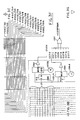
- FIGS. 1-5 represent a preferred embodiment of the programmable interface function of this invention, which provides a programmable interface between a peripheral circuit card and the bus referred to above.
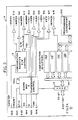
- FIG. 1 shows the programmable interface device as incorporated into a typical peripheral circuit card interface to the described bus.
- the programmable interface device 10 provides the primary address, control signal and configuration interface between the bus and any integrated circuit application chips on the peripheral circuit card.
- Data transceiver components 60 controlled by the programmable interface 10, provide a data transfer path between the the application chips on the peripheral circuit card and the D0-D15 bus data lines 400-415.
- One, two or four transceiver components 60 may be used depending on whether the peripheral circuit card has an 8-, 16- or 32-bit buffered board data bus 401.
- An additional arbitration interface component 20 implements a bus arbitration protocol and allows peripheral circuit card application circuits to request use of the bus for data transfers under the control of alternative bus masters. Component 20 is required for those peripheral circuit cards which need to independently request control of the bus for data transfers.
- Control signals 501, 503-506 are decoded, latched and timed by programmable interface 10 as necessary to generate read and write control signals on lines 512-517 for the peripheral circuit card application chips and data transceivers 60.
- Programmable interface 10 has a set of configuration registers 140-145 defined by the bus architecture, as described above. These registers are accessible to bus data lines 400-415 through an 8-bit, bidirectional interface 12. Two of the six registers 140-145 are read-only, user-programmable bytes 140-141 used to store the peripheral circuit card identification number. In the preferred embodiment these bits consist of EPROM elements, although it is within the scope of this invention to use EEPROM, fuse, anti-fuse or other non-volatile programmable elements. The remaining four registers 142-145 are readable to, and writable from, the bus and are used to configure a variety of bus architecture-specified peripheral circuit card features, as well as design-specific features defined by the peripheral circuit card designer.
- any of up to sixteen of the 32 bits in the four registers 142-145 mentioned above may be accessed by the peripheral circuit card logic by a set of bidirectional configuration register I/O (input/output) lines 520-535.
- a particular register bit is associated with a configuration register I/O pin via a user-programmable crosspoint matrix 100 (see FIG. 2).
- Crosspoint matrix 100 also is programmed in the preferred embodiment using EPROM elements.
- Programmable interface 10 generates signals on chip select lines 540-547, for selecting the application chips, by decoding user-programmed address ranges.
- Chip select lines 540-547 may be latched as desired or required by applying the address latch signal -ADL on line 501.
- Chip select lines 540-547 are used to enable a particular application circuit for a particular address input combination or range of address combinations on A0-A23 address lines 450-473.
- the user preferably can program multiple (up to 8 in the preferred embodiment) alternative address ranges into the device for each chip select. Selection of a particular address range is accomplished via a user-programmed combination of bits written into configuration registers 142-145 from the bus to configure the interface. In this way, if address conflicts should arise between two or more peripheral circuit cards, the system central processing unit can select alternative, non-conflicting address ranges by writing appropriate values to configuration registers 142-145.
- a transfer acknowledge output signal called -CDSFDBK is generated on line 507 by programmable interface 10 as a logical NOR by block 197 of user-selected chip select outputs.
- the programmable interface provides a peripheral card enable line 518 (-BDENBL) as an output of a specified configuration register bit in accordance with the bus protocol.
- a non-maskable interrupt line 550 (-CHCK) is also provided to the bus reflecting the state of a specified configuration register bit. This bit, and -CHCK line 550, may be activated by peripheral circuit card logic upon detection of an error condition via a dedicated programmable interface input 551 (-SETCHK).
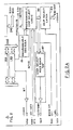
- FIG. 2 is a block diagram of interface 10, in which signal lines on the left side communicate with the bus and signal lines on the right side communicate with the remainder of the peripheral circuit card. For the most part, the signal lines shown, particularly on the left side, are required by the bus architecture described in the publications referred to above.
- imporablytant signal lines are as follows:
- A0-A23 address lines 450-473 indicate to what address a particular data message is directed.
- addresses may be either 24 or 32 bits wide. If an address is 32 bits wide, MADE24 signal line 502 will be inactive so that interface 10 can take the appropriate action, which may be to take no action, to assume that the 8 higher order bits are all zeroes, or to take some other action.
- MADE24 signal line 502 will be inactive so that interface 10 can take the appropriate action, which may be to take no action, to assume that the 8 higher order bits are all zeroes, or to take some other action.
- D0-D7 data lines 400-407 allow the system microprocessor to read and write the configuration registers.
- M/-IO signal 503 is appended to A0-A23 address signals 450-473 to indicate whether the destination address is a memory address or an input/output address. This information is needed in accordance with the referenced bus architecture.
- Control of overall communications between the peripheral circuit board including interface 10 and the bus is handled by board bus and transceiver control circuit 11 which, among other things, controls transceiver 12 which is connected between D0-D7 data lines 400-407 and internal data bus 120 of programmable interface 10.
- Configuration register read/write control circuit 13 controls the setup of the peripheral circuit board by the computer system on power-up, via configuration register read/write lines 130.
- the computer system when the computer system is powered up, it reads identification information from configuration registers 140, 141 to identify the peripheral circuit card.
- Two bytes of card identification number unique to each peripheral circuit card can be read by the system processing unit from configuration registers 140, 141 through the data bus.
- the card identification numbers must be non-volatile such that after power to the system is turned off, the identification information is still stored on the board for the next and subsequent power-up sequences.
- EPROM bits are used as non-volatile registers for identification information.
- Board identification information is programmed on the EPROM bits at the intersections of word line 210 (horizontal line) and bit lines 211 (vertical lines) in arrays 20, 201.
- word line 210 word line for I/O and identification
- bit line 211 vertical lines
- word line 210 word line for I/O and identification
- An erased EPROM bit at the intersection of word line 210 (horizontal line) and bit line 211 results in the bit line being discharged to a logical "0”.
- the logical "0" on the bit line is amplified by the sense amplifier 590 in FIG. 5 (which shows the details of register 140, bit 0 at 140a) and input to tristate buffer 591.
- the identification bit information (logical "0") is transferred to the data bus.
- a programmed EPROM bit will not discharge the bit line to "0".
- the logical "1” will be transferred through sense amplifer 590 to the input of tristate buffer 591 and to the bus in a similar manner.
- identification information is stored in the non-volatile EPROMS and the bit pattern can be read through the data bus when appropriate read signals are activated.
- the computer system retrieves from its mass storage -- usually its system disk drive -- a file containing configuration information for the card, including permissible address ranges for each integrated circuit device on the card. (The file is provided by the card manufacturer and is loaded onto the system drive when the card is installed.) The system does the same thing for each peripheral circuit card it has, determines a conflict-free combination of addresses, and assigns those addresses by obtaining an appropriate address pointer for each desired address range for each card from the configuration file for each card and writing those pointers into one or more of configuration registers 142-145.
- the bus interface on each peripheral circuit card decodes the address (A0-A23) associated with that data to determine whether or not the data is intended for that card.
- Each peripheral circuit card can have several integrated circuit devices on it. Any data transmitted on the system bus is usually intended for only one particular integrated circuit chip or group of chips on one particular card at any one time. Therefore, the bus interface -- interface 10 in the case of a peripheral circuit card using the preferred embodiment of the interface of the invention -- must decode the address and activate, or enable, one integrated circuit device or group of devices on the peripheral circuit card.
- this chip enabling, or "chip select,” function is carried out by dedicated circuitry.
- the chip select function for the first application circuit chip on the peripheral circuit card is carried out by programmable decoder 15 and programmable chip select logic 16.
- the number of decoders and chip select circuits would exactly match the number of integrated circuit devices on the peripheral circuit board.
- interface 10 is a generic, programmable interface, programmable decoder 15 and programmable chip select logic 16 are replicated seven additional times as programmable decoders 150-156 and programmable chip select circuits 160-166, as seen in FIG.
- interface 10 can accommodate up to eight distinctly addressed integrated circuit devices, a particular peripheral circuit card may in fact have as few as one integrated circuit device or groups of devices. Interface 10 also could be designed to handle a smaller or larger maximum number of integrated circuit devices.
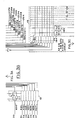
- Programmable chip select logic 16 which, as just described, is programmed for a single integrated circuit device or a group of devices on the peripheral circuit card, has a 52 bit by 8 word (416 bits) CMOS EPROM array 17 which stores up to eight words each of which corresponds to a possible active address range for the integrated circuit device.
- the eight address ranges are selected by the peripheral circuit card designer and are the same address ranges that are provided in the configuration file used by the computer system as described above.
- Each address is 26 bits wide as described above -- A0-A23, M/-IO, and MADE24.
- Array 17 is 52 bits wide because the addresses entered into it are effectively used as "masks" against which incoming address data are matched.
- two bits are required for each address bit.
- Incoming address signals are input to programmable chip select logic 16 at 18, with each input 180 and its complement 181 being supplied to comparator 19.
- Each pair of inputs 180, 181 is provided as an input to comparator 19, part of which is shown in detail at 190.
- the other inputs to comparator 19 are the stored "mask" values representing the corresponding columns in array 17 for whichever row of array 17 is activated by programmable decoder 15, as discussed below, amplified by sense amplifiers 184, 185.
- bits 182, 183 are set to zero and one.
- bits 182, 183 are set to one and zero.
- bits 182, 183 are both set to one.
- a mismatch in a bit -- a one where a zero is sought or vice-versa -- would result in the closing of transistor switch 191, bringing line 192 low.
- the signal on line 192 is input to sense amplifier 199.
- N-channel MOS device 199a and p-channel MOS device 199b form sense amplifier 199.
- Circuit 198 is a voltage biasing circuit generating a volta V REFCS at a level between 0 volts and the V cc supply voltage to the gate of n-channel device 199a. The resulting bias voltage increases the sensitivity of sense amplifier 199.
- the output of sense amplifier 199 is input to latch 193 and output under the control of -ADL signal 501, referred to above, as a chip select signal at 194. If signal 194 is low, then the chip to which chip select logic 16 corresponds is enabled. Otherwise, that chip is not enabled.
- Latch 193 holds output 194 low even after the address input at 18 changes, because in some cases the data transfer on lines D0-D7 is not complete when the address input at 18 changes.
- programmable element 195a of MUX 195 is programmed to a logical "1" which has the effect of bypassing latch 193, so that output 194 instantaneously reflects any change in line 192.
- Line 192 is also fed to a NOR gate 197 along with similar outputs from chip select circuits 160-166. If any one of the integrated circuit devices on the peripheral circuit card is enabled, the output of the NOR gate, available to the bus as the -CDSFDBK signal 507, would go active low. Because the computer operating system knows which card should respond to a particular message, this provides some error checking capability.
- chip select outputs 540-547 may be used to generate useful functions which are not technically chip select signals.
- the peripheral circuit card designer may not want a particular chip select output to contribute to -CDSFDBK signal 507.
- programmable element 196a in MUX 196 could be used to signify that line 192 should not be fed to NOR gate 197 by forcing the corresponding CSTx line to a logical "0".
- chip select outputs may be used to generate latched address outputs for use on the peripheral circuit card by application chips.
- the chip select blocks may also be used to generate feedback signals to the bus such as -CDDS16, which signals to the bus master that the peripheral circuit card has a 16-bit data interface.
- the bus control logic 11, 13 includes in particular the -CDSETUP input 508, the -ADL input 501, the -S0 input 504, the -S1 input 505, the -CMD input 506 and the M/-IO input 503 on the bus side, and the -DEN output 516, the DT/-R output 517, the -IOWR output 515, the -IORD output 514, the -MEMWR output 513, the -MEMRD output 512, the -RDPOS output 510 and the -WRPOS output 511 on the peripheral circuit card side.
- Logic section 11, 13 generates read and write signals 130 for the internal configuration registers 140-145 of programmable interface 10, as well as the peripheral circuit card control signals noted above.
- Blocks 11, 13 are "activated" by either an active -CDSETUP line 508 in conjunction with an I/O Read or Write cycle from the processor (indicating a configuration set-up or configuration cycle), or a valid bus cycle (I/O Read or Write, Memory Read or Write) in conjunction with active -CDSFDBK line 507 (indicating a bus cycle for this peripheral circuit card). This assumes the peripheral circuit card has already been enabled. Otherwise, the outputs of this block remain quiescent.
- Blocks 11, 13 decode the bus cycles as valid combinations of the -S0 signal 504, the -S1 signal 505 and the M/-IO signal 503.
- the coding for these signals is: M/-IO -S0 -S1 Cycle Type 0 0 0 No Op 0 0 1 I/O Write 0 1 0 I/O Read 0 1 1 No Op 1 0 0 No Op 1 0 1 Mem Write 1 1 0 Mem Read 1 1 1 No Op
- the -CMD signal 506 acts as a command strobe and times the generation of the appropriate peripheral circuit card control lines. Therefore, -MEMRD signal 512, -MEMWR signal 513, -IORD signal 514 and -IOWR signal 515 have a duration approximating that of -CMD signal 506.
- DT/-R line 517 controls the direction of data flow through an external data transceiver 60. The external transceiver allows data to flow between the bus and application chips on the peripheral circuit card. DT/-R line 517 changes state after -ADL line 501 falls, and remains latched for the duration of the cycle. It is low for all write cycles.
- -DEN line 516 controls external data transceiver 60 output enables -DEN line 516 is active during a valid Read cycle for essentially the same duration as -CMD line 506.
- a Write cycle however, to give maximum data setup time for the peripheral circuit card, it becomes active a short time after -ADL line 501 falls. It goes inactive after -MEMWR line 513 or -IOWR line 515 goes inactive.
- the peripheral circuit card setup or configuration (sometimes called POST for Power-On Self Test) can occur only when -CDSETUP is active on the rising edge of -ADL signal 501 (address latch input from the bus) followed by an I/O read or write cycle.
- the rising edge of -ADL signal 501 may be used to latch addresses for any type of cycle, and during setup is used to latch A0-A2 lines 450-452 so that the correct configuration register 140-145 may be accessed.
- the -RDPOS signal 510 and -WRPOS signal 511 are used to control optional external configuration register functions. They are valid for any configuration register read or write operation during which -CDSETUP signal 508 is active. The timing for these signals approximates that of -IOWR signal 515 and -IORD signal 514.
- the configuration file information stored in configuration registers 140-145 is accessible through the dedicated transceiver 12 associated with D0-D7 pins 400-407 on the programmable interface chip 10. Data is transferred to the selected configuration register (during a write operation) while -CMD line 506 is low. The rising edge of -CMD signal 506 latches the input data into the register 142-145. Data is read from the configuration registers 140-145 while -CMD line 506 is low, and will become valid at the D0-D7 pins 400-407 within the period specified below from leading (falling) edge of the -CMD signal 506.
- Required configuration registers 140-145 reside in a block at I/O addresses 0100H-0105H for all peripheral circuit cards designed for the bus described above. All registers are byte-wide. Locations 0100H and 0101H are the peripheral circuit card identification number, and are read-only non-volatile EPROM locations. Configuration registers 142-145 are user-defined, with the exception of three bit locations.
- Configuration register 142 Bit 0, at 142a, is used as a card enable bit for all peripheral circuit cards designed for the bus described above. This bit is reset by CHRESET signal 509, or by the processor writing a logical "0" to this bit during a cycle of -CDSETUP signal 508.
- -CDSETUP signal 508 When -CDSETUP signal 508 is a logical "0", the programmable interface chip 10 (and peripheral circuit card) will not respond to any normal bus cycles. Only setup reads and writes are allowed.
- -CDSETUP signal 508 is set to a logical "1" by the processor, normal bus cycles are enabled. This bit may not be written by normal I/O Write operations to address 0102H (register 142).
- the -BDENBL signal 518 on the peripheral circuit card side reflects the state of this bit for peripheral circuit card use.
- Configuration register 145 Bit 7, is used as a channel check flag.
- a peripheral circuit card reports non-maskable interrupts (NMI) to the processor by activating the -CHCK (channel check) line 550, which is wire-ORed to all cards.
- NMI non-maskable interrupts
- Bit 7 is set by a CHRESET signal 509 or a write to register 145 with a logical "1" in the bit 7 position. Bit 7 may also be reset by a write to register 145 with logical "0" data in the bit 7 position.
- Bit 6 of register 145 indicates whether or not channel check exception status is provided in optional configuration registers (not shown). If used, these registers would typically be implemented in components such as external TTL registers (e.g., 74LS374). If channel check exception status is available, a logical "0" will be found in this location. If channel check exception status is not provided, a logical "1" will be found there. If this bit is used for this purpose on the programmable interface chip 10, one of. the programmable POSI/O pins 520-535 on the peripheral circuit card side may be used to force the appropriate value.
- optional configuration registers not shown. If used, these registers would typically be implemented in components such as external TTL registers (e.g., 74LS374). If channel check exception status is available, a logical "0" will be found in this location. If channel check exception status is not provided, a logical "1" will be found there. If this bit is used for this purpose on the programmable interface chip 10, one of.
- bits are user-defineable. These bits may be used for address remapping control or general input or output port functions on the peripheral circuit card (software-controlled "jumpers" or status bits). Each POSI/O pin 520-535 is inde pendently programmable as input or output, and may be assigned to any bit of any configuration register 142-145. The remapping function will be discussed below.
- the chip select logic 16, 160-166 in programmable interface 10 provides up to eight user-programmable chip select outputs 540-547.
- Each chip select output (-CS0-7) may have up to eight pre-programmed address ranges over which it is active. The granularity of these chip selects may range from one location to the entire 16 megabyte physically available 24-bit address range.
- Each chip select output may be defined for either memory or I/O mapping. All 24 A0-A23 bus address lines 450-473, MADE24 signal 502, and the M/-IO input 503, enter the programmable logic arrays.
- An additional input to the programmable chip select arrays may be provided to act as an enable for the chip select function if so desired. Typically, this input would be connected to the MADE24 bus signal 502, to qualify chip selects when 32-bit addressing is involved.
- chip select outputs 540-547 are not latched in any fashion, and are valid only for the duration of a valid address/M/-IO combination on the bus.
- the chip select outputs may be latched by user-programmable flow-through latches using -ADL signal 501. This may be done on an individual chip select basis. This results in the affected chip select output(s) 540-547 going active a short time after -ADL signal 501 has gone active low (the A0-A23 address lines 450-473 and M/-IO input 503 having stabilized well before -ADL signal 501 falls). The outputs are then latched on the rising edge of -ADL signal 501 and remain active until the next bus cycle (-ADL signal 501 goes low again). Latched/non-latched operation for each chip select output is determined by the user when the device is programmed.
- the selection of one of the eight available chip select ranges to be used for a particular chip select output is done by user-defined combinations of bits in configuration registers 142-145.
- a user may define which configuration register bits, and which bit combinations, will activate a given chip select range.
- This information is coded into a programmable decoder 15 in interface 10 which generates an enable for each range.
- the operating system may remap address ranges during the POST if there is a conflict, i.e., two cards which might respond to the same address ranges. This is done by changing (writing) the configuration register bits controlling the chip selects, and hence enabling a new address range.
- the peripheral circuit card designer chooses the allowable address ranges for the various devices on the peripheral circuit card, programs them into array 17, and provides a software file listing the allowable addresses.
- the computer system chooses from among the allowable addresses and writes pointers to the chosen addresses into registers 142-145.
- Interface 10 must decode the contents of registers 142-145 and communicate to chip select logic 16, 160-166 which of the masks in array 17 to use. This function is performed by programmable decoder 15 for the first integrated circuit device on the peripheral circuit card. Decoder 15 is replicated at 150-156 for additional integrated circuit devices on the peripheral circuit card.
- Decoder 15 is a programmable logic array which reads in the information in registers 142-145 and its complement on its word lines, and sends an enable signal on one of its bit lines to the correct row of array 17.
- the correct row of array 17 is the one containing the mask of the address corresponding to the address pointer in registers 142-145.
- the enable signal may be activated by any designer-defined pattern of logical 1's, logical 0's, or "Don't Cares" in registers 142-145, so that each bit as well as it complement are required.
- the programming of the programmable interconnections between the word lines and the bit lines for each decoder 15, 150-156 determines which bit line will be enabled for a particular address pointer stored in registers 142-145.
- connection of any of the 32 configuration register bits with the 16 dedicated POSI/O pins 520-535 on the peripheral circuit card side is controlled by a user-programmable crosspoint switch 100.
- Each POSI/O pin has an open drain output structure as well as an input path.
- a programmable matrix takes the output of any of the configuration register bits and assigns it to any of the 16 output lines. Since the pins are open drain, if a logical "1" is written to a given configuration register bit from the bus, the associated I/O pin is not driven. This allows the I/O pin to be driven by an external signal source, and subsequently for its value to be read through the corresponding configuration register bit location. Forcing a value from the POSI/O pins does not, however, change the value in the configuration register location (see FIG. 4).
- the peripheral circuit card designer may want certain data stored in configuration registers 142-145 to be available to devices on the peripheral circuit card, or to the computer system bus itself. According to the bus architecture described above, the seventh bit in register 145 must be available to the bus as the -CHCK 550 signal, as shown. However, the peripheral circuit card designer may want other data to be available.
- This function is performed by programmable crosspoint matrix 100.
- Matrix 100 is divided into two programmable logic arrays 101, 102.
- Matrix 101 makes data from registers 142-145 available to selected locations on the peripheral circuit card in accordance with the programming of its programmable interconnections, as designed by the peripheral circuit card designer.
- Matrix 102 similarly makes available certain data, in accordance with its programming, to the computer system data bus, via data lines D0-D7.
- Matrix 101 is a programmable crosspoint matrix implemented as a programmable logic array of the type described generally in Spencer, Jr. U.S. Patent 3,566,153, Birkner et al. U.S. Patent 4,124,899, Hartmann et al. U.S. Patent 4,609,986, and Hartmann et al. U.S. Patent 4,617,479, which are hereby incorporated by reference in their entirety.
- EPROM technology is used.
- the same function can be achieved by using EEPROM, fuses or non-volatile register cells.
- Data from each bit of registers 142-145 is connected to the TRUE wordline (WL) and complement wordline (WLN) drivers of the programmable logic array.
- the TRUE wordlines and complement wordlines are connected to the gates of EPROM devices.
- the drain connections of the EPROMs are connected to the various bit lines and the logical-NOR function outputs appear on the outputs of the sense amplifiers 103.
- all EPROM cells connected to the TRUE wordlines are programmed, so that they do not participate in the logic function.
- EPROM bits are programmed by the user using an external programmer prior to being used in the system.
- in-system programming methods can be employed.
- the cross-point matrix connection is made by the EPROM cell located in the intersection of the complement wordline and the bit line corresponding to a particular unprogrammed POSI/0. Usually, all other EPROM cells of the bit line are programmed.
- Locations of unprogrammed EPROM cells determine which bits of the registers are connected to the output. The following description gives an example of a particular connection.
- a logical "1" in bit 0 of register 142 results in a logical "0" on WLN.
- the corresponding bit line is not discharged to zero, resulting a logical "1” in the output of sense amplifier 1C3.
- a logical "0" appears on the gate of open drain output transistor, thus turning the transistor off.
- the line is connected through a pull-up resistor to the power supply. The pull up resistor pulls the POSI/Ox node up to a logical "1".
- FIG. 4 shows the logic representation of a bit in each register 142-145.
- POSI/Ox When POSI/Ox is selected as an output-only pin, its corresponding EPROM cell in matrix 102, used as an I/O architecture control, is left erased.
- the logic level at node A in FIG. 4 then is always a logical "0", allowing data Q from the register bit to pass through the tristate buffer to the data bus when the RD10X line is activated.
- a logical "1" is written into the particular bit of the register associated with a particular POSI/Ox through the crosspoint matrix 101. As described above, that turns off the open drain output transistor, allowing the particular pin to be used as an input line.
- An input signal applied to a POSI/Ox configured as an input goes through crosspoint matrix 102.
- the connection operation through crosspoint matrix 102 is similar to that of matrix 101 described above.
- signals can either be written to the data bus from the POSI/Ox pin through crosspoint matrix 102 by writing a logical "1" to the register in a configuration cycle, or data can be read from the bus through the register to the POSI/0x pin if a logical "0" is written into the register in a configuration cycle.
- Programmable devices 15, 17, 101, 102 are all programmable logic devices of the types described generally in Spencer, Jr. U.S. Patent 3,566,153, Birkner et al. U.S. Patent 4,124,899, Hartmann et al. U.S. Patent 4,609,986, and Hartmann et al. U.S. Patent 4,617,479, which are hereby incorporated by reference in their entirety.
- the programmable interconnections in such devices can be programmed by addressing the appropriate bit line and word line, applying the desired programming data, and transferring that data to the interconnection by applying to a programming pin a voltage significantly higher than the voltage representing a logical 1 -- e.g., 12 volts as opposed to 5 volts in a TTL system.
Landscapes
- Engineering & Computer Science (AREA)
- Theoretical Computer Science (AREA)
- Physics & Mathematics (AREA)
- General Engineering & Computer Science (AREA)
- General Physics & Mathematics (AREA)
- Microcomputers (AREA)
- Logic Circuits (AREA)
Applications Claiming Priority (2)
| Application Number | Priority Date | Filing Date | Title |
|---|---|---|---|
| US07/222,565 US5111423A (en) | 1988-07-21 | 1988-07-21 | Programmable interface for computer system peripheral circuit card |
| US222565 | 1988-07-21 |
Publications (3)
| Publication Number | Publication Date |
|---|---|
| EP0351984A2 true EP0351984A2 (fr) | 1990-01-24 |
| EP0351984A3 EP0351984A3 (fr) | 1991-05-08 |
| EP0351984B1 EP0351984B1 (fr) | 1995-01-18 |
Family
ID=22832737
Family Applications (1)
| Application Number | Title | Priority Date | Filing Date |
|---|---|---|---|
| EP89306840A Expired - Lifetime EP0351984B1 (fr) | 1988-07-21 | 1989-07-06 | Interface programmable pour carte de circuit périphérique de système d'ordinateur |
Country Status (4)
| Country | Link |
|---|---|
| US (1) | US5111423A (fr) |
| EP (1) | EP0351984B1 (fr) |
| JP (1) | JPH02161549A (fr) |
| DE (1) | DE68920652D1 (fr) |
Cited By (2)
| Publication number | Priority date | Publication date | Assignee | Title |
|---|---|---|---|---|
| EP1067459A3 (fr) * | 1993-04-30 | 2001-02-07 | Packard Bell NEC, Inc. | Système de multitraitement symétrique à environnement unifié et fonctions de système répartis |
| WO2002073420A3 (fr) * | 2001-03-13 | 2004-02-05 | Adc Telecomm Israel Ltd | Interface bus pour dispositif d'entree-sortie dote d'une memoire |
Families Citing this family (171)
| Publication number | Priority date | Publication date | Assignee | Title |
|---|---|---|---|---|
| US5450570A (en) * | 1988-09-09 | 1995-09-12 | Compaq Computer Corp. | Computer implemented method and apparatus for dynamic configuration of a computer system and circuit boards including computer resource allocation conflict resolution |
| US5162675A (en) * | 1989-04-14 | 1992-11-10 | Digital Communications Associates, Inc. | Dual personal computer architecture peripheral adapter board and circuit |
| US5317721A (en) * | 1989-11-06 | 1994-05-31 | Zenith Data Systems Corporation | Method and apparatus to disable ISA devices for EISA addresses outside the ISA range |
| US6240496B1 (en) * | 1989-11-24 | 2001-05-29 | Hyundai Electronics America | Architecture and configuring method for a computer expansion board |
| US6751696B2 (en) | 1990-04-18 | 2004-06-15 | Rambus Inc. | Memory device having a programmable register |
| IL96808A (en) * | 1990-04-18 | 1996-03-31 | Rambus Inc | Introductory / Origin Circuit Agreed Using High-Performance Brokerage |
| JPH0823856B2 (ja) * | 1991-02-22 | 1996-03-06 | インターナショナル・ビジネス・マシーンズ・コーポレイション | コンピュータシステムおよびその動作方法 |
| GB9108599D0 (en) * | 1991-04-22 | 1991-06-05 | Pilkington Micro Electronics | Peripheral controller |
| US5274771A (en) * | 1991-04-30 | 1993-12-28 | Hewlett-Packard Company | System for configuring an input/output board in a computer |
| US5367640A (en) * | 1991-04-30 | 1994-11-22 | Hewlett-Packard Company | System for configuring an input/output board in a computer |
| US5315636A (en) * | 1991-06-28 | 1994-05-24 | Network Access Corporation | Personal telecommunications system |
| GB2258069B (en) * | 1991-07-25 | 1995-03-29 | Intel Corp | High speed computer graphics bus |
| US5361336A (en) * | 1991-11-21 | 1994-11-01 | Hewlett-Packard Company | Method for controlling an instrument through a common instrument programming interface |
| FR2687489A1 (fr) * | 1992-02-13 | 1993-08-20 | Hewlett Packard Co | Bus de connexion de cartes d'extension a un systeme informatique et procede de test. |
| US5426739A (en) * | 1992-03-16 | 1995-06-20 | Opti, Inc. | Local bus - I/O Bus Computer Architecture |
| US5345564A (en) * | 1992-03-31 | 1994-09-06 | Zilog, Inc. | Serial communication peripheral integrated electronic circuit that recognizes its unique address before the entire circuit is enabled |
| TW276312B (fr) * | 1992-10-20 | 1996-05-21 | Cirrlis Logic Inc | |
| US5490254A (en) * | 1992-11-04 | 1996-02-06 | United Technologies Corporation | MIL-STD-1553 interface device having autonomous operation in all modes |
| US5367641A (en) * | 1992-11-04 | 1994-11-22 | United Technologies Corporation | MIL-STD-1553 interface device having a bus controller minor frame timer |
| US5325359A (en) * | 1992-11-04 | 1994-06-28 | United Technologies Corporation | MIL-STD-1553 interface device having concurrent remote terminal and monitor terminal operation |
| US5996027A (en) * | 1992-12-18 | 1999-11-30 | Intel Corporation | Transmitting specific command during initial configuration step for configuring disk drive controller |
| US5542092A (en) * | 1993-01-27 | 1996-07-30 | Accton Technology Corporation | Method and system for setting bus addresses in order to resolve or prevent bus address conflicts between interface cards of a personal computer |
| US5497475A (en) * | 1993-02-05 | 1996-03-05 | National Semiconductor Corporation | Configurable integrated circuit having true and shadow EPROM registers |
| US5537607A (en) * | 1993-04-28 | 1996-07-16 | International Business Machines Corporation | Field programmable general purpose interface adapter for connecting peripheral devices within a computer system |
| US5490279A (en) * | 1993-05-21 | 1996-02-06 | Intel Corporation | Method and apparatus for operating a single CPU computer system as a multiprocessor system |
| DE4319985A1 (de) * | 1993-06-11 | 1993-11-18 | Uwe Erpel | Vorrichtung zur Manipulation von Signalen, die über ein Bussystem übertragen werden |
| US5420987A (en) * | 1993-07-19 | 1995-05-30 | 3 Com Corporation | Method and apparatus for configuring a selected adapter unit on a common bus in the presence of other adapter units |
| US5594879A (en) * | 1993-10-29 | 1997-01-14 | Compaq Computer Corporation | Method of and apparatus for arbitrarily disabling under processor control individual slots on a computer bus |
| US5717955A (en) * | 1993-12-03 | 1998-02-10 | Xerox Corporation | System for changing device from specialized interface that enables control of subsystem to general interface that performs general purpose computing functions unrelated to the subsystem |
| DE69428512T2 (de) * | 1993-12-30 | 2002-05-29 | Ncr International, Inc. | Konfigurationsverfahren für Rechnerperipheriegeräte |
| US5764995A (en) * | 1994-03-25 | 1998-06-09 | Packard Bell Nec | Write once read only registers |
| US5517646A (en) * | 1994-04-25 | 1996-05-14 | Compaq Computer Corp. | Expansion device configuration system having two configuration modes which uses automatic expansion configuration sequence during first mode and configures the device individually during second mode |
| US5664231A (en) * | 1994-04-29 | 1997-09-02 | Tps Electronics | PCMCIA interface card for coupling input devices such as barcode scanning engines to personal digital assistants and palmtop computers |
| US5847955A (en) * | 1994-05-04 | 1998-12-08 | National Instruments Corporation | System and method for controlling an instrumentation system |
| US5717614A (en) * | 1994-05-04 | 1998-02-10 | National Instruments Corporation | System and method for handling events in an instrumentation system |
| US5768542A (en) * | 1994-06-08 | 1998-06-16 | Intel Corporation | Method and apparatus for automatically configuring circuit cards in a computer system |
| US5740450A (en) * | 1994-07-26 | 1998-04-14 | United Microelectronics Corporation | Method to automatically detect the interrupt channel status of an add-on card |
| US5727005A (en) * | 1994-08-31 | 1998-03-10 | Le; Chinh H. | Integrated circuit microprocessor with programmable memory access interface types |
| US5617559A (en) * | 1994-08-31 | 1997-04-01 | Motorola Inc. | Modular chip select control circuit and method for performing pipelined memory accesses |
| AU4504796A (en) * | 1994-11-14 | 1996-06-06 | Parallel Technologies, Inc. | Method and apparatus for parallel port interconnection |
| EP0718751A3 (fr) * | 1994-12-23 | 1997-02-12 | Ibm | Dispositif de circuit électronique utilisant un petit lecteur de disques avec un interface reconfigurable |
| JP3115820B2 (ja) * | 1995-05-17 | 2000-12-11 | 松下電器産業株式会社 | インターフェース装置、及びこれを用いたコンピュータ装置 |
| US5668419A (en) * | 1995-06-30 | 1997-09-16 | Canon Information Systems, Inc. | Reconfigurable connector |
| US5724529A (en) * | 1995-11-22 | 1998-03-03 | Cirrus Logic, Inc. | Computer system with multiple PC card controllers and a method of controlling I/O transfers in the system |
| US5915102A (en) * | 1996-11-06 | 1999-06-22 | International Business Machines Corporation | Common arbiter interface device with arbitration configuration for centralized common bus arbitration |
| US5938740A (en) * | 1997-04-21 | 1999-08-17 | Primax Electronics Ltd. | Programmable peripheral control device for controlling peripherals of a computer system |
| US6195593B1 (en) | 1997-09-03 | 2001-02-27 | Seiko Epson Corporation | Reusable modules for complex integrated circuit devices |
| US6049837A (en) * | 1997-12-08 | 2000-04-11 | International Business Machines Corporation | Programmable output interface for lower level open system interconnection architecture |
| US7734852B1 (en) | 1998-08-06 | 2010-06-08 | Ahern Frank W | Modular computer system |
| US6088752A (en) * | 1998-08-06 | 2000-07-11 | Mobility Electronics, Inc. | Method and apparatus for exchanging information between buses in a portable computer and docking station through a bridge employing a serial link |
| US6070214A (en) * | 1998-08-06 | 2000-05-30 | Mobility Electronics, Inc. | Serially linked bus bridge for expanding access over a first bus to a second bus |
| US7269680B1 (en) * | 1998-08-06 | 2007-09-11 | Tao Logic Systems Llc | System enabling device communication in an expanded computing device |
| US6466994B1 (en) * | 1999-03-31 | 2002-10-15 | International Business Machines Corporation | Method and system for programming a system board using a peripheral controller |
| US6728814B2 (en) * | 2000-02-09 | 2004-04-27 | Raytheon Company | Reconfigurable IEEE 1149.1 bus interface |
| JP2003523575A (ja) | 2000-02-14 | 2003-08-05 | モビラティ、イレクトラニクス、インク | 結合システムおよび方法 |
| EP1653373B1 (fr) | 2000-02-14 | 2013-11-13 | Tao Logic Systems LLC | Pont de bus |
| US8645137B2 (en) | 2000-03-16 | 2014-02-04 | Apple Inc. | Fast, language-independent method for user authentication by voice |
| US6594719B1 (en) | 2000-04-19 | 2003-07-15 | Mobility Electronics Inc. | Extended cardbus/pc card controller with split-bridge ™technology |
| JP2002197049A (ja) * | 2000-12-26 | 2002-07-12 | Sharp Corp | マイクロコンピュータ |
| US7076595B1 (en) * | 2001-05-18 | 2006-07-11 | Xilinx, Inc. | Programmable logic device including programmable interface core and central processing unit |
| US20030145137A1 (en) * | 2002-01-27 | 2003-07-31 | Huckins Jeffrey L. | Partially integrating components of processor-based systems |
| US7047335B2 (en) * | 2002-07-25 | 2006-05-16 | Lsi Logic Corporation | Method for receiving user defined frame information structure (FIS) types in a serial-ATA (SATA) system |
| JP2006242638A (ja) * | 2005-03-01 | 2006-09-14 | Matsushita Electric Ind Co Ltd | 半導体検査装置 |
| US8677377B2 (en) | 2005-09-08 | 2014-03-18 | Apple Inc. | Method and apparatus for building an intelligent automated assistant |
| US9318108B2 (en) | 2010-01-18 | 2016-04-19 | Apple Inc. | Intelligent automated assistant |
| US8977255B2 (en) | 2007-04-03 | 2015-03-10 | Apple Inc. | Method and system for operating a multi-function portable electronic device using voice-activation |
| US9330720B2 (en) | 2008-01-03 | 2016-05-03 | Apple Inc. | Methods and apparatus for altering audio output signals |
| US8996376B2 (en) | 2008-04-05 | 2015-03-31 | Apple Inc. | Intelligent text-to-speech conversion |
| US10496753B2 (en) | 2010-01-18 | 2019-12-03 | Apple Inc. | Automatically adapting user interfaces for hands-free interaction |
| US20100030549A1 (en) | 2008-07-31 | 2010-02-04 | Lee Michael M | Mobile device having human language translation capability with positional feedback |
| US8154942B1 (en) | 2008-11-17 | 2012-04-10 | Altera Corporation | Integrated circuits with fuse programming and sensing circuitry |
| US9959870B2 (en) | 2008-12-11 | 2018-05-01 | Apple Inc. | Speech recognition involving a mobile device |
| US10241752B2 (en) | 2011-09-30 | 2019-03-26 | Apple Inc. | Interface for a virtual digital assistant |
| US10255566B2 (en) | 2011-06-03 | 2019-04-09 | Apple Inc. | Generating and processing task items that represent tasks to perform |
| US9858925B2 (en) | 2009-06-05 | 2018-01-02 | Apple Inc. | Using context information to facilitate processing of commands in a virtual assistant |
| US10241644B2 (en) | 2011-06-03 | 2019-03-26 | Apple Inc. | Actionable reminder entries |
| US9431006B2 (en) | 2009-07-02 | 2016-08-30 | Apple Inc. | Methods and apparatuses for automatic speech recognition |
| US10276170B2 (en) | 2010-01-18 | 2019-04-30 | Apple Inc. | Intelligent automated assistant |
| US10679605B2 (en) | 2010-01-18 | 2020-06-09 | Apple Inc. | Hands-free list-reading by intelligent automated assistant |
| US10705794B2 (en) | 2010-01-18 | 2020-07-07 | Apple Inc. | Automatically adapting user interfaces for hands-free interaction |
| US10553209B2 (en) | 2010-01-18 | 2020-02-04 | Apple Inc. | Systems and methods for hands-free notification summaries |
| DE202011111062U1 (de) | 2010-01-25 | 2019-02-19 | Newvaluexchange Ltd. | Vorrichtung und System für eine Digitalkonversationsmanagementplattform |
| US8682667B2 (en) | 2010-02-25 | 2014-03-25 | Apple Inc. | User profiling for selecting user specific voice input processing information |
| US10762293B2 (en) | 2010-12-22 | 2020-09-01 | Apple Inc. | Using parts-of-speech tagging and named entity recognition for spelling correction |
| US9262612B2 (en) | 2011-03-21 | 2016-02-16 | Apple Inc. | Device access using voice authentication |
| US10057736B2 (en) | 2011-06-03 | 2018-08-21 | Apple Inc. | Active transport based notifications |
| US8994660B2 (en) | 2011-08-29 | 2015-03-31 | Apple Inc. | Text correction processing |
| US10134385B2 (en) | 2012-03-02 | 2018-11-20 | Apple Inc. | Systems and methods for name pronunciation |
| US9483461B2 (en) | 2012-03-06 | 2016-11-01 | Apple Inc. | Handling speech synthesis of content for multiple languages |
| US9280610B2 (en) | 2012-05-14 | 2016-03-08 | Apple Inc. | Crowd sourcing information to fulfill user requests |
| US9721563B2 (en) | 2012-06-08 | 2017-08-01 | Apple Inc. | Name recognition system |
| US9495129B2 (en) | 2012-06-29 | 2016-11-15 | Apple Inc. | Device, method, and user interface for voice-activated navigation and browsing of a document |
| US9576574B2 (en) | 2012-09-10 | 2017-02-21 | Apple Inc. | Context-sensitive handling of interruptions by intelligent digital assistant |
| US9547647B2 (en) | 2012-09-19 | 2017-01-17 | Apple Inc. | Voice-based media searching |
| DE112014000709B4 (de) | 2013-02-07 | 2021-12-30 | Apple Inc. | Verfahren und vorrichtung zum betrieb eines sprachtriggers für einen digitalen assistenten |
| US9368114B2 (en) | 2013-03-14 | 2016-06-14 | Apple Inc. | Context-sensitive handling of interruptions |
| WO2014144949A2 (fr) | 2013-03-15 | 2014-09-18 | Apple Inc. | Entraînement d'un système à commande au moins partiellement vocale |
| WO2014144579A1 (fr) | 2013-03-15 | 2014-09-18 | Apple Inc. | Système et procédé pour mettre à jour un modèle de reconnaissance de parole adaptatif |
| WO2014197334A2 (fr) | 2013-06-07 | 2014-12-11 | Apple Inc. | Système et procédé destinés à une prononciation de mots spécifiée par l'utilisateur dans la synthèse et la reconnaissance de la parole |
| US9582608B2 (en) | 2013-06-07 | 2017-02-28 | Apple Inc. | Unified ranking with entropy-weighted information for phrase-based semantic auto-completion |
| WO2014197336A1 (fr) | 2013-06-07 | 2014-12-11 | Apple Inc. | Système et procédé pour détecter des erreurs dans des interactions avec un assistant numérique utilisant la voix |
| WO2014197335A1 (fr) | 2013-06-08 | 2014-12-11 | Apple Inc. | Interprétation et action sur des commandes qui impliquent un partage d'informations avec des dispositifs distants |
| US10176167B2 (en) | 2013-06-09 | 2019-01-08 | Apple Inc. | System and method for inferring user intent from speech inputs |
| KR101959188B1 (ko) | 2013-06-09 | 2019-07-02 | 애플 인크. | 디지털 어시스턴트의 둘 이상의 인스턴스들에 걸친 대화 지속성을 가능하게 하기 위한 디바이스, 방법 및 그래픽 사용자 인터페이스 |
| KR101809808B1 (ko) | 2013-06-13 | 2017-12-15 | 애플 인크. | 음성 명령에 의해 개시되는 긴급 전화를 걸기 위한 시스템 및 방법 |
| KR101749009B1 (ko) | 2013-08-06 | 2017-06-19 | 애플 인크. | 원격 디바이스로부터의 활동에 기초한 스마트 응답의 자동 활성화 |
| US9620105B2 (en) | 2014-05-15 | 2017-04-11 | Apple Inc. | Analyzing audio input for efficient speech and music recognition |
| US10592095B2 (en) | 2014-05-23 | 2020-03-17 | Apple Inc. | Instantaneous speaking of content on touch devices |
| US9502031B2 (en) | 2014-05-27 | 2016-11-22 | Apple Inc. | Method for supporting dynamic grammars in WFST-based ASR |
| WO2015184186A1 (fr) | 2014-05-30 | 2015-12-03 | Apple Inc. | Procédé d'entrée à simple énoncé multi-commande |
| US9842101B2 (en) | 2014-05-30 | 2017-12-12 | Apple Inc. | Predictive conversion of language input |
| US10170123B2 (en) | 2014-05-30 | 2019-01-01 | Apple Inc. | Intelligent assistant for home automation |
| US9785630B2 (en) | 2014-05-30 | 2017-10-10 | Apple Inc. | Text prediction using combined word N-gram and unigram language models |
| US10078631B2 (en) | 2014-05-30 | 2018-09-18 | Apple Inc. | Entropy-guided text prediction using combined word and character n-gram language models |
| US9633004B2 (en) | 2014-05-30 | 2017-04-25 | Apple Inc. | Better resolution when referencing to concepts |
| US9430463B2 (en) | 2014-05-30 | 2016-08-30 | Apple Inc. | Exemplar-based natural language processing |
| US10289433B2 (en) | 2014-05-30 | 2019-05-14 | Apple Inc. | Domain specific language for encoding assistant dialog |
| US9715875B2 (en) | 2014-05-30 | 2017-07-25 | Apple Inc. | Reducing the need for manual start/end-pointing and trigger phrases |
| US9734193B2 (en) | 2014-05-30 | 2017-08-15 | Apple Inc. | Determining domain salience ranking from ambiguous words in natural speech |
| US9760559B2 (en) | 2014-05-30 | 2017-09-12 | Apple Inc. | Predictive text input |
| US9338493B2 (en) | 2014-06-30 | 2016-05-10 | Apple Inc. | Intelligent automated assistant for TV user interactions |
| US10659851B2 (en) | 2014-06-30 | 2020-05-19 | Apple Inc. | Real-time digital assistant knowledge updates |
| US10446141B2 (en) | 2014-08-28 | 2019-10-15 | Apple Inc. | Automatic speech recognition based on user feedback |
| US9818400B2 (en) | 2014-09-11 | 2017-11-14 | Apple Inc. | Method and apparatus for discovering trending terms in speech requests |
| US10789041B2 (en) | 2014-09-12 | 2020-09-29 | Apple Inc. | Dynamic thresholds for always listening speech trigger |
| US9668121B2 (en) | 2014-09-30 | 2017-05-30 | Apple Inc. | Social reminders |
| US9646609B2 (en) | 2014-09-30 | 2017-05-09 | Apple Inc. | Caching apparatus for serving phonetic pronunciations |
| US10127911B2 (en) | 2014-09-30 | 2018-11-13 | Apple Inc. | Speaker identification and unsupervised speaker adaptation techniques |
| US9886432B2 (en) | 2014-09-30 | 2018-02-06 | Apple Inc. | Parsimonious handling of word inflection via categorical stem + suffix N-gram language models |
| US10074360B2 (en) | 2014-09-30 | 2018-09-11 | Apple Inc. | Providing an indication of the suitability of speech recognition |
| US10552013B2 (en) | 2014-12-02 | 2020-02-04 | Apple Inc. | Data detection |
| US9711141B2 (en) | 2014-12-09 | 2017-07-18 | Apple Inc. | Disambiguating heteronyms in speech synthesis |
| US9865280B2 (en) | 2015-03-06 | 2018-01-09 | Apple Inc. | Structured dictation using intelligent automated assistants |
| US10567477B2 (en) | 2015-03-08 | 2020-02-18 | Apple Inc. | Virtual assistant continuity |
| US9721566B2 (en) | 2015-03-08 | 2017-08-01 | Apple Inc. | Competing devices responding to voice triggers |
| US9886953B2 (en) | 2015-03-08 | 2018-02-06 | Apple Inc. | Virtual assistant activation |
| US9899019B2 (en) | 2015-03-18 | 2018-02-20 | Apple Inc. | Systems and methods for structured stem and suffix language models |
| US9842105B2 (en) | 2015-04-16 | 2017-12-12 | Apple Inc. | Parsimonious continuous-space phrase representations for natural language processing |
| US10083688B2 (en) | 2015-05-27 | 2018-09-25 | Apple Inc. | Device voice control for selecting a displayed affordance |
| US10127220B2 (en) | 2015-06-04 | 2018-11-13 | Apple Inc. | Language identification from short strings |
| US10101822B2 (en) | 2015-06-05 | 2018-10-16 | Apple Inc. | Language input correction |
| US10186254B2 (en) | 2015-06-07 | 2019-01-22 | Apple Inc. | Context-based endpoint detection |
| US10255907B2 (en) | 2015-06-07 | 2019-04-09 | Apple Inc. | Automatic accent detection using acoustic models |
| US11025565B2 (en) | 2015-06-07 | 2021-06-01 | Apple Inc. | Personalized prediction of responses for instant messaging |
| US10747498B2 (en) | 2015-09-08 | 2020-08-18 | Apple Inc. | Zero latency digital assistant |
| US10671428B2 (en) | 2015-09-08 | 2020-06-02 | Apple Inc. | Distributed personal assistant |
| US9697820B2 (en) | 2015-09-24 | 2017-07-04 | Apple Inc. | Unit-selection text-to-speech synthesis using concatenation-sensitive neural networks |
| US10366158B2 (en) | 2015-09-29 | 2019-07-30 | Apple Inc. | Efficient word encoding for recurrent neural network language models |
| US11010550B2 (en) | 2015-09-29 | 2021-05-18 | Apple Inc. | Unified language modeling framework for word prediction, auto-completion and auto-correction |
| US11587559B2 (en) | 2015-09-30 | 2023-02-21 | Apple Inc. | Intelligent device identification |
| US10691473B2 (en) | 2015-11-06 | 2020-06-23 | Apple Inc. | Intelligent automated assistant in a messaging environment |
| US10049668B2 (en) | 2015-12-02 | 2018-08-14 | Apple Inc. | Applying neural network language models to weighted finite state transducers for automatic speech recognition |
| US10223066B2 (en) | 2015-12-23 | 2019-03-05 | Apple Inc. | Proactive assistance based on dialog communication between devices |
| US10446143B2 (en) | 2016-03-14 | 2019-10-15 | Apple Inc. | Identification of voice inputs providing credentials |
| US9934775B2 (en) | 2016-05-26 | 2018-04-03 | Apple Inc. | Unit-selection text-to-speech synthesis based on predicted concatenation parameters |
| US9972304B2 (en) | 2016-06-03 | 2018-05-15 | Apple Inc. | Privacy preserving distributed evaluation framework for embedded personalized systems |
| US10249300B2 (en) | 2016-06-06 | 2019-04-02 | Apple Inc. | Intelligent list reading |
| US10049663B2 (en) | 2016-06-08 | 2018-08-14 | Apple, Inc. | Intelligent automated assistant for media exploration |
| DK179588B1 (en) | 2016-06-09 | 2019-02-22 | Apple Inc. | INTELLIGENT AUTOMATED ASSISTANT IN A HOME ENVIRONMENT |
| US10490187B2 (en) | 2016-06-10 | 2019-11-26 | Apple Inc. | Digital assistant providing automated status report |
| US10192552B2 (en) | 2016-06-10 | 2019-01-29 | Apple Inc. | Digital assistant providing whispered speech |
| US10067938B2 (en) | 2016-06-10 | 2018-09-04 | Apple Inc. | Multilingual word prediction |
| US10586535B2 (en) | 2016-06-10 | 2020-03-10 | Apple Inc. | Intelligent digital assistant in a multi-tasking environment |
| US10509862B2 (en) | 2016-06-10 | 2019-12-17 | Apple Inc. | Dynamic phrase expansion of language input |
| DK201670540A1 (en) | 2016-06-11 | 2018-01-08 | Apple Inc | Application integration with a digital assistant |
| DK179343B1 (en) | 2016-06-11 | 2018-05-14 | Apple Inc | Intelligent task discovery |
| DK179415B1 (en) | 2016-06-11 | 2018-06-14 | Apple Inc | Intelligent device arbitration and control |
| DK179049B1 (en) | 2016-06-11 | 2017-09-18 | Apple Inc | Data driven natural language event detection and classification |
| US10593346B2 (en) | 2016-12-22 | 2020-03-17 | Apple Inc. | Rank-reduced token representation for automatic speech recognition |
| DK179745B1 (en) | 2017-05-12 | 2019-05-01 | Apple Inc. | SYNCHRONIZATION AND TASK DELEGATION OF A DIGITAL ASSISTANT |
| DK201770431A1 (en) | 2017-05-15 | 2018-12-20 | Apple Inc. | Optimizing dialogue policy decisions for digital assistants using implicit feedback |
Family Cites Families (40)
| Publication number | Priority date | Publication date | Assignee | Title |
|---|---|---|---|---|
| US3566153A (en) * | 1969-04-30 | 1971-02-23 | Texas Instruments Inc | Programmable sequential logic |
| US4006466A (en) * | 1975-03-26 | 1977-02-01 | Honeywell Information Systems, Inc. | Programmable interface apparatus and method |
| US4034354A (en) * | 1975-11-21 | 1977-07-05 | The Bendix Corporation | Programmable interface controller for numerical machine systems |
| US4124899A (en) * | 1977-05-23 | 1978-11-07 | Monolithic Memories, Inc. | Programmable array logic circuit |
| US4144561A (en) * | 1977-07-08 | 1979-03-13 | Xerox Corporation | Chip topography for MOS integrated circuitry microprocessor chip |
| US4127896A (en) * | 1977-08-10 | 1978-11-28 | Bunker Ramo Corporation | Bidirectional interface utilizing read-only memory, decoder and multiplexer |
| US4156796A (en) * | 1977-11-29 | 1979-05-29 | International Business Machines Corporation | Programmable data processing communications multiplexer |
| US4188665A (en) * | 1977-11-29 | 1980-02-12 | International Business Machines Corporation | Programmable communications subsystem |
| US4179738A (en) * | 1978-06-23 | 1979-12-18 | International Business Machines Corporation | Programmable control latch mechanism for a data processing system |
| US4225919A (en) * | 1978-06-30 | 1980-09-30 | Motorola, Inc. | Advanced data link controller |
| US4254473A (en) * | 1979-01-29 | 1981-03-03 | Allen-Bradley Company | Rack adapter for serially connected I/O interface racks |
| US4794558A (en) * | 1979-06-12 | 1988-12-27 | Motorola, Inc. | Microprocessor having self-programmed eprom |
| DE2939411C2 (de) * | 1979-09-28 | 1982-09-02 | Siemens AG, 1000 Berlin und 8000 München | Datenverarbeitungsanlage mit virtueller Speicheradressierung |
| US4334157A (en) * | 1980-02-22 | 1982-06-08 | Fairchild Camera And Instrument Corp. | Data latch with enable signal gating |
| US4393443A (en) * | 1980-05-20 | 1983-07-12 | Tektronix, Inc. | Memory mapping system |
| US4443845A (en) * | 1980-06-26 | 1984-04-17 | Texas Instruments Incorporated | Memory system having a common interface |
| US4390963A (en) * | 1980-09-15 | 1983-06-28 | Motorola, Inc. | Interface adapter architecture |
| US4442502A (en) * | 1981-03-30 | 1984-04-10 | Datapoint Corporation | Digital information switching system |
| US4400794A (en) * | 1981-11-17 | 1983-08-23 | Burroughs Corporation | Memory mapping unit |
| US4473878A (en) * | 1981-11-23 | 1984-09-25 | Motorola, Inc. | Memory management unit |
| US4488256A (en) * | 1981-11-23 | 1984-12-11 | Motorola, Inc. | Memory management unit having means for detecting and preventing mapping conflicts |
| JPS58102381A (ja) * | 1981-12-15 | 1983-06-17 | Nec Corp | バツフアメモリ |
| US4670855A (en) * | 1982-02-24 | 1987-06-02 | Digital Equipment Corporation | Interchangeable interface circuit structure |
| US4453229A (en) * | 1982-03-11 | 1984-06-05 | Grumman Aerospace Corporation | Bus interface unit |
| BG35575A1 (en) * | 1982-04-26 | 1984-05-15 | Kasabov | Multimicroprocessor system |
| US4485439A (en) * | 1982-07-27 | 1984-11-27 | S.A. Analis | Standard hardware-software interface for connecting any instrument which provides a digital output stream with any digital host computer |
| US4625308A (en) * | 1982-11-30 | 1986-11-25 | American Satellite Company | All digital IDMA dynamic channel allocated satellite communications system and method |
| US4751671A (en) * | 1983-02-14 | 1988-06-14 | Prime Computer, Inc. | Size configurable data storage system |
| US4638451A (en) * | 1983-05-03 | 1987-01-20 | Texas Instruments Incorporated | Microprocessor system with programmable interface |
| US4587609A (en) * | 1983-07-01 | 1986-05-06 | Honeywell Information Systems Inc. | Lockout operation among asynchronous accessers of a shared computer system resource |
| US4675808A (en) * | 1983-08-08 | 1987-06-23 | American Telephone And Telegraph Company At&T Bell Laboratories | Multiplexed-address interface for addressing memories of various sizes |
| US4570220A (en) * | 1983-11-25 | 1986-02-11 | Intel Corporation | High speed parallel bus and data transfer method |
| DE3347357A1 (de) * | 1983-12-28 | 1985-07-11 | Siemens AG, 1000 Berlin und 8000 München | Einrichtung zum vergeben von adressen an steckbare baugruppen |
| US4617479B1 (en) * | 1984-05-03 | 1993-09-21 | Altera Semiconductor Corp. | Programmable logic array device using eprom technology |
| US4609986A (en) * | 1984-06-14 | 1986-09-02 | Altera Corporation | Programmable logic array device using EPROM technology |
| US4670748A (en) * | 1985-08-09 | 1987-06-02 | Harris Corporation | Programmable chip select decoder |
| US4920483A (en) * | 1985-11-15 | 1990-04-24 | Data General Corporation | A computer memory for accessing any word-sized group of contiguous bits |
| US4853846A (en) * | 1986-07-29 | 1989-08-01 | Intel Corporation | Bus expander with logic for virtualizing single cache control into dual channels with separate directories and prefetch for different processors |
| US4727977A (en) * | 1986-08-18 | 1988-03-01 | Arnson Robert S | Cover for a grain conveyor hopper |
| US4825054A (en) * | 1988-02-16 | 1989-04-25 | Datacard Corporation | Method and apparatus for parallel integrated circuit card initialization and embossing |
-
1988
- 1988-07-21 US US07/222,565 patent/US5111423A/en not_active Expired - Lifetime
-
1989
- 1989-07-06 EP EP89306840A patent/EP0351984B1/fr not_active Expired - Lifetime
- 1989-07-06 DE DE68920652T patent/DE68920652D1/de not_active Expired - Lifetime
- 1989-07-20 JP JP1186182A patent/JPH02161549A/ja active Pending
Cited By (3)
| Publication number | Priority date | Publication date | Assignee | Title |
|---|---|---|---|---|
| EP1067459A3 (fr) * | 1993-04-30 | 2001-02-07 | Packard Bell NEC, Inc. | Système de multitraitement symétrique à environnement unifié et fonctions de système répartis |
| WO2002073420A3 (fr) * | 2001-03-13 | 2004-02-05 | Adc Telecomm Israel Ltd | Interface bus pour dispositif d'entree-sortie dote d'une memoire |
| US6710620B2 (en) | 2001-03-13 | 2004-03-23 | Adc Telecommunications Israel, Ltd. | Bus interface for I/O device with memory |
Also Published As
| Publication number | Publication date |
|---|---|
| US5111423A (en) | 1992-05-05 |
| EP0351984A3 (fr) | 1991-05-08 |
| JPH02161549A (ja) | 1990-06-21 |
| DE68920652D1 (de) | 1995-03-02 |
| EP0351984B1 (fr) | 1995-01-18 |
Similar Documents
| Publication | Publication Date | Title |
|---|---|---|
| EP0351984B1 (fr) | Interface programmable pour carte de circuit périphérique de système d'ordinateur | |
| JP3210660B2 (ja) | プログラマブル論理素子のための論理ブロック | |
| US5402014A (en) | Peripheral port with volatile and non-volatile configuration | |
| US5128559A (en) | Logic block for programmable logic devices | |
| US5809281A (en) | Field programmable gate array with high speed SRAM based configurable function block configurable as high performance logic or block of SRAM | |
| US5737766A (en) | Programmable gate array configuration memory which allows sharing with user memory | |
| US4783606A (en) | Programming circuit for programmable logic array I/O cell | |
| USRE37195E1 (en) | Programmable switch for FPGA input/output signals | |
| US5099150A (en) | Circuit block for programmable logic devices, configurable as a user-writable memory or a logic circuit | |
| US5493531A (en) | Integrated circuitry for checking the utilization rate of redundancy memory elements in a semiconductor memory device | |
| US5812867A (en) | Integrated circuit comprising a microprocessor, a memory and internal configurable peripherals | |
| US20020073372A1 (en) | General port capable of implementing the jtag protocol | |
| US6029236A (en) | Field programmable gate array with high speed SRAM based configurable function block configurable as high performance logic or block of SRAM | |
| JPH04333000A (ja) | 読出専用半導体メモリ装置 | |
| US5548554A (en) | Integrated programming circuitry for an electrically programmable semiconductor memory device with redundancy | |
| US5282164A (en) | Programmable integrated circuit | |
| US5452229A (en) | Programmable integrated-circuit switch | |
| US4646269A (en) | Multiple programmable initialize words in a programmable read only memory | |
| JPH0628528A (ja) | Icカード用インターフェース回路 | |
| US5099453A (en) | Configuration memory for programmable logic device | |
| US7305514B2 (en) | Command sequence for optimized power consumption | |
| US6400611B1 (en) | Independent asynchronous boot block for synchronous non-volatile memory devices | |
| US5046180A (en) | Semiconductor integrated circuit device comprising non-reprogrammable internal memory device | |
| US7904667B2 (en) | Systems and methods for monitoring and controlling binary state devices using a memory device | |
| US6072332A (en) | Variable depth memories for programmable logic devices |
Legal Events
| Date | Code | Title | Description |
|---|---|---|---|
| PUAI | Public reference made under article 153(3) epc to a published international application that has entered the european phase |
Free format text: ORIGINAL CODE: 0009012 |
|
| AK | Designated contracting states |
Kind code of ref document: A2 Designated state(s): DE FR GB IT NL |
|
| PUAL | Search report despatched |
Free format text: ORIGINAL CODE: 0009013 |
|
| AK | Designated contracting states |
Kind code of ref document: A3 Designated state(s): DE FR GB IT NL |
|
| 17P | Request for examination filed |
Effective date: 19910617 |
|
| 17Q | First examination report despatched |
Effective date: 19930622 |
|
| RAP1 | Party data changed (applicant data changed or rights of an application transferred) |
Owner name: ALTERA CORPORATION |
|
| GRAA | (expected) grant |
Free format text: ORIGINAL CODE: 0009210 |
|
| AK | Designated contracting states |
Kind code of ref document: B1 Designated state(s): DE FR GB IT NL |
|
| PG25 | Lapsed in a contracting state [announced via postgrant information from national office to epo] |
Ref country code: IT Free format text: LAPSE BECAUSE OF FAILURE TO SUBMIT A TRANSLATION OF THE DESCRIPTION OR TO PAY THE FEE WITHIN THE PRE;WARNING: LAPSES OF ITALIAN PATENTS WITH EFFECTIVE DATE BEFORE 2007 MAY HAVE OCCURRED AT ANY TIME BEFORE 2007. THE CORRECT EFFECTIVE DATE MAY BE DIFFERENT FROM THE ONE RECORDED.SCRIBED TIME-LIMIT Effective date: 19950118 Ref country code: FR Effective date: 19950118 Ref country code: NL Effective date: 19950118 |
|
| REF | Corresponds to: |
Ref document number: 68920652 Country of ref document: DE Date of ref document: 19950302 |
|
| PG25 | Lapsed in a contracting state [announced via postgrant information from national office to epo] |
Ref country code: DE Effective date: 19950419 |
|
| EN | Fr: translation not filed | ||
| PGFP | Annual fee paid to national office [announced via postgrant information from national office to epo] |
Ref country code: NL Payment date: 19950627 Year of fee payment: 7 |
|
| NLV1 | Nl: lapsed or annulled due to failure to fulfill the requirements of art. 29p and 29m of the patents act | ||
| PLBE | No opposition filed within time limit |
Free format text: ORIGINAL CODE: 0009261 |
|
| STAA | Information on the status of an ep patent application or granted ep patent |
Free format text: STATUS: NO OPPOSITION FILED WITHIN TIME LIMIT |
|
| 26N | No opposition filed | ||
| REG | Reference to a national code |
Ref country code: GB Ref legal event code: 732E |
|
| REG | Reference to a national code |
Ref country code: GB Ref legal event code: IF02 |
|
| PGFP | Annual fee paid to national office [announced via postgrant information from national office to epo] |
Ref country code: GB Payment date: 20040615 Year of fee payment: 16 |
|
| PG25 | Lapsed in a contracting state [announced via postgrant information from national office to epo] |
Ref country code: GB Free format text: LAPSE BECAUSE OF NON-PAYMENT OF DUE FEES Effective date: 20050706 |
|
| GBPC | Gb: european patent ceased through non-payment of renewal fee |
Effective date: 20050706 |