EP0352021A2 - Optischer Verstärker mit reduzierter Nichtlinearität - Google Patents
Optischer Verstärker mit reduzierter Nichtlinearität Download PDFInfo
- Publication number
- EP0352021A2 EP0352021A2 EP89307109A EP89307109A EP0352021A2 EP 0352021 A2 EP0352021 A2 EP 0352021A2 EP 89307109 A EP89307109 A EP 89307109A EP 89307109 A EP89307109 A EP 89307109A EP 0352021 A2 EP0352021 A2 EP 0352021A2
- Authority
- EP
- European Patent Office
- Prior art keywords
- amplifier
- optical
- gain
- signal
- induced
- Prior art date
- Legal status (The legal status is an assumption and is not a legal conclusion. Google has not performed a legal analysis and makes no representation as to the accuracy of the status listed.)
- Granted
Links
Images



Classifications
-
- H—ELECTRICITY
- H03—ELECTRONIC CIRCUITRY
- H03F—AMPLIFIERS
- H03F1/00—Details of amplifiers with only discharge tubes, only semiconductor devices or only unspecified devices as amplifying elements
- H03F1/02—Modifications of amplifiers to raise the efficiency, e.g. gliding Class A stages, use of an auxiliary oscillation
- H03F1/0205—Modifications of amplifiers to raise the efficiency, e.g. gliding Class A stages, use of an auxiliary oscillation in transistor amplifiers
- H03F1/0261—Modifications of amplifiers to raise the efficiency, e.g. gliding Class A stages, use of an auxiliary oscillation in transistor amplifiers with control of the polarisation voltage or current, e.g. gliding Class A
- H03F1/0266—Modifications of amplifiers to raise the efficiency, e.g. gliding Class A stages, use of an auxiliary oscillation in transistor amplifiers with control of the polarisation voltage or current, e.g. gliding Class A by using a signal derived from the input signal
-
- H—ELECTRICITY
- H01—ELECTRIC ELEMENTS
- H01S—DEVICES USING THE PROCESS OF LIGHT AMPLIFICATION BY STIMULATED EMISSION OF RADIATION [LASER] TO AMPLIFY OR GENERATE LIGHT; DEVICES USING STIMULATED EMISSION OF ELECTROMAGNETIC RADIATION IN WAVE RANGES OTHER THAN OPTICAL
- H01S5/00—Semiconductor lasers
- H01S5/06—Arrangements for controlling the laser output parameters, e.g. by operating on the active medium
- H01S5/068—Stabilisation of laser output parameters
- H01S5/0683—Stabilisation of laser output parameters by monitoring the optical output parameters
-
- H—ELECTRICITY
- H01—ELECTRIC ELEMENTS
- H01S—DEVICES USING THE PROCESS OF LIGHT AMPLIFICATION BY STIMULATED EMISSION OF RADIATION [LASER] TO AMPLIFY OR GENERATE LIGHT; DEVICES USING STIMULATED EMISSION OF ELECTROMAGNETIC RADIATION IN WAVE RANGES OTHER THAN OPTICAL
- H01S5/00—Semiconductor lasers
- H01S5/50—Amplifier structures not provided for in groups H01S5/02 - H01S5/30
Definitions
- This invention relates to optical amplifiers, and to optical communication systems utilizing such optical amplifiers.
- Optical amplifiers are emerging as practical components for use in various lightwave communication systems. Such optical amplifiers can enhance the performance of lightwave communication systems by boosting signal levels to overcome noise.
- the gain of such amplifiers, and specifically the gain of preferred semiconductor optical amplifiers is inherently nonlinear. Such nonlinearity can cause adverse, and potentially harmful, effects such as gain saturation, inter-modulation distortion (IMD) in frequency-division-multiplexed (FDM) systems employing closely spaced carriers, crosstalk in wavelength- division-multiplexed (WDM) systems employing widely spaced on-off-keyed (OOK) or amplitude shift keyed (AMK) carriers, and pulse distortion in multi-Gb/s intensity-modulation systems, even those employing a single carrier.
- IMD inter-modulation distortion
- FDM frequency-division-multiplexed
- WDM wavelength- division-multiplexed
- OOK widely spaced on-off-keyed
- AMK amplitude shift keyed
- This invention is an improved optical amplifier with reduced signal-induced nonlinear effects such as crosstalk, inter-modulation distortion and other saturation induced effects.
- a compensation loop such as a feed-forward or feed-back loop, is used to reduce the signal induced saturation, and therefore, the signal induced nonlinearities.
- the loop operates by providing additional, signal-induced pumping to the gain medium associated with the amplifier, thereby compensating for what would otherwise be signal induced variations in the gain of the optical amplifier.
- equalization in the compensation loop is unnecessary because of the inherent equalization associated with the frequency response of the gain medium.
- a compensation loop with a substantially flat frequency response is sufficient to compensate adequately for the signal-induced variations in the gain of the optical amplifier.
- the invention is an improved optical amplifier with reduced signal-induced nonlinearities.
- an appropriate compensation loop provides additional, signal-induced pumping to the gain medium thereby compensating for what would otherwise be signal-induced variations in the gain of the optical amplifier.
- the coupled, partial differential, wave and rate equations are used to develop general-purpose small-signal and large-signal nonlinear optical-amplifier models that are much more suitable for communications-systems analysis than previous solutions.
- a practical feed-forward linearization scheme is presented that is capable of significantly reducing signal-induced nonlinear distortions, without reducing the required output power or increasing the desired inter-carrier separation.
- a two-tone circuit which shows a reduction of the inter-modulation distortion by about 14 dB. In effect, this would allow the operation of the amplifier with an increased output power of 7 dB--half the IMD reduction.
- a simple feed-forward circuit is shown to reduce saturation-induced crosstalk in wavelength-multiplexed on-off-keyed optical amplifier applications.
- a two-channel circuit is described which reduces crosstalk by 20 dB while the effective gain of the amplifier is increased by 3 dB.
- the coupled, partial differential, wave and rate equations are used to develop general purpose small-signal and large-signal nonlinear optical-amplifier models that are much more suitable for communications-systems analysis than previous solutions.
- Equations (2) and (4) represent the input-output relations of an amplifier in terms of the three physical constants, ⁇ , ⁇ c and P sat , and the small-signal power gain, exp(Go). In principle, they can be solved iteratively. For example, if one has a reasonable first guess at the output envelope, E out (t), the right-hand side of (4) would be known, and the differential equation can be solved for G(t).
- G(t)-Go can be considered as the output response of a low-pass R-C filter with a time constant of ⁇ c , i.e., a frequency response of 1/(1 +j ⁇ ⁇ c ), with the right-hand side of (4) as an input.
- F ⁇ c represent the low-pass-filtering operation.
- obtaining the nonlinear part of the output, E NL (t) simply involves low-pass filtering of the normalized squared envelope of the linear part, E L (t), then up-converting the resulting baseband signal to optical band by multiplying it by E L (t).
- FIG. 2 shows an improved small-signal model, where the linear amplifier gain exponent is set to the value, G , obtained under average-power excitation, rather than to Go.
- the output of the envelope-squared circuit in any of the model is simply a d-c term, which should produce no nonlinear distortion.
- the same is true for widely-spaced (> a few GHz), constant-envelope carriers, since the beat frequencies emerging from the envelope-squared circuit would not pass through the low-pass filter, whose 3-dB bandwidth is less than 1 GHz. If the spacing is reduced to the order of 1 GHz or less, the beat frequencies would pass through this filter, thus causing intermodulation distortion, even with constant-envelope signals.
- the output of the low-pass filter would vary with the combined modulation of all the carriers. This results in changing the effective gain of the amplifier in response to these variations, thus causing potentially damaging crosstalk.
- N(z,t) dz is the space-averaged carrier density
- q is the electronic change
- V is the active volume
- Np is the carrier density caused by I de
- ⁇ c is the carrier lifetime
- hv is the photon energy
- E in (t) and E out (t) are, respectively, the input and output optical fields, which are normalized such that E 2 represents optical power.
- the optical power gain is given by where r is the mode confinement factor, a is the gain coefficient and No is the carrier density at transparency.
- the nonlinearity of the amplifier can be directly attributed to the time dependence of the optical gain, which is shown in (2) to be caused by the time variations of N (t).
- N (t) Np; i.e., the average carrier density becomes constant. It, thus, follows from (8) that G optical also becomes constant, and hence, the amplifier becomes linear.
- FIG. 11 shows a block diagram of a feed-forward scheme intended to linearize the optical amplifier by fulfilling (9). It consists of an input directional coupler (with power coupling factor, C), a photo-detector (with quantum efficiency, ⁇ ) and a baseband amplifier (with current gain, G c ). The amplifier's output current, I 1 (t), is combined with the dc pump current, I dc . If K is the power coupling at the input facet of the optical amplifier, then (9) requires
- Two tunable, 1.3-u.m, external-cavity lasers generated two equal-power tones with frequencies f 1 and f 2 .
- the 1.3-u.m optical amplifier had a chip gain of 24 dB, coupling loss of about 5 dB per facet, and facet reflectivities of about 1 ⁇ 10 -4 , resulting in less than 1 dB of gain ripples.
- a portion of the light of one of the tunable lasers (frequency fi) was heterodyned with the amplifier output.
- the resulting RF signal was displayed on a spectrum analyzer, which was used to measure the amplitudes of the signal at f 2 and the IMD product at 2f 2 -f l . These outputs appeared on the spectrum analyzer at f 2 -fi and 2(f 2 -f 1 ), respectively.
- the linearizer (FIG. 4) consisted of a 3-dB input coupler, a broadband photo-detector and a 40-dB, low- ripple ( ⁇ 2 dB), 2-GHz baseband amplifier.
- a variable attenuator and a variable delay line were used to adjust the amplitude and delay of the feed-forward bias current, I 1 (t).
- FIG. 5 shows plots of the normalized IMD power versus frequency separation without the linearizer (open circles) and with the linearizer (solid circles).
- the facet output power of the amplifier in both cases was -5 dBm per tone.
- the figure shows a reduction of the IMD by 10 to 20 dB.
- the frequency variation is attributed to imperfect frequency response in the feed-forward signal path, particularly, in the baseband amplifier.
- FIG. 6 shows plots of the normalized IMD versus facet output power per tone without the linearizer (open circles) and with the linearizer (solid circles).
- the two-tone separation in this case was about 500 MHz.
- the solid and dashed lines in the figure represent the least-square-error, straight-line fits through the data points, with unconstrained slope and with a slope of two, respectively.
- This slope indicates that the third-order IMD product is proportional to the cube of the input power, which is expected, at least, for the case without the linearizer.
- the observed slope of two in FIG. 3 and the 10- to 20-dB improvement in FIG. 2 indicate that, depending on the frequency separation, one can operate the linearized amplifier with a 5- to 10-dB increase in the output power compared to a nonlinearized amplifier operating with the same IMD-to- signal ratio.
- a convenient method for characterizing SIC is to amplify a sinusoidally intensity-modulated signal and an unmodulated probe signal simultaneously, and observing the modulation sidebands induced on the probe.
- This process can be described theoretically using the rate and the wave equations relating the average carrier density N(t) and the instantaneous input and output optical electric fields E in (t) and E out (t): where N (t) is averaged over the length of the amplifier L, the electric field is normalized such that
- 2 has the dimensions of power, h ⁇ is the photon energy, To is the carrier lifetime, Np ( I ⁇ c /qV) is the carrier density corresponding to the injection current I, V is the volume of the active region, q is the electronic charge, a is the linewidth enhancement factor, r is the mode confinement factor, a is the gain constant, No is the carrier density at which the material becomes transparent, and waveguide losses are neglected.
- the sinusoidally modulated signal at the output of the amplifier is given by: where m is the modulation index and ⁇ m is the modulation frequency.
- the phase factor ⁇ (t) accounts for frequency modulation or chirp that results from the intensity modulation.
- the modulated signal (L1) is much larger than the probe signal (L2).
- Eqn. 3 Eqn. 11 can be solved easily for N (t):
- the probe signal is then amplified with a gain (E out /E, n ) given by Eqn. 12, with N (t) given by Eqn. 14, resulting in the generation of modulation sidebands.
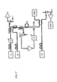
- FIG. 7 shows the experiment used to measure SIC and the linearizer circuit that compensates for the gain fluctuations.
- Optical signals L1, from a DFB laser with a wavelength of 1305 nm, and L2, from a gating-tuned external-cavity laser with a wavelength of 1290 nm, are amplified simultaneously.
- the traveling wave-amplifier has residual refectivities of 2 ⁇ 10 -4 , providing a fiber-to-fiber gain of 14 dB with a ⁇ 0.5 dB gain ripple.
- Fiber-to-fiber coupling losses including an optical isolator at the output, total 10 dB.
- High-speed InGaAs photodiodes PIN1 and PIN2 are used for direct detection of the intensity modulated L1 signal and for heterodyne detection of the output from the amplifier, respectively.
- a second external-cavity laser operated at a frequency within 2 GHz of L2, is used as a local oscillator.
- the linearizer uses the third photodiode PIN3 to sample the intensity of the signal at the input to the amplifier. The sampled signal is amplified by approximately 50 dB and used to modulate the amplifier bias.
- a fiber delay AL and a microwave variable phase shifter (not shown) are used to equalize the propagation delay for the detected electronic signal and the optical signal injected into the amplifier.
- the bandwidth of the feed-forward circuit is approximately 2 GHz.
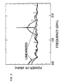
- Fig. 9 shows both the heterodyne-detected spectrum of the amplified L2 signal (centered at 1.5 GHz), when L1 is intensity modulated with 200-Mb/s pseudorandom data, and the direct-detected spectrum of L1 (frequencies less than 600 MHz). Since modulation was not applied to L2, the modulation evident in the amplified spectrum is the crosstalk induced by the amplification of L1. With the linearizer, the crosstalk is reduced by approximately 20 dB. Also, as evident from the 6-dB difference shown at zero frequency in FIG. 9, the effective gain of the amplifier is increased by 3 dB (optical).
Landscapes
- Physics & Mathematics (AREA)
- Condensed Matter Physics & Semiconductors (AREA)
- General Physics & Mathematics (AREA)
- Electromagnetism (AREA)
- Optics & Photonics (AREA)
- Engineering & Computer Science (AREA)
- Power Engineering (AREA)
- Optical Communication System (AREA)
Applications Claiming Priority (3)
| Application Number | Priority Date | Filing Date | Title |
|---|---|---|---|
| US22195288A | 1988-07-20 | 1988-07-20 | |
| US221952 | 1988-07-20 | ||
| SG22994A SG22994G (en) | 1988-07-20 | 1994-02-07 | Optical amplifier with reduced nonlinearity |
Publications (3)
| Publication Number | Publication Date |
|---|---|
| EP0352021A2 true EP0352021A2 (de) | 1990-01-24 |
| EP0352021A3 EP0352021A3 (en) | 1990-08-22 |
| EP0352021B1 EP0352021B1 (de) | 1993-10-06 |
Family
ID=26663879
Family Applications (1)
| Application Number | Title | Priority Date | Filing Date |
|---|---|---|---|
| EP89307109A Expired - Lifetime EP0352021B1 (de) | 1988-07-20 | 1989-07-13 | Optischer Verstärker mit reduzierter Nichtlinearität |
Country Status (5)
| Country | Link |
|---|---|
| EP (1) | EP0352021B1 (de) |
| JP (1) | JPH0267526A (de) |
| DE (1) | DE68909704T2 (de) |
| ES (1) | ES2044123T3 (de) |
| SG (1) | SG22994G (de) |
Cited By (4)
| Publication number | Priority date | Publication date | Assignee | Title |
|---|---|---|---|---|
| GB2282019A (en) * | 1993-09-20 | 1995-03-22 | Fujitsu Ltd | Optical amplifier |
| EP0762579A1 (de) * | 1995-08-29 | 1997-03-12 | AT&T Corp. | Optische Mehrfachfrequenzsignalquelle mit reduzierten Verzerrung und Übersprechen |
| US6417956B1 (en) * | 1996-09-26 | 2002-07-09 | Dsc Communications A/S | Method and an apparatus for amplitude equalization of a plurality of optical signals |
| EP1296447A4 (de) * | 2000-06-30 | 2005-08-03 | Mitsubishi Electric Corp | Hochfrequenzverstärker |
Families Citing this family (2)
| Publication number | Priority date | Publication date | Assignee | Title |
|---|---|---|---|---|
| KR19990035458A (ko) * | 1997-10-31 | 1999-05-15 | 윤종용 | 증폭이득 고정형 광증폭기 |
| JP6633470B2 (ja) * | 2016-07-28 | 2020-01-22 | 日本電信電話株式会社 | 光送信機、光受信機及び光送受信機 |
Family Cites Families (6)
| Publication number | Priority date | Publication date | Assignee | Title |
|---|---|---|---|---|
| JPS5482149A (en) * | 1977-12-14 | 1979-06-30 | Fujitsu Ltd | Microwave amplifier |
| JPS58125904A (ja) * | 1982-01-22 | 1983-07-27 | Mitsubishi Electric Corp | 零点補正回路 |
| JPS59101629A (ja) * | 1982-12-01 | 1984-06-12 | Nec Corp | ファイバ内光増幅装置 |
| CA1251845A (en) * | 1984-08-06 | 1989-03-28 | Ian D. Henning | Optical amplification |
| US4712075A (en) * | 1985-11-27 | 1987-12-08 | Polaroid Corporation | Optical amplifier |
| GB8611241D0 (en) * | 1986-05-08 | 1986-06-18 | British Telecomm | Optical amplifiers |
-
1989
- 1989-07-13 EP EP89307109A patent/EP0352021B1/de not_active Expired - Lifetime
- 1989-07-13 ES ES89307109T patent/ES2044123T3/es not_active Expired - Lifetime
- 1989-07-13 DE DE89307109T patent/DE68909704T2/de not_active Expired - Fee Related
- 1989-07-20 JP JP1186226A patent/JPH0267526A/ja active Pending
-
1994
- 1994-02-07 SG SG22994A patent/SG22994G/en unknown
Cited By (6)
| Publication number | Priority date | Publication date | Assignee | Title |
|---|---|---|---|---|
| GB2282019A (en) * | 1993-09-20 | 1995-03-22 | Fujitsu Ltd | Optical amplifier |
| US5479423A (en) * | 1993-09-20 | 1995-12-26 | Fujitsu Limited | Method of modulating feedback signal in optical amplifier to compensate for pump laser saturation |
| GB2282019B (en) * | 1993-09-20 | 1997-12-10 | Fujitsu Ltd | Methods of modulating feedback signals in optical amplifiers |
| EP0762579A1 (de) * | 1995-08-29 | 1997-03-12 | AT&T Corp. | Optische Mehrfachfrequenzsignalquelle mit reduzierten Verzerrung und Übersprechen |
| US6417956B1 (en) * | 1996-09-26 | 2002-07-09 | Dsc Communications A/S | Method and an apparatus for amplitude equalization of a plurality of optical signals |
| EP1296447A4 (de) * | 2000-06-30 | 2005-08-03 | Mitsubishi Electric Corp | Hochfrequenzverstärker |
Also Published As
| Publication number | Publication date |
|---|---|
| JPH0267526A (ja) | 1990-03-07 |
| ES2044123T3 (es) | 1994-01-01 |
| SG22994G (en) | 1995-03-17 |
| DE68909704T2 (de) | 1994-02-03 |
| EP0352021A3 (en) | 1990-08-22 |
| DE68909704D1 (de) | 1993-11-11 |
| EP0352021B1 (de) | 1993-10-06 |
Similar Documents
| Publication | Publication Date | Title |
|---|---|---|
| Yao | Brillouin selective sideband amplification of microwave photonic signals | |
| US5017885A (en) | Optical amplifier with reduced nonlinearity | |
| Olsson et al. | Characteristics of a semiconductor laser pumped Brillouin amplifier with electronically controlled bandwidth | |
| US6535328B2 (en) | Methods and devices based on brillouin selective sideband amplification | |
| US8103178B2 (en) | Linearized phase modulated analog optical links | |
| USRE43422E1 (en) | Tunable optical local oscillator | |
| US5287212A (en) | Optical link | |
| EP1079552A2 (de) | Verfahren , optische Vorrichtung und optisches System zur optischen Faserübertragung | |
| KR100368793B1 (ko) | 전광 nor 논리소자 구현장치 및 그 방법 | |
| JPS6113231A (ja) | 光信号増幅器及び光伝送システム | |
| EP0352021B1 (de) | Optischer Verstärker mit reduzierter Nichtlinearität | |
| CA1311039C (en) | Optical amplifier with reduced nonlinearity | |
| US7324256B1 (en) | Photonic oscillator | |
| Andersson et al. | Generation of BER floors from laser diode chirp noise | |
| Wilson et al. | Integrated electroabsorption modulator/DBR laser linearized by RF current modulation | |
| Udvary et al. | Semiconductor optical amplifiers in analog optical links | |
| US11163206B1 (en) | Active modulator with integrated LNA driver | |
| JPH0731314B2 (ja) | 光信号の変調装置 | |
| Veselka et al. | Optical soliton generator based on a single Mach-Zehnder modulator | |
| Lelièvre et al. | Photonics-based high purity microwave oscillators at 10 GHz | |
| Udvary et al. | Semiconductor optical amplifier for detection function in subcarrier multiplexed systems | |
| Udvary et al. | Noise and gain properties of semiconductor optical amplifiers | |
| Romisch et al. | Performance evaluation of optoelectronic oscillators | |
| Udvary et al. | Branching function by semiconductor optical amplifier (SOA) in subcarrier multiplexed (SCM) optical systems | |
| Lin et al. | Analog amplification by Raman scattering in optical fibers |
Legal Events
| Date | Code | Title | Description |
|---|---|---|---|
| PUAI | Public reference made under article 153(3) epc to a published international application that has entered the european phase |
Free format text: ORIGINAL CODE: 0009012 |
|
| AK | Designated contracting states |
Kind code of ref document: A2 Designated state(s): DE ES FR GB IT NL SE |
|
| PUAL | Search report despatched |
Free format text: ORIGINAL CODE: 0009013 |
|
| AK | Designated contracting states |
Kind code of ref document: A3 Designated state(s): DE ES FR GB IT NL SE |
|
| 17P | Request for examination filed |
Effective date: 19901211 |
|
| 17Q | First examination report despatched |
Effective date: 19920821 |
|
| GRAA | (expected) grant |
Free format text: ORIGINAL CODE: 0009210 |
|
| AK | Designated contracting states |
Kind code of ref document: B1 Designated state(s): DE ES FR GB IT NL SE |
|
| REF | Corresponds to: |
Ref document number: 68909704 Country of ref document: DE Date of ref document: 19931111 |
|
| ET | Fr: translation filed | ||
| ITF | It: translation for a ep patent filed | ||
| REG | Reference to a national code |
Ref country code: ES Ref legal event code: FG2A Ref document number: 2044123 Country of ref document: ES Kind code of ref document: T3 |
|
| RAP4 | Party data changed (patent owner data changed or rights of a patent transferred) |
Owner name: AT&T CORP. |
|
| PLBE | No opposition filed within time limit |
Free format text: ORIGINAL CODE: 0009261 |
|
| STAA | Information on the status of an ep patent application or granted ep patent |
Free format text: STATUS: NO OPPOSITION FILED WITHIN TIME LIMIT |
|
| 26N | No opposition filed | ||
| EAL | Se: european patent in force in sweden |
Ref document number: 89307109.2 |
|
| REG | Reference to a national code |
Ref country code: GB Ref legal event code: IF02 |
|
| PGFP | Annual fee paid to national office [announced via postgrant information from national office to epo] |
Ref country code: SE Payment date: 20020625 Year of fee payment: 14 |
|
| PGFP | Annual fee paid to national office [announced via postgrant information from national office to epo] |
Ref country code: ES Payment date: 20020710 Year of fee payment: 14 |
|
| PGFP | Annual fee paid to national office [announced via postgrant information from national office to epo] |
Ref country code: DE Payment date: 20020916 Year of fee payment: 14 |
|
| PG25 | Lapsed in a contracting state [announced via postgrant information from national office to epo] |
Ref country code: ES Free format text: LAPSE BECAUSE OF NON-PAYMENT OF DUE FEES Effective date: 20030714 Ref country code: SE Free format text: LAPSE BECAUSE OF NON-PAYMENT OF DUE FEES Effective date: 20030714 |
|
| PG25 | Lapsed in a contracting state [announced via postgrant information from national office to epo] |
Ref country code: DE Free format text: LAPSE BECAUSE OF NON-PAYMENT OF DUE FEES Effective date: 20040203 |
|
| EUG | Se: european patent has lapsed | ||
| REG | Reference to a national code |
Ref country code: ES Ref legal event code: FD2A Effective date: 20030714 |
|
| PG25 | Lapsed in a contracting state [announced via postgrant information from national office to epo] |
Ref country code: IT Free format text: LAPSE BECAUSE OF NON-PAYMENT OF DUE FEES Effective date: 20050713 |
|
| PGFP | Annual fee paid to national office [announced via postgrant information from national office to epo] |
Ref country code: NL Payment date: 20080716 Year of fee payment: 20 Ref country code: FR Payment date: 20080715 Year of fee payment: 20 |
|
| PGFP | Annual fee paid to national office [announced via postgrant information from national office to epo] |
Ref country code: GB Payment date: 20080722 Year of fee payment: 20 |
|
| REG | Reference to a national code |
Ref country code: GB Ref legal event code: PE20 Expiry date: 20090712 |
|
| NLV7 | Nl: ceased due to reaching the maximum lifetime of a patent |
Effective date: 20090713 |
|
| PG25 | Lapsed in a contracting state [announced via postgrant information from national office to epo] |
Ref country code: NL Free format text: LAPSE BECAUSE OF EXPIRATION OF PROTECTION Effective date: 20090713 Ref country code: GB Free format text: LAPSE BECAUSE OF EXPIRATION OF PROTECTION Effective date: 20090712 |