EP0352085B1 - Elektronenmikroskop - Google Patents
Elektronenmikroskop Download PDFInfo
- Publication number
- EP0352085B1 EP0352085B1 EP89307301A EP89307301A EP0352085B1 EP 0352085 B1 EP0352085 B1 EP 0352085B1 EP 89307301 A EP89307301 A EP 89307301A EP 89307301 A EP89307301 A EP 89307301A EP 0352085 B1 EP0352085 B1 EP 0352085B1
- Authority
- EP
- European Patent Office
- Prior art keywords
- electron
- casing
- chamber
- modules
- electron gun
- Prior art date
- Legal status (The legal status is an assumption and is not a legal conclusion. Google has not performed a legal analysis and makes no representation as to the accuracy of the status listed.)
- Expired - Lifetime
Links
- 238000010894 electron beam technology Methods 0.000 claims description 20
- 125000006850 spacer group Chemical group 0.000 claims description 8
- 238000011109 contamination Methods 0.000 description 5
- 238000010276 construction Methods 0.000 description 3
- 238000009792 diffusion process Methods 0.000 description 3
- XEEYBQQBJWHFJM-UHFFFAOYSA-N Iron Chemical compound [Fe] XEEYBQQBJWHFJM-UHFFFAOYSA-N 0.000 description 2
- 230000005540 biological transmission Effects 0.000 description 2
- 230000000694 effects Effects 0.000 description 2
- 239000000696 magnetic material Substances 0.000 description 2
- 239000000463 material Substances 0.000 description 2
- 229910000851 Alloy steel Inorganic materials 0.000 description 1
- ATJFFYVFTNAWJD-UHFFFAOYSA-N Tin Chemical compound [Sn] ATJFFYVFTNAWJD-UHFFFAOYSA-N 0.000 description 1
- 238000004891 communication Methods 0.000 description 1
- 230000001010 compromised effect Effects 0.000 description 1
- 238000013016 damping Methods 0.000 description 1
- 238000013461 design Methods 0.000 description 1
- 238000001514 detection method Methods 0.000 description 1
- 229910052742 iron Inorganic materials 0.000 description 1
- 230000003287 optical effect Effects 0.000 description 1
- 229910000889 permalloy Inorganic materials 0.000 description 1
- 230000000630 rising effect Effects 0.000 description 1
- 238000007789 sealing Methods 0.000 description 1
- 238000010561 standard procedure Methods 0.000 description 1
- 239000010959 steel Substances 0.000 description 1
- 238000012546 transfer Methods 0.000 description 1
Images


Classifications
-
- H—ELECTRICITY
- H01—ELECTRIC ELEMENTS
- H01J—ELECTRIC DISCHARGE TUBES OR DISCHARGE LAMPS
- H01J37/00—Discharge tubes with provision for introducing objects or material to be exposed to the discharge, e.g. for the purpose of examination or processing thereof
- H01J37/02—Details
- H01J37/18—Vacuum locks ; Means for obtaining or maintaining the desired pressure within the vessel
-
- H—ELECTRICITY
- H01—ELECTRIC ELEMENTS
- H01J—ELECTRIC DISCHARGE TUBES OR DISCHARGE LAMPS
- H01J37/00—Discharge tubes with provision for introducing objects or material to be exposed to the discharge, e.g. for the purpose of examination or processing thereof
- H01J37/02—Details
- H01J37/16—Vessels; Containers
Definitions
- the present invention relates to an electron microscope, e.g. a scanning electron microscope or a transmission electron microscope.
- An electron microscope normally consists of a specimen chamber in which the specimen to be analysed is located, and an electron column which generates a beam of electrons which are used to bombard the specimen.
- That electron column itself normally has two parts, an electron gun chamber containing an electron gun for generating the beam of electrons, and a casing containing an electron lens arrangement.
- That electron lens arrangement usually includes a plurality of condenser lenses arranged vertically inside the casing with the electron beam passing down a central axis of those condenser lenses.
- Alignment coils for aligning the electrons into a narrow beam are located between the condenser and the electron gun.
- scanning coils deflection coils
- an electron beam path is defined between the electron gun and the sample, passing through the lenses and coils.
- the sample chamber must also be evacuated.
- the standard method of evacuating the interior of the electron column is to connect that column to a vacuum pump via a plurality of ducts which extend from the vacuum pump through the walls of the electron column.
- Example of such an arrangement is shown in Japanese patent application number JP-A- 49-131376, in which there are three ducts extending from the electron column and one from the sample chamber which are interconnected at a diffusion pump.
- JP-A- 55-136446 there are again a plurality of ducts leading from the electron column.
- the presence of such ducts causes a number of problems.
- the first problem is that, if a good vacuum is to be achieved within the electron column, it is necessary that the ducts be relatively large, so that they have satisfactory conductance.
- the size of the ducts is inconvenient, and limits the positioning of additional devices which may be needed around the electron column, such as an X-ray system.
- a further problem associated with the presence of the ducts to the vacuum pump is that their presence means that apertures must be made in any magnetic shielding around the electron column. Stray magnetic fields may cause magnetic disturbance, and if this is allowed to affect the electron beam, the accuracy of the operation of the microscope may be compromised. For example, a magnetic disturbance due to e.g. mains noise may cause a ripple on the image produced by the electron microscope, thereby blurring that image. Therefore, in order to limit magnetic disturbance, it is known to place a shielding cylinder around the electron column, but it is necessary that apertures be made in that shielding to permit the ducting to the vacuum pump to emerge. Bearing in mind that that ducting needs to be large in order to achieve a good vacuum, there is thus a conflict between the need for a good vacuum and the need for good magnetic shielding.
- GB-A-1213374 discloses an electron microscope in which the above arrangements are modified so the evacuation ducts are formed by bores in the wall of the casing. There is a vertical bore extending the length of the casing, and that vertical bore is connected to the interior of the casing containing the electron lenses by lateral bores.
- an electron microscope having a hollow sample changer, a casing mounted on the sample chamber and containing an electron lens system, and an electron gun chamber mounted on the casing with an electron beam path being defined between the electron gas chamber and the sample chamber through the lens system;
- the electron lens system comprises a plurality of sealed modules, each of the sealed modules containing an electron lens, and having a bore therethrough for defining part of the electron beam path, an evacuation path being defined in the casing from the sample chamber to the electron gun chamber around the sealed modules, at least part of that path being defined between an outer wall of each module and an inner wall of the casing.
- an electron beam column for an electron microscope comprising: a hollow casing; a plurality of modules within said casing, each of said modules having at least one electron lens sealed therein, and a hollow electron gun chamber secured to one end said casing; there being at least one evacuation hole extending between the interior of the electron gun chamber and the interior of the casing and at least part of an outer wall of each said module being spaced from the interior wall of the casing, to define part of an evacuation path around each such module, whereby the evacuation path extends from said electron gun chamber, through said holes and around said modules, to the end of said casing remote from said electron gun chamber.
- the casing containing the electron lens assembly may be made from a closed enclosure, together with the electron gun chamber and the sample chamber. Then by connecting suitable evacuation means in the form of e.g. a vacuum pump to the sample changer, the whole interior can be evacuated.
- suitable evacuation means in the form of e.g. a vacuum pump to the sample changer, the whole interior can be evacuated.
- the magnetic shielding since the ducting outside the electron column is dispensed with, it becomes possible for the magnetic shielding to be unbroken, except possibly where the electron microscope has an adjustable aperture (which is normally positioned between the condenser lenses and the deflection coils) since the control for that adjustable aperture has to project through the magnetic shielding.
- the magnetic shielding may simply extend along the casing, and be sealed to the outside of the sample chamber, but preferably there is a further shielding part which encloses the electron gun chamber.
- the evacuation path is defined within the casing, its size needs to be sufficiently large to permit a high conductance.
- suitable apertures between the electron gun chamber and the casing, adjacent the condenser lenses, and between the casing and the sample chamber permit a sufficiently high conductance to be achieved. Indeed, it is possible with the present invention to achieve a higher conductance than was normally achieved in standard arrangements using external ducting.
- Japanese patent application number JP-A- 59-209045 apparently shows an arrrangement in which there is no external ducting.
- the device shown in that disclosure is an electron analysing apparatus which involves the detection of Auger electrons, and therefore must operate under extremely high vacuum, much higher than is normally used in electron microscopes such as scanning electron microscopes or transmission electron microscopes. Therefore, a skilled man reading Japanese patent application number JP-A- 59-209045 will immediately appreciate that what is illustrated is wholly schematic, and that additional ducting would be necessary in order to achieve the desired level of vacuum. Indeed, this can be seen from the fact that the arrangement is illustrated with the condenser lenses apparently directly contacting the vacuum, which would result in contamination and would not operate satisfactorily.
- the electron lenses should be sealed from the vacuum.
- those electron lenses are mounted in sealed modules, and a plurality of such modules positioned within the casing of the electron.
- a bore extends through the centre of those modules, to define the electron beam path, but by suitable design of the modules, the evacuation path may be between the outer wall of those modules and the inner wall of the casing.
- the modules may be spaced by suitable spacers. It is desirable that those spacers have apertures therein so that they may thus form part of the evacuation path.
- the main limit on conductance from the electron gun chamber to the specimen chamber is at the mounting of the electron gun chamber to the casing, and the mounting of the casing to the specimen chamber.
- a plurality of apertures are usually necessary, and, particularly between the electron gun chamber and the casing, this may be achieved by providing a tie member in the form of a plate with a plurality of apertures therein.
- a scanning electron microscope comprises an electron column 10 (which will be described in more detail later) mounted on a specimen chamber 12. That specimen chamber is hollow, and a specimen support 14 extends into that hollow specimen chamber 12 for supporting a specimen 16 below the electron column.
- Figure 1 also shows an enclosure 18 for magnetic shielding, from which extends a power cable 20 for powering the electron gun of the electron column.
- the specimen chamber is mounted on a stage 22 which is supported via damping supports 24 on a frame 26.
- Figure 1 also illustrates the vacuum system for evacuating the specimen chamber 12.
- the duct 28 extends from that specimen chamber 12 and a first branch 30 extends via a valve 32 to a diffusion pump 40 which is itself connected via a valve 42 to the rotary pump 34.
- valves 38 and 42 are first closed, and the rotary pump operated to reduce the pressure within the specimen chamber 12.
- the valve 32 is closed and the valves 38 and 42 opened.
- the diffusion pump 40 continues the evacuation of the specimen chamber 12 until a suitable vacuum has been achieved.
- vacuum systems may be used, however, such as e.g. a turbo-molecular pump.
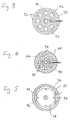
- FIG. 2 shows the structure of the electron column in more detail, it can be seen that that comlumn comprises a plurality of parts.
- the electron gun chamber comprises an upper part 46 and a lower part 48 sealed together, the lower part being connected to a casing 50 for electron lenses via a spacer plate 52.
- the alignment coil assembly 54 which, as can be seen, has a bore 57 therein which forms part of the path of the electron beam. Although not illustrated, that bore 57 will normally contain a lining having only a small aperture therein to collimate the beam. It should be noted, that tin order to prevent contamination, the alignment coil assembly 54 is hermetically sealed from the interior of the electron gun chamber 42 and the interior of the casing 50.
- the casing 50 contains a plurality of modules 56 58 containing condenser electron lenses.
- Figure 2 shows two such modules 56, 58, but more may be provided if necessary.
- Module 56 is shown in sectional view, and it can be seen there that the coils 60 of the lens are encased within magnetic shielding material formed by two shielding parts 62, 64.
- Power cables 66 extend from each module out of the casing, 50 and are connected to a suitable power supply.
- Bores 68 extend down the centre of the modules to form the electron beam path, and these bores 68 may contain collimating apertures.
- Module 56 is shown in sectional view, and it can be seen there that the coils 60 of the lensare encases within magnetic shielding material formed by two shielding parts 62, 64.
- Power cables 66 extend from each module out of the casing, 50 and are connected to a suitable power supply.
- Bores 68 extend down the centre of the modules to form the electron beam path.
- each module 56, 58 is not sealed to the walls of the casing 50, but may simply be fitted therein provided that a close tolerance is achieved. It can be seen in figure 2, each module has a flange 70 thereon which fits against the wall of the casing, with the rest of the module 56, 58 being of smaller diameter than the interior of the casing 50.
- the modules 56, 58 themselves are separated by a spacer 72, having openings 74 therein, and a further spacer 76 may be provided, again having holes therein, between the upper module 58, and the tie plate 52.
- the casing 50 is connected via a further tie plate 78 to the specimen chamber 12.
- a spacer block 80 of non-magnetic material may be provided between that tie block 78 and the specimen chamber 12, with rings 82, 84 sealing the tie block 78 to the spacer 80 and the casing 50 respectively.
- a deflection coil unit 86 again having a bore therein to define the electron beam path, and attached to the bottom of the tie block 78 is an objective lens assembly 87.
- the resulting assembly is enclosed within the enclosure 18 for magnetic shielding, which enclosure comprises a lower shielding member 88 and an upper shielding member 90.
- the lower shielding member 88 is sealed to the outside of the specimen chamber 12, and extends to cover the tie block 78, the casing 50, and the lower part 48 of the electron gun chamber. It is this region which is most susceptible to magnetic disturbance.
- a further magnetic shield 90 be provided covereing the top of the electron gun chamber.
- this magnetic shielding be as continuous as possible, to prevent magnetic distrubance of the electron beam, and it can be seen from Figure 2 that the shielding is substantially continuous from the specimen chamber 12 to the electron gun chamber 42, and indeed may cover that chamber completely.
- control 92 of an adjustable aperture device which is located in the electron beam path. Since such a device is optional, the control 92 may be omitted in some cases in which case the shielding may then be completely continuous.
- an evacuation path to permit evacuation of the interior of the electron column is provided within the casing 50, so that no ducting passes through the enclosure formed by the magnetic shield. This evacuation path will now be described in more detail.
- the tie plate 78 has a plurality of bores 92 therein, thereby linking the interior of the casing 50 with the interior of the specimen chamber 12. Furthermore, the flange 70 of each lens module 56, 58, is cut, as can be seen for the lens module 56 in Figure 5.
- Figure 5 illustrates two cut-away parts 94, but in actuality, at least one cut-away is needed in form. That is, it is necessary to employ a construction which makes it possible to allow the condenser lens module 50 to fit the inside of the jacket casing 50 and to keep an evacuation space therebetween.
- cut-away parts 94 and the spacings 96 between the walls of the electron lens modules 56, 58 and the internal wall of the casing 50 permit a flow path around those modules 56, 58.
- the plate 52 and the adjacent part of the lower part 48 of the electron gun chamber are provided with through bores 99 as shown in Fig. 4.
- the evacuation path is defined from the sample chamber 12 to the interior of the electron gun chamber 42 through bores 92, cut-away parts 94, spacings 96 and bores 99.
- the conductance C4 per hole is 12.4l/s obtained by the same operation as above.
- the conductance given by two openings as illustrated is 328l/s.
- the conductance C of the electron gun chamber can be computed from the above equation (2), but since the conductance given by the two openings 94 is far larger than that given by the holes 92, 98 the conductance C of the electron gun chamber may be neglected when computing the conductance of this embodiment as follows:
- the electron gun chamber and the electon beam path can be kent in a high vacuum state as well as suppressing contamination in the overall system.
- this embodiment needs no opening for a pipeline on a shielding cylinder 88 if the electron microscope is covered by the shielding cylinder 88 for improving the magnetic shielding.
- more magnetic shielding and easier mounting and dismounting of the shielding cylinder may be achieved than in the prior art.
- a magnetic material such as pure iron, soft steel, or Permalloy for the tie block and the casing.
- the coils are hematically isolated from the vacuum and a high conductance is achieved for communication between the specimen chamber 12, the interior of the casing, the electron beam path, and the electron gun chamber. It is therefore possible to suppress contamination in the path where the electron beam passes and to keep the space at high vacuum.
Landscapes
- Chemical & Material Sciences (AREA)
- Analytical Chemistry (AREA)
- Analysing Materials By The Use Of Radiation (AREA)
- Electron Sources, Ion Sources (AREA)
Claims (8)
- Elektronenmikroskop mit einer hohlen Probenkammer (12), einem an der Probenkammer (12) angebrachten Mantel (50), der ein Elektronenlinsensystem (56, 58) enthält, und einer Elektronenkanonenkammer (43), die am Mantel (50) angebracht ist, mit einem Elektronenstrahlweg, der zwischen der Elektronenkanonenkammer (43) und der Probenkammer (12) durch das Linsensystem (50, 58) hindurch festgelegt ist;
dadurch gekennzeichnet, daß:
- das Elektronenlinsensystem (56, 58) mehrere abgedichtete Module aufweist, wobei jedes der abgedichteten Module eine Elekronenlinse enthält und über eine durchgehende Bohrung verfügt, um einen Teil des Elektronenstrahlwegs festzulegen, wobei ein Abpumppfad im Mantel von der Probenkammer (12) zur Elektronenkanonenkammer (43) um die abgedichteten Module herum festgelegt ist, wobei mindestens ein Teil dieses Pfads zwischen der Außenwand jedes Moduls und der Innenwand des Mantels (50) festgelegt ist. - Elektronenmikroskop nach Anspruch 1, mit einer Abstandshalterplatte (72, 76) zwischen jedem der Module, mit einer Öffnung (74) darin, die einen Teil des Abpumppfads bildet.
- Elektronenmikroskop nach Anspruch 2, mit einem ersten Verbindungsteil (52) zwischen der Elektronenkanonenkammer (43) und dem Mantel (50), mit mehreren darin angeordneten Löchern (99), die einen Teil des Abpumppfads festlegen.
- Elektronenmikroskop nach einem der vorstehenden Ansprüche, mit einem zweiten Verbindungsteil (78) zwischen dem Mantel (50) und der Probenkammer (12), mit einer Mehrzahl darin enthaltener Löcher (92), die einen Teil des Evakuierpfads festlegen.
- Elektronenmikroskop nach einem der vorstehenden Ansprüche mit einer magnetisch abschirmenden Außenhülle (18), die den Mantel (50) umgibt.
- Elektronenmikroskop in Anspruch 5, bei dem die magnetisch abschirmende Außenhülle (18) gegen die Probenkammer (12) abgedichtet ist.
- Elektronenmikroskop nach Anspruch 5 oder Anspruch 6, bei dem die Abschirmung (18) auch die Elektronenkanonenkammer (42) umgibt.
- Elektronenstrahlsäule für ein Elektronenmikroskop, mit:- einem hohlen Mantel (50);- mehreren Modulen innerhalb dieses Mantels, wobei jeder Modul mindestens eine abgedichtete in ihm angeordnete Elektronenlinse aufweist; und- einer hohlen Elektronenkanonenkammer (43), die an einem Ende des Mantels befestigt ist;- wobei sich mindestens ein Abpumploch (99) zwischen dem Innenraum der Elektronenkanonenkammer (43) und dem Innenraum des Mantels (50) erstreckt und mindestens ein Teil der Außenwand des Moduls von der Innenwand des Mantels beabstandet ist, um einen Teil eines Evakuierpfads um jeden solchen Modul herum festzulegen, wobei sich der Abpumppfad von der Elektronenkanonenkammer (43) aus durch die Löcher und um die Module herum zum Ende des Mantels (50) erstreckt, das von der Elektronenkanonenkammer (43) entfernt liegt.
Applications Claiming Priority (2)
| Application Number | Priority Date | Filing Date | Title |
|---|---|---|---|
| JP182991/88 | 1988-07-22 | ||
| JP63182991A JPH0760661B2 (ja) | 1988-07-22 | 1988-07-22 | 電子顕微鏡 |
Publications (3)
| Publication Number | Publication Date |
|---|---|
| EP0352085A2 EP0352085A2 (de) | 1990-01-24 |
| EP0352085A3 EP0352085A3 (en) | 1990-11-28 |
| EP0352085B1 true EP0352085B1 (de) | 1994-10-26 |
Family
ID=16127843
Family Applications (1)
| Application Number | Title | Priority Date | Filing Date |
|---|---|---|---|
| EP89307301A Expired - Lifetime EP0352085B1 (de) | 1988-07-22 | 1989-07-19 | Elektronenmikroskop |
Country Status (4)
| Country | Link |
|---|---|
| US (1) | US5029249A (de) |
| EP (1) | EP0352085B1 (de) |
| JP (1) | JPH0760661B2 (de) |
| DE (1) | DE68919004T2 (de) |
Families Citing this family (10)
| Publication number | Priority date | Publication date | Assignee | Title |
|---|---|---|---|---|
| JPH0756443B2 (ja) * | 1990-12-20 | 1995-06-14 | 株式会社島津製作所 | 生体試料観察用走査型トンネル顕微鏡 |
| US5748866A (en) * | 1994-06-30 | 1998-05-05 | International Business Machines Corporation | Virtual display adapters using a digital signal processing to reformat different virtual displays into a common format and display |
| SG74599A1 (en) * | 1997-09-27 | 2000-08-22 | Inst Of Material Res & Enginee | Portable high resolution scanning electron microscope column using permanent magnet electron lenses |
| US6297512B1 (en) * | 1998-03-31 | 2001-10-02 | Cirrus Logic, Inc. | Double shield for electron and ion beam columns |
| JP3117950B2 (ja) * | 1998-05-21 | 2000-12-18 | セイコーインスツルメンツ株式会社 | 荷電粒子装置 |
| US6515282B1 (en) * | 2000-03-28 | 2003-02-04 | Applied Materials, Inc. | Testing of interconnection circuitry using two modulated charged particle beams |
| US20020148971A1 (en) * | 2001-03-05 | 2002-10-17 | Michael Sogard | Lens assembly for electron beam column |
| JP4621097B2 (ja) * | 2005-09-14 | 2011-01-26 | 株式会社日立ハイテクノロジーズ | 電子線装置およびその制御方法 |
| DE602007007468D1 (de) | 2007-07-27 | 2010-08-12 | Integrated Circuit Testing | Magnetische Linsenanordnung |
| CN102163529B (zh) * | 2011-03-15 | 2012-07-25 | 北京航空航天大学 | 电子显微镜的聚光镜用可动光阑装置 |
Family Cites Families (15)
| Publication number | Priority date | Publication date | Assignee | Title |
|---|---|---|---|---|
| US2637000A (en) * | 1951-02-15 | 1953-04-28 | Magnetic electron -lens | |
| US3346736A (en) * | 1964-09-22 | 1967-10-10 | Applied Res Lab Inc | Electron probe apparatus having an objective lens with an aperture for restricting fluid flow |
| US3535515A (en) * | 1967-06-14 | 1970-10-20 | Us Navy | Ultrasonic apparatus for electron microscope |
| DE1804199C3 (de) * | 1968-03-26 | 1975-12-18 | Siemens Ag, 1000 Berlin Und 8000 Muenchen | Korpuskularstrahlgerät zur wahlweisen Abbildung eines Präparates oder seines Beugungsdiagrammes |
| GB1213374A (en) * | 1968-10-15 | 1970-11-25 | Ass Elect Ind | Improvements in or relating to electron optical systems |
| DE2307822C3 (de) * | 1973-02-16 | 1982-03-18 | Siemens AG, 1000 Berlin und 8000 München | Supraleitendes Linsensystem für Korpuskularstrahlung |
| JPS5344786B2 (de) * | 1975-03-26 | 1978-12-01 | ||
| DE3423149A1 (de) * | 1984-06-22 | 1986-01-02 | Fa. Carl Zeiss, 7920 Heidenheim | Verfahren und anordnung zur elektronenenergiegefilterten abbildung eines objektes oder eines objektbeugungsdiagrammes mit einem transmissions-elektronenmikroskop |
| NL8402340A (nl) * | 1984-07-25 | 1986-02-17 | Philips Nv | Microscoop voor niet-gedifferentieerde fase-beeldvorming. |
| JPS61138441A (ja) * | 1984-11-29 | 1986-06-25 | Fuji Photo Film Co Ltd | 電子顕微鏡像記録再生方法 |
| JPH0616386B2 (ja) * | 1986-01-10 | 1994-03-02 | 株式会社日立製作所 | 粒子線装置の絞りの清浄化法および装置 |
| JPS62260335A (ja) * | 1986-05-06 | 1987-11-12 | Hitachi Ltd | パタ−ン検査方法および装置 |
| GB2192092A (en) * | 1986-06-25 | 1987-12-31 | Philips Electronic Associated | Magnetic lens system |
| JPS6322062U (de) * | 1986-07-26 | 1988-02-13 | ||
| US4823006A (en) * | 1987-05-21 | 1989-04-18 | Electroscan Corporation | Integrated electron optical/differential pumping/imaging signal detection system for an environmental scanning electron microscope |
-
1988
- 1988-07-22 JP JP63182991A patent/JPH0760661B2/ja not_active Expired - Lifetime
-
1989
- 1989-07-18 US US07/381,191 patent/US5029249A/en not_active Expired - Fee Related
- 1989-07-19 EP EP89307301A patent/EP0352085B1/de not_active Expired - Lifetime
- 1989-07-19 DE DE68919004T patent/DE68919004T2/de not_active Expired - Fee Related
Also Published As
| Publication number | Publication date |
|---|---|
| DE68919004D1 (de) | 1994-12-01 |
| EP0352085A2 (de) | 1990-01-24 |
| US5029249A (en) | 1991-07-02 |
| EP0352085A3 (en) | 1990-11-28 |
| DE68919004T2 (de) | 1995-03-16 |
| JPH0233844A (ja) | 1990-02-05 |
| JPH0760661B2 (ja) | 1995-06-28 |
Similar Documents
| Publication | Publication Date | Title |
|---|---|---|
| EP0352085B1 (de) | Elektronenmikroskop | |
| US5036290A (en) | Synchrotron radiation generation apparatus | |
| US4066905A (en) | Particle beam apparatus with zones of different pressure | |
| JPH01309243A (ja) | 環境走査電子顕微鏡の対物レンズ組立体 | |
| US5177361A (en) | Electron energy filter | |
| US6590207B2 (en) | Microscale mass spectrometric chemical-gas sensor | |
| US5021702A (en) | Electron beam apparatus including a plurality of ion pump blocks | |
| US4458151A (en) | Electron microscope of a scanning type | |
| JPH1116525A (ja) | X線コンピュータトモグラフ装置 | |
| US6185279B1 (en) | Casing for electromagnetic radiation source and method for eliminating extrafocal electromagnetic radiation | |
| US4562352A (en) | Analyzing apparatus capable of analyzing a surface at a high resolution | |
| US20040144922A1 (en) | Electron microscope | |
| CA2163285C (en) | Means for reducing the contamination of mass spectrometer leak detector ion sources | |
| US20020153495A1 (en) | Magnetically shielded enclosures for housing charged-particle-beam systems | |
| US4616157A (en) | Injector for negative ions | |
| US4712012A (en) | Charge conversion unit for negative ion source | |
| US4931744A (en) | Synchrotron radiation source and method of making the same | |
| JP3501036B2 (ja) | 質量分析計 | |
| EP4364179B1 (de) | Multimodales niederspannungs-elektronenmikroskop | |
| CN120089589B (zh) | 一种电子电离型质谱仪前级系统 | |
| JPS583585B2 (ja) | 電子顕徴鏡等の試料室 | |
| US3800152A (en) | Electron analysis apparatus with heat-protective shield means spacedly overlying a sample supporting surface | |
| JP3367206B2 (ja) | イオン注入装置用の高電圧ボックス | |
| JPS643171Y2 (de) | ||
| JP2893742B2 (ja) | 電子線装置 |
Legal Events
| Date | Code | Title | Description |
|---|---|---|---|
| PUAI | Public reference made under article 153(3) epc to a published international application that has entered the european phase |
Free format text: ORIGINAL CODE: 0009012 |
|
| 17P | Request for examination filed |
Effective date: 19890906 |
|
| AK | Designated contracting states |
Kind code of ref document: A2 Designated state(s): DE GB |
|
| PUAL | Search report despatched |
Free format text: ORIGINAL CODE: 0009013 |
|
| AK | Designated contracting states |
Kind code of ref document: A3 Designated state(s): DE GB |
|
| 17Q | First examination report despatched |
Effective date: 19930406 |
|
| GRAA | (expected) grant |
Free format text: ORIGINAL CODE: 0009210 |
|
| AK | Designated contracting states |
Kind code of ref document: B1 Designated state(s): DE GB |
|
| REF | Corresponds to: |
Ref document number: 68919004 Country of ref document: DE Date of ref document: 19941201 |
|
| PLBE | No opposition filed within time limit |
Free format text: ORIGINAL CODE: 0009261 |
|
| STAA | Information on the status of an ep patent application or granted ep patent |
Free format text: STATUS: NO OPPOSITION FILED WITHIN TIME LIMIT |
|
| 26N | No opposition filed | ||
| PGFP | Annual fee paid to national office [announced via postgrant information from national office to epo] |
Ref country code: DE Payment date: 19990930 Year of fee payment: 11 |
|
| PG25 | Lapsed in a contracting state [announced via postgrant information from national office to epo] |
Ref country code: DE Free format text: LAPSE BECAUSE OF NON-PAYMENT OF DUE FEES Effective date: 20010501 |
|
| REG | Reference to a national code |
Ref country code: GB Ref legal event code: IF02 |
|
| PGFP | Annual fee paid to national office [announced via postgrant information from national office to epo] |
Ref country code: GB Payment date: 20060727 Year of fee payment: 18 |
|
| GBPC | Gb: european patent ceased through non-payment of renewal fee |
Effective date: 20070719 |
|
| PG25 | Lapsed in a contracting state [announced via postgrant information from national office to epo] |
Ref country code: GB Free format text: LAPSE BECAUSE OF NON-PAYMENT OF DUE FEES Effective date: 20070719 |