EP0352471B1 - Procédé de planariser de dispositifs semiconducteurs - Google Patents
Procédé de planariser de dispositifs semiconducteurs Download PDFInfo
- Publication number
- EP0352471B1 EP0352471B1 EP89111209A EP89111209A EP0352471B1 EP 0352471 B1 EP0352471 B1 EP 0352471B1 EP 89111209 A EP89111209 A EP 89111209A EP 89111209 A EP89111209 A EP 89111209A EP 0352471 B1 EP0352471 B1 EP 0352471B1
- Authority
- EP
- European Patent Office
- Prior art keywords
- layer
- semiconductor material
- gaas
- mask
- recess
- Prior art date
- Legal status (The legal status is an assumption and is not a legal conclusion. Google has not performed a legal analysis and makes no representation as to the accuracy of the status listed.)
- Expired - Lifetime
Links
Images



Classifications
-
- H—ELECTRICITY
- H10—SEMICONDUCTOR DEVICES; ELECTRIC SOLID-STATE DEVICES NOT OTHERWISE PROVIDED FOR
- H10P—GENERIC PROCESSES OR APPARATUS FOR THE MANUFACTURE OR TREATMENT OF DEVICES COVERED BY CLASS H10
- H10P10/00—Bonding of wafers, substrates or parts of devices
-
- H—ELECTRICITY
- H10—SEMICONDUCTOR DEVICES; ELECTRIC SOLID-STATE DEVICES NOT OTHERWISE PROVIDED FOR
- H10P—GENERIC PROCESSES OR APPARATUS FOR THE MANUFACTURE OR TREATMENT OF DEVICES COVERED BY CLASS H10
- H10P14/00—Formation of materials, e.g. in the shape of layers or pillars
- H10P14/20—Formation of materials, e.g. in the shape of layers or pillars of semiconductor materials
- H10P14/38—Formation of materials, e.g. in the shape of layers or pillars of semiconductor materials characterised by treatments done after the formation of the materials
-
- H—ELECTRICITY
- H10—SEMICONDUCTOR DEVICES; ELECTRIC SOLID-STATE DEVICES NOT OTHERWISE PROVIDED FOR
- H10P—GENERIC PROCESSES OR APPARATUS FOR THE MANUFACTURE OR TREATMENT OF DEVICES COVERED BY CLASS H10
- H10P14/00—Formation of materials, e.g. in the shape of layers or pillars
- H10P14/20—Formation of materials, e.g. in the shape of layers or pillars of semiconductor materials
- H10P14/27—Formation of materials, e.g. in the shape of layers or pillars of semiconductor materials using selective deposition, e.g. simultaneous growth of monocrystalline and non-monocrystalline semiconductor materials
-
- H—ELECTRICITY
- H10—SEMICONDUCTOR DEVICES; ELECTRIC SOLID-STATE DEVICES NOT OTHERWISE PROVIDED FOR
- H10P—GENERIC PROCESSES OR APPARATUS FOR THE MANUFACTURE OR TREATMENT OF DEVICES COVERED BY CLASS H10
- H10P14/00—Formation of materials, e.g. in the shape of layers or pillars
- H10P14/20—Formation of materials, e.g. in the shape of layers or pillars of semiconductor materials
- H10P14/29—Formation of materials, e.g. in the shape of layers or pillars of semiconductor materials characterised by the substrates
- H10P14/2901—Materials
- H10P14/2902—Materials being Group IVA materials
- H10P14/2905—Silicon, silicon germanium or germanium
-
- H—ELECTRICITY
- H10—SEMICONDUCTOR DEVICES; ELECTRIC SOLID-STATE DEVICES NOT OTHERWISE PROVIDED FOR
- H10P—GENERIC PROCESSES OR APPARATUS FOR THE MANUFACTURE OR TREATMENT OF DEVICES COVERED BY CLASS H10
- H10P14/00—Formation of materials, e.g. in the shape of layers or pillars
- H10P14/20—Formation of materials, e.g. in the shape of layers or pillars of semiconductor materials
- H10P14/29—Formation of materials, e.g. in the shape of layers or pillars of semiconductor materials characterised by the substrates
- H10P14/2924—Structures
- H10P14/2925—Surface structures
-
- H—ELECTRICITY
- H10—SEMICONDUCTOR DEVICES; ELECTRIC SOLID-STATE DEVICES NOT OTHERWISE PROVIDED FOR
- H10P—GENERIC PROCESSES OR APPARATUS FOR THE MANUFACTURE OR TREATMENT OF DEVICES COVERED BY CLASS H10
- H10P14/00—Formation of materials, e.g. in the shape of layers or pillars
- H10P14/20—Formation of materials, e.g. in the shape of layers or pillars of semiconductor materials
- H10P14/34—Deposited materials, e.g. layers
- H10P14/3402—Deposited materials, e.g. layers characterised by the chemical composition
- H10P14/3414—Deposited materials, e.g. layers characterised by the chemical composition being group IIIA-VIA materials
- H10P14/3421—Arsenides
-
- Y—GENERAL TAGGING OF NEW TECHNOLOGICAL DEVELOPMENTS; GENERAL TAGGING OF CROSS-SECTIONAL TECHNOLOGIES SPANNING OVER SEVERAL SECTIONS OF THE IPC; TECHNICAL SUBJECTS COVERED BY FORMER USPC CROSS-REFERENCE ART COLLECTIONS [XRACs] AND DIGESTS
- Y10—TECHNICAL SUBJECTS COVERED BY FORMER USPC
- Y10S—TECHNICAL SUBJECTS COVERED BY FORMER USPC CROSS-REFERENCE ART COLLECTIONS [XRACs] AND DIGESTS
- Y10S148/00—Metal treatment
- Y10S148/026—Deposition thru hole in mask
-
- Y—GENERAL TAGGING OF NEW TECHNOLOGICAL DEVELOPMENTS; GENERAL TAGGING OF CROSS-SECTIONAL TECHNOLOGIES SPANNING OVER SEVERAL SECTIONS OF THE IPC; TECHNICAL SUBJECTS COVERED BY FORMER USPC CROSS-REFERENCE ART COLLECTIONS [XRACs] AND DIGESTS
- Y10—TECHNICAL SUBJECTS COVERED BY FORMER USPC
- Y10S—TECHNICAL SUBJECTS COVERED BY FORMER USPC CROSS-REFERENCE ART COLLECTIONS [XRACs] AND DIGESTS
- Y10S148/00—Metal treatment
- Y10S148/072—Heterojunctions
-
- Y—GENERAL TAGGING OF NEW TECHNOLOGICAL DEVELOPMENTS; GENERAL TAGGING OF CROSS-SECTIONAL TECHNOLOGIES SPANNING OVER SEVERAL SECTIONS OF THE IPC; TECHNICAL SUBJECTS COVERED BY FORMER USPC CROSS-REFERENCE ART COLLECTIONS [XRACs] AND DIGESTS
- Y10—TECHNICAL SUBJECTS COVERED BY FORMER USPC
- Y10S—TECHNICAL SUBJECTS COVERED BY FORMER USPC CROSS-REFERENCE ART COLLECTIONS [XRACs] AND DIGESTS
- Y10S148/00—Metal treatment
- Y10S148/10—Lift-off masking
-
- Y—GENERAL TAGGING OF NEW TECHNOLOGICAL DEVELOPMENTS; GENERAL TAGGING OF CROSS-SECTIONAL TECHNOLOGIES SPANNING OVER SEVERAL SECTIONS OF THE IPC; TECHNICAL SUBJECTS COVERED BY FORMER USPC CROSS-REFERENCE ART COLLECTIONS [XRACs] AND DIGESTS
- Y10—TECHNICAL SUBJECTS COVERED BY FORMER USPC
- Y10S—TECHNICAL SUBJECTS COVERED BY FORMER USPC CROSS-REFERENCE ART COLLECTIONS [XRACs] AND DIGESTS
- Y10S438/00—Semiconductor device manufacturing: process
- Y10S438/933—Germanium or silicon or Ge-Si on III-V
-
- Y—GENERAL TAGGING OF NEW TECHNOLOGICAL DEVELOPMENTS; GENERAL TAGGING OF CROSS-SECTIONAL TECHNOLOGIES SPANNING OVER SEVERAL SECTIONS OF THE IPC; TECHNICAL SUBJECTS COVERED BY FORMER USPC CROSS-REFERENCE ART COLLECTIONS [XRACs] AND DIGESTS
- Y10—TECHNICAL SUBJECTS COVERED BY FORMER USPC
- Y10S—TECHNICAL SUBJECTS COVERED BY FORMER USPC CROSS-REFERENCE ART COLLECTIONS [XRACs] AND DIGESTS
- Y10S438/00—Semiconductor device manufacturing: process
- Y10S438/942—Masking
- Y10S438/948—Radiation resist
- Y10S438/951—Lift-off
Definitions
- the present invention relates to growth of semiconductor materials and devices, and, more particularly, to heteroepitaxial growth of a first semiconductor (such as gallium arsenide) on a masked second semiconductor (such as silicon dioxide masked silicon) and devices in such heterostructures.
- a first semiconductor such as gallium arsenide
- a masked second semiconductor such as silicon dioxide masked silicon
- GaAs gallium arsenide
- Selective recrystallization of amorphous GaAs can use the high resistivity of noncrystalline GaAs; see, for example, A.Christou et al, Formation of (100) GaAs on (100) Silicon by Laser Recrystallization, 48 Appl. Phys. Lett. 1516 (1986).
- the simplest avenue for the patterned growth of GaAs on Si would involve the epitaxial growth of the GaAs onto the original planar silicon surface.
- the final level of the GaAs surface where device fabrication occurs may be several ⁇ m (microns) above the the level of prefabricated silicon devices. This situation would naturally complicate the interconnect of the two device structures by conventional metallization schemes. Indeed, for integrated circuits with both digital silicon and digital GaAs devices on an underlying silicon substrate, the coplanarity between the surface of the GaAs regions and the surface of the silicon substrate is essential.
- One method to achieve this coplanarity is by forming recesses in the silicon substrate where the GaAs regions are to be located and then growing a GaAs layer until the surface of the GaAs in the recesses is coplanar with the surface of the silicon substrate outside of the recesses.
- the recesses will be about two to three ⁇ m (microns) deep; see Figure 1 for a cross sectional elevation view in which the recess was defined by an silicon dioxide (oxide) mask and a layer of GaAs grown by molecular beam epitaxy (MBE) without removal of the oxide mask.
- MBE molecular beam epitaxy
- the polycrystalline GaAs in Figure 1 In order to complete a coplanar GaAs in recesses in a silicon substrate, the polycrystalline GaAs in Figure 1 must be removed without affecting the single crystal GaAs in the recess.
- the standard method is photolithography: apply photoresist and pattern it to just cover the single crystal GaAs in the recess; then etch off the polycrystalline GaAs using the patterned photoresist as the etch mask.
- photolithography apply photoresist and pattern it to just cover the single crystal GaAs in the recess; then etch off the polycrystalline GaAs using the patterned photoresist as the etch mask.
- this has an alignment problem for the patterned photoresist mask, which is aggravated by the step in the GaAs layer at the recess edge.
- Figure 2 shows both the groove in the single crystal GaAs at a recess edge and the polycrystalline GaAs strip at another recess edge resulting from an offset mask; the groove can be as deep as two ⁇ m (microns) and the strip can be as high as two or three ⁇ m (microns). Both the groove and the strip are incompatible with standard metal interconnection processing.
- EP-A-0 217 288 discloses a substrate structure for a composite semiconductor device suitable for the formation of a plurality of functional elements which require element isolation.
- This substrate structure comprises a composite substrate comprised of first and second semiconductor substrates whose major surfaces are bonded to each other through an insulating film therebetween.
- An etched area is formed by selectively etching the first semiconductor substrate and insulating film to reach at least the second semiconductor substrate.
- An epitaxial layer is formed on the second semiconductor substrate in said etched area. The epitaxial layer is formed monolithic with the second semiconductor substrate by vapour-growing a N-type silicon on the surface of the resultant structure. Then the surface of the first semiconductor substrate portion is polished.
- the invention provides a method of heteroepitaxy by the steps of deposition of a layer of the first semiconductor on a masked and recessed substrate of the second semiconductor followed by removal of the layer except in the neighborhood of the recesses and then removal of the remaining portions of the layer not located in the recesses by lift-off with the mask or ultrasonic rinse.
- the method is "self-aligned" in that the removal of the layer is aligned to the recesses.
- This method yields regions of the first semiconductor material in the recesses of the second semiconductor substrate with the surfaces of the regions and the substrate being coplanar and the self-alignment avoids the problems of the known GaAs regions in a silicon substrate methods.
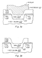
- Figures 3a-d illustrate in cross sectional elevation view steps of the first preferred embodiment method of formation of single crystal GaAs regions 104 in recesses in single crystal silicon substrate 102 as follows.
- a second preferred embodiment method follows the steps (a) through (e) of the first preferred embodiment method, but applies when GaAs 106 that lifts-off fractures along a more vertical line and leaves GaAs projection 120 as illustrated in Figure 4a.
- the location of the fracture line depends upon the thickness of GaAs layer 106, the thickness of oxide 108, and the amount of photoresist 112 overlap over oxide 108.
- the fracture line for cantilevered GaAs 106 is similar after application of an ultrasonic rinse.
- the second preferred embodiment method then proceeds as follows.
- GaAs 104 in recesses in substrate 102 by the preferred embodiment methods and standard GaAs processing are relatively low temperature processes, usually below 800 degrees C to prevent arsenic out-diffusion, so circuitry formed in the silicon surface regions of substrate 102 away from GaAs 104 could include materials such as silicides and tungsten.
- devices such as MESFETs and JFETs may be fabricated in GaAs regions 104 by standard processing, and the GaAs devices interconnected to the circuitry formed in silicon substrate 102 away from GaAs 104. Any aluminum or gold metallization would be applied after devices had been fabricated in GaAs 104.
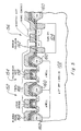
- Figure 5 illustrates MOSFETs 152 and 154 in silicon substrate 102 interconnected to MESFET 156 in single crystal GaAs 104.
- the structure of Figure 5 is simplified in order to show both standard twin-well CMOS devices with polysilicon gates 158 and field oxide 160 isolation together with an n -channel MESFET with boron lattice-damage isolation 162 in GaAs 104.
- the wafer is covered by about 3,000 ⁇ 10 ⁇ 10 m (3,000 ⁇ ) of SiO2/Si3N4/SiO2 with the nitride inserted to prevent gallium diffusion during the MBE growth of the GaAs.
- windows are opened in the oxide/nitride/oxide and recesses three ⁇ m deep are etched in the silicon substrate by RIE.
- the GaAs outside of the recesses is removed by the first preferred embodiment method.
- MESFETs are then formed by standard recessed gate processing with Ti/Pt/Au Schottky gate and Au/Ge/Ni ohmic source/drain contacts.
- Ti:W/Au metallization 166 with plasma oxide 168 insulator interconnects the CMOS (or other silicon devices) with the MESFETs (or other GaAs devices). Further interconnections, passivation, bonding, and packaging completes the chip.
- the recessed material may be other materials such as silicon-on-insulator, germanium, compound semiconductors, or other comples structure including a heavily doped silicon substrate with a lightly doped epilayer containing p and n wells for CMOS devices and bipolar regions together with trench isolation between the regions as in BiCMOS;
- the growth of the semiconductor in the recesses could be by metalorganic chemical vapor deposition (MOCVD), metalorganic MBE (MOMBE), low pressure CVD, sputtering, and so forth;
- the grown layer may be a stack of sublayers such as GaAs and Al x Ga 1- x As to permit fabrication of heterojunction bipolar transistors, the dimensions and shapes of the recesses may be varied such as some deep recesses that are filled by a second application of the preferred embodiment methods; and various crystal-de
- the invention provides the advantage of planar regions of a first semiconductor in a layer of a second semiconductor.
Landscapes
- Recrystallisation Techniques (AREA)
- Junction Field-Effect Transistors (AREA)
- Physical Deposition Of Substances That Are Components Of Semiconductor Devices (AREA)
- Drying Of Semiconductors (AREA)
- Bipolar Transistors (AREA)
Claims (15)
- Procédé de fabrication d'un dispositif à semi-conducteur, comprenant les étapes de :a) dépôt d'une couche de masque sur la surface d'une première couche d'un premier matériau semi-conducteur,b) formation d'au moins un évidement masqué dans ladite première couche du premier matériau semi-conducteur, ledit évidement étant entouré par ladite couche de masque,c) dépôt d'une seconde couche d'un second matériau semi-conducteur sur ladite première couche masquée et évidée, ladite seconde couche ayant une épaisseur à peu près égale à la profondeur dudit évidement,d) retrait de ladite seconde couche sauf au-dessus dudit évidement plus des régions adjacentes, ete) retrait dudit masque et ainsi retrait d'à peu près tout le reste de ladite seconde couche à l'extérieur dudit évidement.
- Procédé selon la revendication 1, comprenant en outre, l'étape d':
- application de vibrations au produit de l'étape e) et ainsi retrait de toutes les portions restantes de ladite seconde couche à l'extérieur dudit évidement. - Procédé selon la revendication 1, dans lequel :- ledit premier matériau semi-conducteur est du silicium, et- ledit second matériau semi-conducteur est du InxAlyGa1-x-y pour diverses valeurs non négatives de x,y dans la gamme de 0 ≦ x + y ≦ 1.0.
- Procédé selon la revendication 1, dans lequel :- ledit premier matériau semi-conducteur est du silicium,- ledit second matériau semi-conducteur est du GaAs,- ledit masque est en dioxyde de silicium, et- ledit retrait dans l'étape d) est réalisé par photolitographie.
- Procédé de fabrication d'un dispositif semi-conducteur comprenant les étapes de :a) dépôt d'une couche de masque sur la surface d'une première couche d'un premier matériau semi-conducteur,b) formation d'au moins un évidement masqué dans ladite première couche du premier matériau semi-conducteur, ledit évidement étant entouré par ladite couche de masque,c) dépôt d'une seconde couche d'un second matériau semi-conducteur sur ladite première couche évidée et masquée, ladite seconde couche ayant une épaisseur à peu près égale à la profondeur dudit évidement,d) retrait de ladite seconde couche sauf au-dessus dudit évidement plus des régions adjacentes,e) retrait dudit masque,f) formation d'une couche plane sur ladite première couche plus le reste de ladite seconde couche avec les portions dudit reste faisant saillie au-dessus du plan de ladite première couche et s'étendant également à travers ladite couche plane,g) retrait desdites portions en saillie en utilisant ladite couche plane comme masque, eth) retrait de ladite couche plane.
- Procédé selon la revendication 5, comprenant en outre l'étape d':
- application de vibrations au produit de l'étape e) avant la formation de ladite couche plane. - Procédé selon la revendication 5, dans lequel :- ledit premier matériau semi-conducteur est du silicium, et- ledit second matériau semi-conducteur est du InxAlyGa1-x-y As pour diverses valeurs non négatives de x,y dans la gamme de 0 ≦ x + y ≦ 1.0.
- Procédé selon la revendication 5, dans lequel :- ledit premier matériau semi-conducteur est du silicium,- ledit second matériau semi-conducteur est du GaAs,- ledit masque est en dioxide de silicium,- ladite couche plane est en photorésist, et- ledit retrait de l'étape d) est réalisé par photolitographie.
- Procédé selon la revendication 5, dans lequel ladite formation de l'étape f) est réalisée par rotation sur photorésist suivie d'une attaque pour exposer lesdites portions.
- Procédé selon la revendication 1, comprenant les étapes suivantes de fabrication d'un circuit intégré :- formation de dispositifs dans la première couche d'un premier matériau semi-conducteur,- formation dudit au moins un évidement masqué dans ladite première couche,- dépôt de la seconde couche du second matériau semi-conducteur sur ladite première couche évidée et masquée,- retrait de ladite seconde couche sauf au-dessus dudit évidement plus des régions adjacentes,- retrait dudit masque,- formation de dispositifs dans ladite seconde partie de couche, au-dessus dudit évidement,- formation d'électrodes et d'interconnexions desdits dispositifs dans ladite première couche et dans ladite partie de seconde couche, et- emballage de ladite première couche et de ladite partie de seconde couche plus les dispositifs et les électrodes et les interconnexions.
- Procédé selon la revendication 10, comprenant les étapes supplémentaires de :- après l'étape f), formation d'une couche plane sur ladite première couche plus le reste de ladite seconde couche avec les portions dudit reste s'étendant en saillie au-dessus du plan de ladite première couche et également à travers ladite couche plane,- retrait desdites portions en utilisant ladite couche plane comme masque, et- retrait de ladite couche plane.
- Procédé selon la revendication 11, comprenant en outre l'étape d' :
- application de vibrations au produit de l'étape f) avant la formation de ladite couche plane. - Procédé selon la revendication 10, dans lequel :- ledit premier matériau semi-conducteur est du silicium, et- ledit second matériau semi-conducteur est du InxAlyGa1-x-y As pour diverses valeurs non négatives de x,y dans la gamme de 0 ≦ x + y ≦ 1.0.
- Procédé selon la revendication 11, dans lequel :- ledit premier matériau semi-conducteur est du silicium,- ledit second matériau semi-conducteur est du GaAs,- ledit masque est en dioxyde de silicium,- ladite couche plane est en photorésist, et- ledit retrait de l'étape e) de la revendication 10, est réalisé par photolithographie.
- Procédé selon la revendication 10, dans lequel ladite formation de l'étape f) est réalisée par rotation sur photorésist suivie d'une attaque pour exposer lesdites portions.
Applications Claiming Priority (2)
| Application Number | Priority Date | Filing Date | Title |
|---|---|---|---|
| US07/224,965 US4910164A (en) | 1988-07-27 | 1988-07-27 | Method of making planarized heterostructures using selective epitaxial growth |
| US224965 | 1988-07-27 |
Publications (3)
| Publication Number | Publication Date |
|---|---|
| EP0352471A2 EP0352471A2 (fr) | 1990-01-31 |
| EP0352471A3 EP0352471A3 (fr) | 1991-03-06 |
| EP0352471B1 true EP0352471B1 (fr) | 1995-10-18 |
Family
ID=22842969
Family Applications (1)
| Application Number | Title | Priority Date | Filing Date |
|---|---|---|---|
| EP89111209A Expired - Lifetime EP0352471B1 (fr) | 1988-07-27 | 1989-06-20 | Procédé de planariser de dispositifs semiconducteurs |
Country Status (5)
| Country | Link |
|---|---|
| US (1) | US4910164A (fr) |
| EP (1) | EP0352471B1 (fr) |
| JP (1) | JP2686322B2 (fr) |
| KR (1) | KR0166958B1 (fr) |
| DE (1) | DE68924564T2 (fr) |
Families Citing this family (52)
| Publication number | Priority date | Publication date | Assignee | Title |
|---|---|---|---|---|
| US5013682A (en) * | 1986-10-22 | 1991-05-07 | Texas Instruments Incorporated | Method for selective epitaxy using a WSI mask |
| EP0365875B1 (fr) * | 1988-10-28 | 1995-08-09 | Texas Instruments Incorporated | Recuit sous encapsulant |
| GB2228617A (en) * | 1989-02-27 | 1990-08-29 | Philips Electronic Associated | A method of manufacturing a semiconductor device having a mesa structure |
| US5202284A (en) * | 1989-12-01 | 1993-04-13 | Hewlett-Packard Company | Selective and non-selective deposition of Si1-x Gex on a Si subsrate that is partially masked with SiO2 |
| US4971928A (en) * | 1990-01-16 | 1990-11-20 | General Motors Corporation | Method of making a light emitting semiconductor having a rear reflecting surface |
| US5084409A (en) * | 1990-06-26 | 1992-01-28 | Texas Instruments Incorporated | Method for patterned heteroepitaxial growth |
| US5110410A (en) * | 1990-08-13 | 1992-05-05 | Texas Instruments Incorporated | Zinc sulfide planarization |
| EP0496215B1 (fr) * | 1991-01-21 | 1995-08-30 | Siemens Aktiengesellschaft | Méthode pour la formation d'un concept structural avec matériau supraconducteur à haute température |
| FR2687008B1 (fr) * | 1992-02-05 | 2001-06-22 | Patrick Launay | Procede de fabrication de structures actives et dispositifs semiconducteurs ainsi obtenus. |
| US5279974A (en) * | 1992-07-24 | 1994-01-18 | Santa Barbara Research Center | Planar PV HgCdTe DLHJ fabricated by selective cap layer growth |
| US5443685A (en) * | 1993-11-01 | 1995-08-22 | At&T Corp. | Composition and method for off-axis growth sites on nonpolar substrates |
| JP2970425B2 (ja) * | 1994-09-26 | 1999-11-02 | 日本電気株式会社 | バイポーラトランジスタの製造方法 |
| KR0162865B1 (ko) * | 1995-03-09 | 1999-02-01 | 김은영 | 반도체 패턴 측면의 에피성장율 조절방법 |
| US5659640A (en) * | 1995-06-27 | 1997-08-19 | Lucent Technologies Inc. | Integrated waveguide having an internal optical grating |
| US6316820B1 (en) | 1997-07-25 | 2001-11-13 | Hughes Electronics Corporation | Passivation layer and process for semiconductor devices |
| US6392257B1 (en) * | 2000-02-10 | 2002-05-21 | Motorola Inc. | Semiconductor structure, semiconductor device, communicating device, integrated circuit, and process for fabricating the same |
| US6693033B2 (en) | 2000-02-10 | 2004-02-17 | Motorola, Inc. | Method of removing an amorphous oxide from a monocrystalline surface |
| AU2001257346A1 (en) | 2000-05-31 | 2001-12-11 | Motorola, Inc. | Semiconductor device and method for manufacturing the same |
| WO2002009187A2 (fr) * | 2000-07-24 | 2002-01-31 | Motorola, Inc. | Diodes a heterojonction tunnel et processus de fabrication de celles-ci |
| US6638838B1 (en) | 2000-10-02 | 2003-10-28 | Motorola, Inc. | Semiconductor structure including a partially annealed layer and method of forming the same |
| US20020096683A1 (en) * | 2001-01-19 | 2002-07-25 | Motorola, Inc. | Structure and method for fabricating GaN devices utilizing the formation of a compliant substrate |
| US6673646B2 (en) | 2001-02-28 | 2004-01-06 | Motorola, Inc. | Growth of compound semiconductor structures on patterned oxide films and process for fabricating same |
| WO2002082551A1 (fr) | 2001-04-02 | 2002-10-17 | Motorola, Inc. | Structure de semi-conducteur a courant de fuite attenue |
| US6709989B2 (en) | 2001-06-21 | 2004-03-23 | Motorola, Inc. | Method for fabricating a semiconductor structure including a metal oxide interface with silicon |
| US6992321B2 (en) | 2001-07-13 | 2006-01-31 | Motorola, Inc. | Structure and method for fabricating semiconductor structures and devices utilizing piezoelectric materials |
| US20030010992A1 (en) * | 2001-07-16 | 2003-01-16 | Motorola, Inc. | Semiconductor structure and method for implementing cross-point switch functionality |
| US6646293B2 (en) | 2001-07-18 | 2003-11-11 | Motorola, Inc. | Structure for fabricating high electron mobility transistors utilizing the formation of complaint substrates |
| US7019332B2 (en) | 2001-07-20 | 2006-03-28 | Freescale Semiconductor, Inc. | Fabrication of a wavelength locker within a semiconductor structure |
| US6693298B2 (en) | 2001-07-20 | 2004-02-17 | Motorola, Inc. | Structure and method for fabricating epitaxial semiconductor on insulator (SOI) structures and devices utilizing the formation of a compliant substrate for materials used to form same |
| US6855992B2 (en) * | 2001-07-24 | 2005-02-15 | Motorola Inc. | Structure and method for fabricating configurable transistor devices utilizing the formation of a compliant substrate for materials used to form the same |
| US6667196B2 (en) | 2001-07-25 | 2003-12-23 | Motorola, Inc. | Method for real-time monitoring and controlling perovskite oxide film growth and semiconductor structure formed using the method |
| US6589856B2 (en) | 2001-08-06 | 2003-07-08 | Motorola, Inc. | Method and apparatus for controlling anti-phase domains in semiconductor structures and devices |
| US6639249B2 (en) | 2001-08-06 | 2003-10-28 | Motorola, Inc. | Structure and method for fabrication for a solid-state lighting device |
| US20030034491A1 (en) | 2001-08-14 | 2003-02-20 | Motorola, Inc. | Structure and method for fabricating semiconductor structures and devices for detecting an object |
| US6673667B2 (en) | 2001-08-15 | 2004-01-06 | Motorola, Inc. | Method for manufacturing a substantially integral monolithic apparatus including a plurality of semiconductor materials |
| US20030036217A1 (en) * | 2001-08-16 | 2003-02-20 | Motorola, Inc. | Microcavity semiconductor laser coupled to a waveguide |
| US20030071327A1 (en) * | 2001-10-17 | 2003-04-17 | Motorola, Inc. | Method and apparatus utilizing monocrystalline insulator |
| US6916717B2 (en) * | 2002-05-03 | 2005-07-12 | Motorola, Inc. | Method for growing a monocrystalline oxide layer and for fabricating a semiconductor device on a monocrystalline substrate |
| US20040012037A1 (en) * | 2002-07-18 | 2004-01-22 | Motorola, Inc. | Hetero-integration of semiconductor materials on silicon |
| US20040069991A1 (en) * | 2002-10-10 | 2004-04-15 | Motorola, Inc. | Perovskite cuprate electronic device structure and process |
| US20040070312A1 (en) * | 2002-10-10 | 2004-04-15 | Motorola, Inc. | Integrated circuit and process for fabricating the same |
| US7169619B2 (en) | 2002-11-19 | 2007-01-30 | Freescale Semiconductor, Inc. | Method for fabricating semiconductor structures on vicinal substrates using a low temperature, low pressure, alkaline earth metal-rich process |
| US6885065B2 (en) | 2002-11-20 | 2005-04-26 | Freescale Semiconductor, Inc. | Ferromagnetic semiconductor structure and method for forming the same |
| US7020374B2 (en) * | 2003-02-03 | 2006-03-28 | Freescale Semiconductor, Inc. | Optical waveguide structure and method for fabricating the same |
| US6965128B2 (en) * | 2003-02-03 | 2005-11-15 | Freescale Semiconductor, Inc. | Structure and method for fabricating semiconductor microresonator devices |
| US20040164315A1 (en) * | 2003-02-25 | 2004-08-26 | Motorola, Inc. | Structure and device including a tunneling piezoelectric switch and method of forming same |
| US7514328B2 (en) * | 2003-06-26 | 2009-04-07 | Mears Technologies, Inc. | Method for making a semiconductor device including shallow trench isolation (STI) regions with a superlattice therebetween |
| KR20130047813A (ko) * | 2011-10-31 | 2013-05-09 | 삼성전자주식회사 | Iii-v족 화합물 반도체층을 포함하는 반도체 소자 및 그 제조방법 |
| DE102014107167B4 (de) * | 2014-05-21 | 2022-04-21 | OSRAM Opto Semiconductors Gesellschaft mit beschränkter Haftung | Verfahren zur Herstellung eines Halbleiterbauelements mit einer Strukturschicht mit einer Mehrzahl von dreidimensionalen Strukturelementen und strahlungsemittierendes Halbleiterbauelement mit einer Strukturschicht mit einer Mehrzahl von dreidimensionalen Strukturelementen |
| US9378950B1 (en) * | 2015-05-22 | 2016-06-28 | Stratio | Methods for removing nuclei formed during epitaxial growth |
| EP3758046B1 (fr) * | 2019-06-28 | 2026-04-15 | Nokia Solutions and Networks Oy | Procédé de combinaison de matériau de silicium et de matériau iii-v et dispositif associé |
| DE102020209927A1 (de) | 2020-08-06 | 2022-02-10 | Robert Bosch Gesellschaft mit beschränkter Haftung | Einebnen von Materialerhebungen auf Halbleiterschichten |
Family Cites Families (6)
| Publication number | Priority date | Publication date | Assignee | Title |
|---|---|---|---|---|
| US3401449A (en) * | 1965-10-24 | 1968-09-17 | Texas Instruments Inc | Method of fabricating a metal base transistor |
| US3322581A (en) * | 1965-10-24 | 1967-05-30 | Texas Instruments Inc | Fabrication of a metal base transistor |
| US3764409A (en) * | 1969-09-29 | 1973-10-09 | Hitachi Ltd | Method for fabricating a semiconductor component for a semiconductor circuit |
| EP0191504B1 (fr) * | 1980-04-10 | 1989-08-16 | Massachusetts Institute Of Technology | Méthode de fabrication de feuilles en matériau cristallin |
| JPS6276645A (ja) * | 1985-09-30 | 1987-04-08 | Toshiba Corp | 複合半導体結晶体構造 |
| DE3727517C2 (de) * | 1987-08-18 | 1995-06-01 | Licentia Gmbh | Verfahren zur Herstellung isolierter Halbleiterbereiche in einem Halbleiterkörper und damit hergestellte strukturierte Halbleiterkörper |
-
1988
- 1988-07-27 US US07/224,965 patent/US4910164A/en not_active Expired - Lifetime
-
1989
- 1989-06-20 DE DE68924564T patent/DE68924564T2/de not_active Expired - Fee Related
- 1989-06-20 EP EP89111209A patent/EP0352471B1/fr not_active Expired - Lifetime
- 1989-07-27 KR KR1019890010745A patent/KR0166958B1/ko not_active Expired - Fee Related
- 1989-07-27 JP JP1195377A patent/JP2686322B2/ja not_active Expired - Lifetime
Non-Patent Citations (1)
| Title |
|---|
| JOURNAL OF THE ELECTROCHEMICAL SOCIETY, vol. 130, no. 10, October 1983, pp. 2072-2075; A.Z. LI et al.: "Aspects of GaAs selective area growth by molecular beam epitaxy with patterning by Si02 masking" * |
Also Published As
| Publication number | Publication date |
|---|---|
| KR0166958B1 (ko) | 1999-02-01 |
| JPH02168631A (ja) | 1990-06-28 |
| EP0352471A3 (fr) | 1991-03-06 |
| KR900002405A (ko) | 1990-02-28 |
| EP0352471A2 (fr) | 1990-01-31 |
| DE68924564D1 (de) | 1995-11-23 |
| US4910164A (en) | 1990-03-20 |
| DE68924564T2 (de) | 1996-03-21 |
| JP2686322B2 (ja) | 1997-12-08 |
Similar Documents
| Publication | Publication Date | Title |
|---|---|---|
| US4910164A (en) | Method of making planarized heterostructures using selective epitaxial growth | |
| US20040012037A1 (en) | Hetero-integration of semiconductor materials on silicon | |
| US5312765A (en) | Method of fabricating three dimensional gallium arsenide microelectronic device | |
| US5131963A (en) | Silicon on insulator semiconductor composition containing thin synthetic diamone films | |
| US7504311B2 (en) | Structure and method of integrating compound and elemental semiconductors for high-performance CMOS | |
| US4614564A (en) | Process for selectively patterning epitaxial film growth on a semiconductor substrate | |
| EP0143656B1 (fr) | Dispositif semi-conducteur à semi-conducteurs composés et procédé de fabrication | |
| EP0372412B1 (fr) | Méthode de fabrication d'un film semiconducteur électriquement isolé du substrat | |
| US4472729A (en) | Recrystallized three dimensional integrated circuit | |
| EP0032211A2 (fr) | Procédé pour la fabrication d'une couche en silicium partiellement polycristalline et partiellement monocristalline | |
| US4619033A (en) | Fabricating of a CMOS FET with reduced latchup susceptibility | |
| US4914053A (en) | Heteroepitaxial selective-area growth through insulator windows | |
| US4593457A (en) | Method for making gallium arsenide NPN transistor with self-aligned base enhancement to emitter region and metal contact | |
| JPH05235312A (ja) | 半導体基板及びその製造方法 | |
| US5324671A (en) | Method of fabrication an integrated circuit including bipolar and field effect devices | |
| US5084409A (en) | Method for patterned heteroepitaxial growth | |
| JPH05198543A (ja) | 半導体基板の製造方法および半導体基板 | |
| EP0352472A2 (fr) | Hétéroépitaxie de matériaux semiconducteurs à résaux inégaux | |
| US5360755A (en) | Method of manufacturing a dual field effect transistor | |
| US7235809B2 (en) | Semiconductor channel on insulator structure | |
| US5234845A (en) | Method of manufacturing semiconductor IC using selective poly and EPI silicon growth | |
| CN115911032A (zh) | 具有共享的电隔离的多种器件类型的单片集成 | |
| US5885847A (en) | Method of fabricating a compound semiconductor device | |
| EP0293979A2 (fr) | Structure d'oxyde isolant sans bird-beak pour circuits intégrés | |
| EP0383034B1 (fr) | Circuit intégré et son procédé de fabrication |
Legal Events
| Date | Code | Title | Description |
|---|---|---|---|
| PUAI | Public reference made under article 153(3) epc to a published international application that has entered the european phase |
Free format text: ORIGINAL CODE: 0009012 |
|
| AK | Designated contracting states |
Kind code of ref document: A2 Designated state(s): DE FR GB IT NL |
|
| PUAL | Search report despatched |
Free format text: ORIGINAL CODE: 0009013 |
|
| AK | Designated contracting states |
Kind code of ref document: A3 Designated state(s): DE FR GB IT NL |
|
| 17P | Request for examination filed |
Effective date: 19910828 |
|
| 17Q | First examination report despatched |
Effective date: 19930423 |
|
| ITF | It: translation for a ep patent filed | ||
| GRAA | (expected) grant |
Free format text: ORIGINAL CODE: 0009210 |
|
| AK | Designated contracting states |
Kind code of ref document: B1 Designated state(s): DE FR GB IT NL |
|
| REF | Corresponds to: |
Ref document number: 68924564 Country of ref document: DE Date of ref document: 19951123 |
|
| ET | Fr: translation filed | ||
| PLBE | No opposition filed within time limit |
Free format text: ORIGINAL CODE: 0009261 |
|
| STAA | Information on the status of an ep patent application or granted ep patent |
Free format text: STATUS: NO OPPOSITION FILED WITHIN TIME LIMIT |
|
| 26N | No opposition filed | ||
| PGFP | Annual fee paid to national office [announced via postgrant information from national office to epo] |
Ref country code: NL Payment date: 20010319 Year of fee payment: 13 |
|
| PGFP | Annual fee paid to national office [announced via postgrant information from national office to epo] |
Ref country code: GB Payment date: 20010502 Year of fee payment: 13 |
|
| PGFP | Annual fee paid to national office [announced via postgrant information from national office to epo] |
Ref country code: FR Payment date: 20010531 Year of fee payment: 13 |
|
| PGFP | Annual fee paid to national office [announced via postgrant information from national office to epo] |
Ref country code: DE Payment date: 20010627 Year of fee payment: 13 |
|
| REG | Reference to a national code |
Ref country code: GB Ref legal event code: IF02 |
|
| PG25 | Lapsed in a contracting state [announced via postgrant information from national office to epo] |
Ref country code: GB Free format text: LAPSE BECAUSE OF NON-PAYMENT OF DUE FEES Effective date: 20020620 |
|
| PG25 | Lapsed in a contracting state [announced via postgrant information from national office to epo] |
Ref country code: NL Free format text: LAPSE BECAUSE OF NON-PAYMENT OF DUE FEES Effective date: 20030101 Ref country code: DE Free format text: LAPSE BECAUSE OF NON-PAYMENT OF DUE FEES Effective date: 20030101 |
|
| GBPC | Gb: european patent ceased through non-payment of renewal fee |
Effective date: 20020620 |
|
| PG25 | Lapsed in a contracting state [announced via postgrant information from national office to epo] |
Ref country code: FR Free format text: LAPSE BECAUSE OF NON-PAYMENT OF DUE FEES Effective date: 20030228 |
|
| NLV4 | Nl: lapsed or anulled due to non-payment of the annual fee |
Effective date: 20030101 |
|
| REG | Reference to a national code |
Ref country code: FR Ref legal event code: ST |
|
| PG25 | Lapsed in a contracting state [announced via postgrant information from national office to epo] |
Ref country code: IT Free format text: LAPSE BECAUSE OF NON-PAYMENT OF DUE FEES;WARNING: LAPSES OF ITALIAN PATENTS WITH EFFECTIVE DATE BEFORE 2007 MAY HAVE OCCURRED AT ANY TIME BEFORE 2007. THE CORRECT EFFECTIVE DATE MAY BE DIFFERENT FROM THE ONE RECORDED. Effective date: 20050620 |