EP0365875B1 - Recuit sous encapsulant - Google Patents
Recuit sous encapsulant Download PDFInfo
- Publication number
- EP0365875B1 EP0365875B1 EP89118311A EP89118311A EP0365875B1 EP 0365875 B1 EP0365875 B1 EP 0365875B1 EP 89118311 A EP89118311 A EP 89118311A EP 89118311 A EP89118311 A EP 89118311A EP 0365875 B1 EP0365875 B1 EP 0365875B1
- Authority
- EP
- European Patent Office
- Prior art keywords
- gaas
- layer
- growth
- silicon
- temperature
- Prior art date
- Legal status (The legal status is an assumption and is not a legal conclusion. Google has not performed a legal analysis and makes no representation as to the accuracy of the status listed.)
- Expired - Lifetime
Links
Images


Classifications
-
- H—ELECTRICITY
- H10—SEMICONDUCTOR DEVICES; ELECTRIC SOLID-STATE DEVICES NOT OTHERWISE PROVIDED FOR
- H10P—GENERIC PROCESSES OR APPARATUS FOR THE MANUFACTURE OR TREATMENT OF DEVICES COVERED BY CLASS H10
- H10P95/00—Generic processes or apparatus for manufacture or treatments not covered by the other groups of this subclass
- H10P95/90—Thermal treatments, e.g. annealing or sintering
- H10P95/904—Thermal treatments, e.g. annealing or sintering of Group III-V semiconductors
-
- H—ELECTRICITY
- H10—SEMICONDUCTOR DEVICES; ELECTRIC SOLID-STATE DEVICES NOT OTHERWISE PROVIDED FOR
- H10P—GENERIC PROCESSES OR APPARATUS FOR THE MANUFACTURE OR TREATMENT OF DEVICES COVERED BY CLASS H10
- H10P14/00—Formation of materials, e.g. in the shape of layers or pillars
- H10P14/20—Formation of materials, e.g. in the shape of layers or pillars of semiconductor materials
- H10P14/22—Formation of materials, e.g. in the shape of layers or pillars of semiconductor materials using physical deposition, e.g. vacuum deposition or sputtering
-
- H—ELECTRICITY
- H10—SEMICONDUCTOR DEVICES; ELECTRIC SOLID-STATE DEVICES NOT OTHERWISE PROVIDED FOR
- H10P—GENERIC PROCESSES OR APPARATUS FOR THE MANUFACTURE OR TREATMENT OF DEVICES COVERED BY CLASS H10
- H10P14/00—Formation of materials, e.g. in the shape of layers or pillars
- H10P14/20—Formation of materials, e.g. in the shape of layers or pillars of semiconductor materials
- H10P14/29—Formation of materials, e.g. in the shape of layers or pillars of semiconductor materials characterised by the substrates
- H10P14/2901—Materials
- H10P14/2902—Materials being Group IVA materials
- H10P14/2905—Silicon, silicon germanium or germanium
-
- H—ELECTRICITY
- H10—SEMICONDUCTOR DEVICES; ELECTRIC SOLID-STATE DEVICES NOT OTHERWISE PROVIDED FOR
- H10P—GENERIC PROCESSES OR APPARATUS FOR THE MANUFACTURE OR TREATMENT OF DEVICES COVERED BY CLASS H10
- H10P14/00—Formation of materials, e.g. in the shape of layers or pillars
- H10P14/20—Formation of materials, e.g. in the shape of layers or pillars of semiconductor materials
- H10P14/32—Formation of materials, e.g. in the shape of layers or pillars of semiconductor materials characterised by intermediate layers between substrates and deposited layers
- H10P14/3202—Materials thereof
- H10P14/3214—Materials thereof being Group IIIA-VA semiconductors
- H10P14/3221—Arsenides
-
- H—ELECTRICITY
- H10—SEMICONDUCTOR DEVICES; ELECTRIC SOLID-STATE DEVICES NOT OTHERWISE PROVIDED FOR
- H10P—GENERIC PROCESSES OR APPARATUS FOR THE MANUFACTURE OR TREATMENT OF DEVICES COVERED BY CLASS H10
- H10P14/00—Formation of materials, e.g. in the shape of layers or pillars
- H10P14/20—Formation of materials, e.g. in the shape of layers or pillars of semiconductor materials
- H10P14/32—Formation of materials, e.g. in the shape of layers or pillars of semiconductor materials characterised by intermediate layers between substrates and deposited layers
- H10P14/3242—Structure
- H10P14/3244—Layer structure
- H10P14/3251—Layer structure consisting of three or more layers
-
- H—ELECTRICITY
- H10—SEMICONDUCTOR DEVICES; ELECTRIC SOLID-STATE DEVICES NOT OTHERWISE PROVIDED FOR
- H10P—GENERIC PROCESSES OR APPARATUS FOR THE MANUFACTURE OR TREATMENT OF DEVICES COVERED BY CLASS H10
- H10P14/00—Formation of materials, e.g. in the shape of layers or pillars
- H10P14/20—Formation of materials, e.g. in the shape of layers or pillars of semiconductor materials
- H10P14/34—Deposited materials, e.g. layers
- H10P14/3402—Deposited materials, e.g. layers characterised by the chemical composition
- H10P14/3414—Deposited materials, e.g. layers characterised by the chemical composition being group IIIA-VIA materials
- H10P14/3421—Arsenides
-
- H—ELECTRICITY
- H10—SEMICONDUCTOR DEVICES; ELECTRIC SOLID-STATE DEVICES NOT OTHERWISE PROVIDED FOR
- H10P—GENERIC PROCESSES OR APPARATUS FOR THE MANUFACTURE OR TREATMENT OF DEVICES COVERED BY CLASS H10
- H10P14/00—Formation of materials, e.g. in the shape of layers or pillars
- H10P14/20—Formation of materials, e.g. in the shape of layers or pillars of semiconductor materials
- H10P14/38—Formation of materials, e.g. in the shape of layers or pillars of semiconductor materials characterised by treatments done after the formation of the materials
-
- Y—GENERAL TAGGING OF NEW TECHNOLOGICAL DEVELOPMENTS; GENERAL TAGGING OF CROSS-SECTIONAL TECHNOLOGIES SPANNING OVER SEVERAL SECTIONS OF THE IPC; TECHNICAL SUBJECTS COVERED BY FORMER USPC CROSS-REFERENCE ART COLLECTIONS [XRACs] AND DIGESTS
- Y10—TECHNICAL SUBJECTS COVERED BY FORMER USPC
- Y10S—TECHNICAL SUBJECTS COVERED BY FORMER USPC CROSS-REFERENCE ART COLLECTIONS [XRACs] AND DIGESTS
- Y10S148/00—Metal treatment
- Y10S148/003—Anneal
-
- Y—GENERAL TAGGING OF NEW TECHNOLOGICAL DEVELOPMENTS; GENERAL TAGGING OF CROSS-SECTIONAL TECHNOLOGIES SPANNING OVER SEVERAL SECTIONS OF THE IPC; TECHNICAL SUBJECTS COVERED BY FORMER USPC CROSS-REFERENCE ART COLLECTIONS [XRACs] AND DIGESTS
- Y10—TECHNICAL SUBJECTS COVERED BY FORMER USPC
- Y10S—TECHNICAL SUBJECTS COVERED BY FORMER USPC CROSS-REFERENCE ART COLLECTIONS [XRACs] AND DIGESTS
- Y10S148/00—Metal treatment
- Y10S148/065—Gp III-V generic compounds-processing
-
- Y—GENERAL TAGGING OF NEW TECHNOLOGICAL DEVELOPMENTS; GENERAL TAGGING OF CROSS-SECTIONAL TECHNOLOGIES SPANNING OVER SEVERAL SECTIONS OF THE IPC; TECHNICAL SUBJECTS COVERED BY FORMER USPC CROSS-REFERENCE ART COLLECTIONS [XRACs] AND DIGESTS
- Y10—TECHNICAL SUBJECTS COVERED BY FORMER USPC
- Y10S—TECHNICAL SUBJECTS COVERED BY FORMER USPC CROSS-REFERENCE ART COLLECTIONS [XRACs] AND DIGESTS
- Y10S438/00—Semiconductor device manufacturing: process
- Y10S438/902—Capping layer
-
- Y—GENERAL TAGGING OF NEW TECHNOLOGICAL DEVELOPMENTS; GENERAL TAGGING OF CROSS-SECTIONAL TECHNOLOGIES SPANNING OVER SEVERAL SECTIONS OF THE IPC; TECHNICAL SUBJECTS COVERED BY FORMER USPC CROSS-REFERENCE ART COLLECTIONS [XRACs] AND DIGESTS
- Y10—TECHNICAL SUBJECTS COVERED BY FORMER USPC
- Y10S—TECHNICAL SUBJECTS COVERED BY FORMER USPC CROSS-REFERENCE ART COLLECTIONS [XRACs] AND DIGESTS
- Y10S438/00—Semiconductor device manufacturing: process
- Y10S438/933—Germanium or silicon or Ge-Si on III-V
Definitions
- the present invention relates to growth of semiconductor materials and devices, and, more particularly, to heteroepitaxial growth such as gallium arsenide on silicon and devices in such heterostructures.
- GaAs gallium arsenide
- Selective recrystallization of amorphous GaAs can use the high resistivity of noncrystalline GaAs; see, for example, A.Christou et al, Formation of (100) GaAs on (100) Silicon by Laser Recrystallization, 48 Appl. Phys. Lett. 1516 (1986).
- Post-growth annealing by itself has been shown to be effective at reducing the global defect in GaAs layers on silicon substrates; however, there is insufficient data at this time to determine its effectivenes at lowering the density of device degrading threading dislocations.
- Fan et al., U.S.Pat.No. 4,632,712 interrupts the GaAs growth to trap threading dislocations.
- a number of workers have studied the use of either compositional or thermally cycled superlattices during the growth process for dislocation control; see J.W. Lee, Proc. 1986 Int'I. Symp. on GaAs and Related Compounds 111 (1987), T. Soga et al, 26 Japan. J. Appl. Phys.
- the present invention provides a lattice matched annealing cap for semiconductor layers, both for heteroepitaxial growth and for implant activation, and devices fabricated with the annealed semiconductor.
- Preferred embodiments include heteroepitaxially grown GaAs on silicon with an AlxGa1-xAs capping layer plus further GaAs grown on the capping layer after the anneal; devices are fabricated in this further GaAs layer.
- Other preferred embodiments include Al x Ga 1-x As capping of GaAs followed by implantation of dopants through the Al x Ga 1-x As plus an activation anneal for fabrication of devices such as MESFETs and heterojunction bipolar transistors.
- the first preferred embodiment heteroepitaxial structure shown in schematic cross sectional elevation view in Figure 1 and generally denoted 100, includes silicon substrate 102,1.5 ⁇ m thick GaAs buffer layer 104, 0.1 ⁇ m thick AlxGa 1-x As layer 106, AlAs layer 108 which is only a few atomic layers thick, and GaAs layer 110 of thickness 2.5 ⁇ m (microns).
- Active devices such as MESFET 112 and JFETs may be fabricated in GaAs layer 110, or layer 110 could be grown to include both GaAs and AlxGa 1-x As layers and heterojunction bipolar transistors fabricated in layer 110.
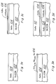
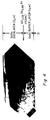
- the first preferred embodiment method of fabrication of the first preferred embodiment structure includes the time-temperature growth illustrated in Figure 2 and the steps illustrated in cross sectional elevation view in Figures 3a-d as follows:
- GaAs and silicon have quite different coefficients of thermal expansion, so a low growth temperature will yield less thermal stress in the resultant structure.
- MBE growth will be preferable to the higher MOCVD growth of GaAs on silicon.
- MBE growth is cleaner than MOCVD growth due to the large amounts of carbon present from the metalorganic compounds used in MOCVD.
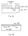
- the second preferred embodiment method uses a Al x Ga 1-x As capping layer for the activation anneal of implanted GaAs includes the following steps as illustrated in cross sectional elevation view in Figures 5a-b.
- Third preferred embodiment method uses an epitaxial Al o . 5 Ga o . 5 As cap as both an anneal cap and an implant spacer.
- Figures 6a-b illustrate the base formation process of an emitter-down overgrowth heterojunction bipolar transistor showing both the starting first epi in Figure 6a and the base implant profile in Figure 6b.
- a spacer layer such as epitaxial Al o . 5 Ga o . 5 As 308 or silicon nitride can be deposited over the base area to act as a spacer for adjusting the base implant depth.
- the peak in the base doping concentration should occur at the emitter-base junction.
- the spacer thickness can be adjusted such that the peak of the implant occurs at the emitter/base interface for a given implant energy and fluence.
- the high (50%) aluminum concentration in the Al x Ga 1-x As spacer layer 308 permits easy removal from the underlying GaAs base surface after the activation anneal of the base implant.
- Afurther advantage of using Al x Ga 1-x As 308 as the spacer layer instead of silicon nitride or other such material is that upon annealing AlxGa 1-x As acts as an arsenic rich cap to keep the base surface region from decomposing.
- Rapid thermal annealing precludes the use of arsenic over-pressure due to process complexity in a single wafer process; however, the arsenic rich cap, Al x Ga 1-x As 308, helps maintain the GaAs surface perfection.
- the GaAs collector layer can be grown onto the base layer.
- Fourth preferred embodiment method is similar to the third preferred embodiment except that the base is implanted through an AlxGa1-xAs spacer layer into the collector layer to fabricate an emitter-up HBT. Again, after the anneal, which is typically rapid thermal annealing, the Al x Ga 1-x As cap is removed and the emitter is grown.
- a spacer layer of Al x Ga 1-x As with x - 0.5 on top of the structure is used for improved implant activation and better ohmic contacts.
- the base is contacted by a P+ implant, through the spacer, and the collector is reached by a N+ implant, through the spacer.
- These implants require an activation anneal, typically rapid thermal annealing, where the use of arsenic over-pressure is not practical.
- the Al x Ga 1-x As spacer layer will keep the surface arsenic rich and after its removal in HF, ohmic contact formation on the good, arsenic rich GaAs will be better.
- an Al x Ga 1-x As/GaAs superlattice may be used as the anneal cap of AIGaAs in MBE; in this situation, the Al x Ga 1-x As may be grown at a higher temperature (e.g., 600°C) and the GaAs at a lower temperature (e.g., 550°C) to obtain the benefits of both a compositional plus thermal-cycled superlattice (which blocks dislocation propagation) and an Al x Ga 1-x As anneal cap.
- the buffer layer and the top layer could be different materials such as Al x Ga 1-x As with different x and each of the layers could include sublayers with different x; indeed, material systems other than AIGaAs, such as GaAsP, InGaAs, InAIGaAsP, etc. or even II-VI systems, could be used with the lower vapor pressure component used as the capping layer. Additionally, various growth temperatures and temperature cycling could be used in the various material systems. Lattice matching of the cap to the annealed layer need only be close enough to avoid defects; thus a thin strained layer cap could also be used.
- the annealing process could be a furnace anneal, a rapid thermal anneal, or other type of anneal or combination of anneals, and could be used with other material systems.
- the starting substrate for the preferred embodiments and variations could be complex such as silicon- on-insulator or include recesses and amorphous material patterns such as silicon dioxide patterns on silicon.
- devices other than HBTs could be fabricated (such as MESFETs and JFETs) by implantation and capped anneal, and integrated circuits of the various devices could be fabricated.
- the related-material capped anneal the corresponding interfaces such as emitter/base and ohmic/semiconductor will have improved surface state densities and lower specific resistivities.
Landscapes
- Bipolar Transistors (AREA)
- Recrystallisation Techniques (AREA)
- Physical Deposition Of Substances That Are Components Of Semiconductor Devices (AREA)
- Junction Field-Effect Transistors (AREA)
Claims (7)
Applications Claiming Priority (2)
| Application Number | Priority Date | Filing Date | Title |
|---|---|---|---|
| US26423788A | 1988-10-28 | 1988-10-28 | |
| US264237 | 1988-10-28 |
Publications (3)
| Publication Number | Publication Date |
|---|---|
| EP0365875A2 EP0365875A2 (fr) | 1990-05-02 |
| EP0365875A3 EP0365875A3 (en) | 1990-07-11 |
| EP0365875B1 true EP0365875B1 (fr) | 1995-08-09 |
Family
ID=23005164
Family Applications (1)
| Application Number | Title | Priority Date | Filing Date |
|---|---|---|---|
| EP89118311A Expired - Lifetime EP0365875B1 (fr) | 1988-10-28 | 1989-10-03 | Recuit sous encapsulant |
Country Status (5)
| Country | Link |
|---|---|
| US (3) | US5391515A (fr) |
| EP (1) | EP0365875B1 (fr) |
| JP (1) | JP2791138B2 (fr) |
| KR (1) | KR0142191B1 (fr) |
| DE (1) | DE68923756T2 (fr) |
Cited By (1)
| Publication number | Priority date | Publication date | Assignee | Title |
|---|---|---|---|---|
| US9553153B1 (en) | 2015-12-02 | 2017-01-24 | International Business Machines Corporation | Post growth defect reduction for heteroepitaxial materials |
Families Citing this family (65)
| Publication number | Priority date | Publication date | Assignee | Title |
|---|---|---|---|---|
| JP2754599B2 (ja) * | 1988-10-05 | 1998-05-20 | 株式会社デンソー | 半導体装置 |
| JP2557546B2 (ja) * | 1990-03-30 | 1996-11-27 | 三菱電機株式会社 | 半導体装置の製造方法 |
| JP3587537B2 (ja) | 1992-12-09 | 2004-11-10 | 株式会社半導体エネルギー研究所 | 半導体装置 |
| US5834362A (en) * | 1994-12-14 | 1998-11-10 | Fujitsu Limited | Method of making a device having a heteroepitaxial substrate |
| US6188090B1 (en) | 1995-08-31 | 2001-02-13 | Fujitsu Limited | Semiconductor device having a heteroepitaxial substrate |
| US6274464B2 (en) | 1998-02-06 | 2001-08-14 | Texas Instruments Incorporated | Epitaxial cleaning process using HCL and N-type dopant gas to reduce defect density and auto doping effects |
| US6080644A (en) * | 1998-02-06 | 2000-06-27 | Burr-Brown Corporation | Complementary bipolar/CMOS epitaxial structure and process |
| JP2000068284A (ja) | 1998-08-19 | 2000-03-03 | Sharp Corp | ヘテロ接合バイポーラトランジスタの製造方法及びパワーアンプ |
| US6566256B1 (en) * | 1999-04-16 | 2003-05-20 | Gbl Technologies, Inc. | Dual process semiconductor heterostructures and methods |
| US6693033B2 (en) | 2000-02-10 | 2004-02-17 | Motorola, Inc. | Method of removing an amorphous oxide from a monocrystalline surface |
| US6392257B1 (en) * | 2000-02-10 | 2002-05-21 | Motorola Inc. | Semiconductor structure, semiconductor device, communicating device, integrated circuit, and process for fabricating the same |
| US6429103B1 (en) * | 2000-04-13 | 2002-08-06 | Motorola, Inc. | MOCVD-grown emode HIGFET buffer |
| US6653706B1 (en) * | 2000-05-08 | 2003-11-25 | The Board Of Trustees Of The Leland Stanford Junior University | Low temperature grown optical detector |
| AU2001257346A1 (en) * | 2000-05-31 | 2001-12-11 | Motorola, Inc. | Semiconductor device and method for manufacturing the same |
| US6477285B1 (en) | 2000-06-30 | 2002-11-05 | Motorola, Inc. | Integrated circuits with optical signal propagation |
| AU2001274913A1 (en) * | 2000-06-30 | 2002-01-14 | Motorola, Inc. | Thin compound semiconductor structure |
| US6501973B1 (en) | 2000-06-30 | 2002-12-31 | Motorola, Inc. | Apparatus and method for measuring selected physical condition of an animate subject |
| US6410941B1 (en) | 2000-06-30 | 2002-06-25 | Motorola, Inc. | Reconfigurable systems using hybrid integrated circuits with optical ports |
| JP4120184B2 (ja) * | 2000-06-30 | 2008-07-16 | セイコーエプソン株式会社 | 実装用微小構造体および光伝送装置 |
| AU2001264987A1 (en) * | 2000-06-30 | 2002-01-14 | Motorola, Inc., A Corporation Of The State Of Delware | Hybrid semiconductor structure and device |
| US6427066B1 (en) | 2000-06-30 | 2002-07-30 | Motorola, Inc. | Apparatus and method for effecting communications among a plurality of remote stations |
| WO2002009187A2 (fr) * | 2000-07-24 | 2002-01-31 | Motorola, Inc. | Diodes a heterojonction tunnel et processus de fabrication de celles-ci |
| US6555946B1 (en) | 2000-07-24 | 2003-04-29 | Motorola, Inc. | Acoustic wave device and process for forming the same |
| US6597112B1 (en) * | 2000-08-10 | 2003-07-22 | Itt Manufacturing Enterprises, Inc. | Photocathode for night vision image intensifier and method of manufacture |
| US6638838B1 (en) | 2000-10-02 | 2003-10-28 | Motorola, Inc. | Semiconductor structure including a partially annealed layer and method of forming the same |
| US6563118B2 (en) | 2000-12-08 | 2003-05-13 | Motorola, Inc. | Pyroelectric device on a monocrystalline semiconductor substrate and process for fabricating same |
| US20020096683A1 (en) * | 2001-01-19 | 2002-07-25 | Motorola, Inc. | Structure and method for fabricating GaN devices utilizing the formation of a compliant substrate |
| US6673646B2 (en) | 2001-02-28 | 2004-01-06 | Motorola, Inc. | Growth of compound semiconductor structures on patterned oxide films and process for fabricating same |
| WO2002082551A1 (fr) | 2001-04-02 | 2002-10-17 | Motorola, Inc. | Structure de semi-conducteur a courant de fuite attenue |
| US6709989B2 (en) | 2001-06-21 | 2004-03-23 | Motorola, Inc. | Method for fabricating a semiconductor structure including a metal oxide interface with silicon |
| US6992321B2 (en) | 2001-07-13 | 2006-01-31 | Motorola, Inc. | Structure and method for fabricating semiconductor structures and devices utilizing piezoelectric materials |
| US20030010992A1 (en) * | 2001-07-16 | 2003-01-16 | Motorola, Inc. | Semiconductor structure and method for implementing cross-point switch functionality |
| US6646293B2 (en) | 2001-07-18 | 2003-11-11 | Motorola, Inc. | Structure for fabricating high electron mobility transistors utilizing the formation of complaint substrates |
| US7019332B2 (en) | 2001-07-20 | 2006-03-28 | Freescale Semiconductor, Inc. | Fabrication of a wavelength locker within a semiconductor structure |
| US6693298B2 (en) | 2001-07-20 | 2004-02-17 | Motorola, Inc. | Structure and method for fabricating epitaxial semiconductor on insulator (SOI) structures and devices utilizing the formation of a compliant substrate for materials used to form same |
| US6472694B1 (en) | 2001-07-23 | 2002-10-29 | Motorola, Inc. | Microprocessor structure having a compound semiconductor layer |
| US6855992B2 (en) * | 2001-07-24 | 2005-02-15 | Motorola Inc. | Structure and method for fabricating configurable transistor devices utilizing the formation of a compliant substrate for materials used to form the same |
| US6594414B2 (en) | 2001-07-25 | 2003-07-15 | Motorola, Inc. | Structure and method of fabrication for an optical switch |
| US6585424B2 (en) | 2001-07-25 | 2003-07-01 | Motorola, Inc. | Structure and method for fabricating an electro-rheological lens |
| US6667196B2 (en) | 2001-07-25 | 2003-12-23 | Motorola, Inc. | Method for real-time monitoring and controlling perovskite oxide film growth and semiconductor structure formed using the method |
| US6639249B2 (en) | 2001-08-06 | 2003-10-28 | Motorola, Inc. | Structure and method for fabrication for a solid-state lighting device |
| US6462360B1 (en) | 2001-08-06 | 2002-10-08 | Motorola, Inc. | Integrated gallium arsenide communications systems |
| US6589856B2 (en) | 2001-08-06 | 2003-07-08 | Motorola, Inc. | Method and apparatus for controlling anti-phase domains in semiconductor structures and devices |
| US20030034491A1 (en) | 2001-08-14 | 2003-02-20 | Motorola, Inc. | Structure and method for fabricating semiconductor structures and devices for detecting an object |
| US6673667B2 (en) | 2001-08-15 | 2004-01-06 | Motorola, Inc. | Method for manufacturing a substantially integral monolithic apparatus including a plurality of semiconductor materials |
| US20030036217A1 (en) * | 2001-08-16 | 2003-02-20 | Motorola, Inc. | Microcavity semiconductor laser coupled to a waveguide |
| US20030071327A1 (en) * | 2001-10-17 | 2003-04-17 | Motorola, Inc. | Method and apparatus utilizing monocrystalline insulator |
| US6916717B2 (en) | 2002-05-03 | 2005-07-12 | Motorola, Inc. | Method for growing a monocrystalline oxide layer and for fabricating a semiconductor device on a monocrystalline substrate |
| US20040012037A1 (en) * | 2002-07-18 | 2004-01-22 | Motorola, Inc. | Hetero-integration of semiconductor materials on silicon |
| US20040070312A1 (en) * | 2002-10-10 | 2004-04-15 | Motorola, Inc. | Integrated circuit and process for fabricating the same |
| US20040069991A1 (en) * | 2002-10-10 | 2004-04-15 | Motorola, Inc. | Perovskite cuprate electronic device structure and process |
| US7169619B2 (en) | 2002-11-19 | 2007-01-30 | Freescale Semiconductor, Inc. | Method for fabricating semiconductor structures on vicinal substrates using a low temperature, low pressure, alkaline earth metal-rich process |
| US6885065B2 (en) | 2002-11-20 | 2005-04-26 | Freescale Semiconductor, Inc. | Ferromagnetic semiconductor structure and method for forming the same |
| US6965128B2 (en) * | 2003-02-03 | 2005-11-15 | Freescale Semiconductor, Inc. | Structure and method for fabricating semiconductor microresonator devices |
| US7020374B2 (en) * | 2003-02-03 | 2006-03-28 | Freescale Semiconductor, Inc. | Optical waveguide structure and method for fabricating the same |
| US20040164315A1 (en) * | 2003-02-25 | 2004-08-26 | Motorola, Inc. | Structure and device including a tunneling piezoelectric switch and method of forming same |
| WO2005036627A1 (fr) * | 2003-10-03 | 2005-04-21 | Applied Materials, Inc. | Couche absorbante pour traitement de recuit de surface dynamique |
| US7109087B2 (en) | 2003-10-03 | 2006-09-19 | Applied Materials, Inc. | Absorber layer for DSA processing |
| JP4785392B2 (ja) * | 2004-03-26 | 2011-10-05 | キヤノン株式会社 | テラヘルツ電磁波の発生素子の製造方法 |
| US20060011129A1 (en) * | 2004-07-14 | 2006-01-19 | Atomic Energy Council - Institute Of Nuclear Energy Research | Method for fabricating a compound semiconductor epitaxial wafer |
| US20070173925A1 (en) * | 2006-01-25 | 2007-07-26 | Cornova, Inc. | Flexible expandable stent |
| US20080177371A1 (en) * | 2006-08-28 | 2008-07-24 | Cornova, Inc. | Implantable devices and methods of forming the same |
| WO2009067364A1 (fr) | 2007-11-20 | 2009-05-28 | S.O.I.Tec Silicon On Insulator Technologies | Transfert de tranches à haute température |
| DE112011106054B4 (de) * | 2011-12-28 | 2023-05-25 | Intel Corporation | Methoden der Bildung von Hetero-Schichten mit reduzierter Oberflachenrauhigkeit und Defektdichte auf ortsfremden Oberflächen und die dadurch entstehenden Strukturen |
| US9721792B2 (en) | 2013-09-16 | 2017-08-01 | Applied Materials, Inc. | Method of forming strain-relaxed buffer layers |
Family Cites Families (14)
| Publication number | Priority date | Publication date | Assignee | Title |
|---|---|---|---|---|
| US4267014A (en) * | 1980-02-29 | 1981-05-12 | The United States Of America As Represented By The Secretary Of The Navy | Semiconductor encapsulant for annealing ion-implanted GaAs |
| JPS5999717A (ja) * | 1982-11-29 | 1984-06-08 | Fujitsu Ltd | 半導体装置の製造方法 |
| US4494997A (en) * | 1983-06-15 | 1985-01-22 | Westinghouse Electric Corp. | Ion implant mask and cap for gallium arsenide structures |
| JPS6012724A (ja) * | 1983-07-01 | 1985-01-23 | Agency Of Ind Science & Technol | 化合物半導体の成長方法 |
| US5091333A (en) * | 1983-09-12 | 1992-02-25 | Massachusetts Institute Of Technology | Reducing dislocations in semiconductors utilizing repeated thermal cycling during multistage epitaxial growth |
| US4699688A (en) * | 1986-07-14 | 1987-10-13 | Gte Laboratories Incorporated | Method of epitaxially growing gallium arsenide on silicon |
| US5183776A (en) * | 1986-09-26 | 1993-02-02 | Texas Instruments Incorporated | Heteroepitaxy by growth of thermally strained homojunction superlattice buffer layers |
| US4914053A (en) * | 1987-09-08 | 1990-04-03 | Texas Instruments Incorporated | Heteroepitaxial selective-area growth through insulator windows |
| US4900372A (en) * | 1987-11-13 | 1990-02-13 | Kopin Corporation | III-V on Si heterostructure using a thermal strain layer |
| JP2691721B2 (ja) * | 1988-03-04 | 1997-12-17 | 富士通株式会社 | 半導体薄膜の製造方法 |
| US5238869A (en) * | 1988-07-25 | 1993-08-24 | Texas Instruments Incorporated | Method of forming an epitaxial layer on a heterointerface |
| US4910164A (en) * | 1988-07-27 | 1990-03-20 | Texas Instruments Incorporated | Method of making planarized heterostructures using selective epitaxial growth |
| US5185288A (en) * | 1988-08-26 | 1993-02-09 | Hewlett-Packard Company | Epitaxial growth method |
| US5246878A (en) * | 1992-03-27 | 1993-09-21 | Bell Communications Research, Inc. | Capping layer preventing deleterious effects of As--P exchange |
-
1989
- 1989-10-03 EP EP89118311A patent/EP0365875B1/fr not_active Expired - Lifetime
- 1989-10-03 DE DE68923756T patent/DE68923756T2/de not_active Expired - Fee Related
- 1989-10-27 JP JP1281611A patent/JP2791138B2/ja not_active Expired - Fee Related
- 1989-10-27 KR KR1019890015510A patent/KR0142191B1/ko not_active Expired - Fee Related
-
1992
- 1992-06-17 US US07/900,226 patent/US5391515A/en not_active Expired - Lifetime
-
1995
- 1995-06-07 US US08/475,724 patent/US5659188A/en not_active Expired - Lifetime
-
1996
- 1996-06-05 US US08/658,294 patent/US5744375A/en not_active Expired - Fee Related
Non-Patent Citations (1)
| Title |
|---|
| APPLIED PHYSICS LETTERS, vol. 50, no. 7, February 16, 1987, pp. 407-409, American Institute of Physics, New York, US ; R.D. DUPUIS et al. : "Low-threshold high-efficiency A1GaAs-GaAs double-heterostructure injection lasers grown on Si substrates by metalorganic chemical vapor deposition" * |
Cited By (1)
| Publication number | Priority date | Publication date | Assignee | Title |
|---|---|---|---|---|
| US9553153B1 (en) | 2015-12-02 | 2017-01-24 | International Business Machines Corporation | Post growth defect reduction for heteroepitaxial materials |
Also Published As
| Publication number | Publication date |
|---|---|
| JPH02244729A (ja) | 1990-09-28 |
| US5659188A (en) | 1997-08-19 |
| DE68923756T2 (de) | 1996-03-07 |
| DE68923756D1 (de) | 1995-09-14 |
| KR0142191B1 (ko) | 1998-07-15 |
| US5744375A (en) | 1998-04-28 |
| JP2791138B2 (ja) | 1998-08-27 |
| EP0365875A2 (fr) | 1990-05-02 |
| EP0365875A3 (en) | 1990-07-11 |
| US5391515A (en) | 1995-02-21 |
| KR900007061A (ko) | 1990-05-09 |
Similar Documents
| Publication | Publication Date | Title |
|---|---|---|
| US5391515A (en) | Capped anneal | |
| US5238869A (en) | Method of forming an epitaxial layer on a heterointerface | |
| EP0447327B1 (fr) | Dispositif semi-conducteur à hétérostructure | |
| US4876219A (en) | Method of forming a heteroepitaxial semiconductor thin film using amorphous buffer layers | |
| US5256550A (en) | Fabricating a semiconductor device with strained Si1-x Gex layer | |
| JP3093904B2 (ja) | 化合物半導体結晶の成長方法 | |
| EP0514018A2 (fr) | Procédé de fabrication d'une hétéro-structure semi-conductrice à faible taux de défauts et composants obtenus par ledit procédé | |
| EP0352472A2 (fr) | Hétéroépitaxie de matériaux semiconducteurs à résaux inégaux | |
| US4914053A (en) | Heteroepitaxial selective-area growth through insulator windows | |
| EP0430562B1 (fr) | Hétérostructure semi-conductrice et méthode pour sa fabrication | |
| JP3024584B2 (ja) | 半導体装置の製造方法 | |
| US5084409A (en) | Method for patterned heteroepitaxial growth | |
| JPH03188619A (ja) | 異種基板上への3―5族化合物半導体のヘテロエピタキシャル成長法 | |
| US5183776A (en) | Heteroepitaxy by growth of thermally strained homojunction superlattice buffer layers | |
| JP3438116B2 (ja) | 化合物半導体装置及びその製造方法 | |
| EP0413546B1 (fr) | Méthode pour former une couche de semiconducteur composé | |
| JP3227083B2 (ja) | バイポーラトランジスタの作製方法 | |
| US4948752A (en) | Method of making sagfets on buffer layers | |
| US5183778A (en) | Method of producing a semiconductor device | |
| US5341006A (en) | Semiconductor device having diffusion-preventing layer between III-V layer and IV layer | |
| JP3592922B2 (ja) | 化合物半導体基板 | |
| JP2555885B2 (ja) | ゲルマニウム・砒化ガリウム接合の製造方法 | |
| JP2920923B2 (ja) | 半導体装置の製造方法 | |
| JP2705374B2 (ja) | Iii−v化合物半導体上のiv族元素半導体形成方法 | |
| JPH11204437A (ja) | 半導体装置およびその製造方法 |
Legal Events
| Date | Code | Title | Description |
|---|---|---|---|
| PUAI | Public reference made under article 153(3) epc to a published international application that has entered the european phase |
Free format text: ORIGINAL CODE: 0009012 |
|
| AK | Designated contracting states |
Kind code of ref document: A2 Designated state(s): DE FR GB IT NL |
|
| PUAL | Search report despatched |
Free format text: ORIGINAL CODE: 0009013 |
|
| AK | Designated contracting states |
Kind code of ref document: A3 Designated state(s): DE FR GB IT NL |
|
| 17P | Request for examination filed |
Effective date: 19901220 |
|
| 17Q | First examination report despatched |
Effective date: 19930407 |
|
| GRAA | (expected) grant |
Free format text: ORIGINAL CODE: 0009210 |
|
| AK | Designated contracting states |
Kind code of ref document: B1 Designated state(s): DE FR GB IT NL |
|
| PG25 | Lapsed in a contracting state [announced via postgrant information from national office to epo] |
Ref country code: NL Free format text: LAPSE BECAUSE OF FAILURE TO SUBMIT A TRANSLATION OF THE DESCRIPTION OR TO PAY THE FEE WITHIN THE PRESCRIBED TIME-LIMIT Effective date: 19950809 |
|
| ITF | It: translation for a ep patent filed | ||
| REF | Corresponds to: |
Ref document number: 68923756 Country of ref document: DE Date of ref document: 19950914 |
|
| ET | Fr: translation filed | ||
| NLV1 | Nl: lapsed or annulled due to failure to fulfill the requirements of art. 29p and 29m of the patents act | ||
| PLBE | No opposition filed within time limit |
Free format text: ORIGINAL CODE: 0009261 |
|
| STAA | Information on the status of an ep patent application or granted ep patent |
Free format text: STATUS: NO OPPOSITION FILED WITHIN TIME LIMIT |
|
| 26N | No opposition filed | ||
| REG | Reference to a national code |
Ref country code: GB Ref legal event code: IF02 |
|
| PGFP | Annual fee paid to national office [announced via postgrant information from national office to epo] |
Ref country code: FR Payment date: 20041004 Year of fee payment: 16 |
|
| PGFP | Annual fee paid to national office [announced via postgrant information from national office to epo] |
Ref country code: DE Payment date: 20041029 Year of fee payment: 16 |
|
| PG25 | Lapsed in a contracting state [announced via postgrant information from national office to epo] |
Ref country code: IT Free format text: LAPSE BECAUSE OF NON-PAYMENT OF DUE FEES Effective date: 20051003 |
|
| PG25 | Lapsed in a contracting state [announced via postgrant information from national office to epo] |
Ref country code: DE Free format text: LAPSE BECAUSE OF NON-PAYMENT OF DUE FEES Effective date: 20060503 |
|
| PG25 | Lapsed in a contracting state [announced via postgrant information from national office to epo] |
Ref country code: FR Free format text: LAPSE BECAUSE OF NON-PAYMENT OF DUE FEES Effective date: 20060630 |
|
| REG | Reference to a national code |
Ref country code: FR Ref legal event code: ST Effective date: 20060630 |
|
| PGFP | Annual fee paid to national office [announced via postgrant information from national office to epo] |
Ref country code: GB Payment date: 20070918 Year of fee payment: 19 |
|
| GBPC | Gb: european patent ceased through non-payment of renewal fee |
Effective date: 20081003 |
|
| PG25 | Lapsed in a contracting state [announced via postgrant information from national office to epo] |
Ref country code: GB Free format text: LAPSE BECAUSE OF NON-PAYMENT OF DUE FEES Effective date: 20081003 |