EP0353163A2 - Integrierte Schaltung mit Bipolar-CMOS-Schaltung - Google Patents
Integrierte Schaltung mit Bipolar-CMOS-Schaltung Download PDFInfo
- Publication number
- EP0353163A2 EP0353163A2 EP89402168A EP89402168A EP0353163A2 EP 0353163 A2 EP0353163 A2 EP 0353163A2 EP 89402168 A EP89402168 A EP 89402168A EP 89402168 A EP89402168 A EP 89402168A EP 0353163 A2 EP0353163 A2 EP 0353163A2
- Authority
- EP
- European Patent Office
- Prior art keywords
- bipolar transistor
- gate
- transistor
- base
- bipolar
- Prior art date
- Legal status (The legal status is an assumption and is not a legal conclusion. Google has not performed a legal analysis and makes no representation as to the accuracy of the status listed.)
- Granted
Links
Images




Classifications
-
- G—PHYSICS
- G11—INFORMATION STORAGE
- G11C—STATIC STORES
- G11C7/00—Arrangements for writing information into, or reading information out from, a digital store
-
- H—ELECTRICITY
- H03—ELECTRONIC CIRCUITRY
- H03K—PULSE TECHNIQUE
- H03K3/00—Circuits for generating electric pulses; Monostable, bistable or multistable circuits
- H03K3/01—Details
- H03K3/012—Modifications of generator to improve response time or to decrease power consumption
-
- H—ELECTRICITY
- H03—ELECTRONIC CIRCUITRY
- H03K—PULSE TECHNIQUE
- H03K3/00—Circuits for generating electric pulses; Monostable, bistable or multistable circuits
- H03K3/02—Generators characterised by the type of circuit or by the means used for producing pulses
- H03K3/021—Generators characterised by the type of circuit or by the means used for producing pulses by the use, as active elements, of more than one type of element or means, e.g. BIMOS, composite devices such as IGBT
-
- H—ELECTRICITY
- H03—ELECTRONIC CIRCUITRY
- H03K—PULSE TECHNIQUE
- H03K3/00—Circuits for generating electric pulses; Monostable, bistable or multistable circuits
- H03K3/02—Generators characterised by the type of circuit or by the means used for producing pulses
- H03K3/353—Generators characterised by the type of circuit or by the means used for producing pulses by the use, as active elements, of field-effect transistors with internal or external positive feedback
- H03K3/356—Bistable circuits
- H03K3/356104—Bistable circuits using complementary field-effect transistors
Definitions
- the present invention generally relates to an integrated circuit having a bipolar-CMOS circuit, and particularly to a flip-flop circuit having a bipolar-CMOS circuit.
- a flip-flop is widely used in various electronic circuits such as a register and a latch circuit.
- a flip-flop is formed by NAND gates or NOR gates.
- NAND gates or NOR gates are commonly used in various electronic circuits.
- NOR gates are commonly used in various electronic circuits.
- a flip-flop made up of NAND gates operates faster than a flip-flop made up of NOR gates.
- NAND gates G1 and G2 are supplied with complementary inputs A and B, respectively.
- Complementary outputs Q and XQ of the NAND gates G1 and G2 are supplied, as inputs, with the NAND gates G2 and G1, respectively.
- a NAND gate outputs a low logic level (hereinafter simply referred to as L) when both the inputs are a high logic level (hereinafter simply referred to as H).
- L low logic level
- H high logic level
- the two inputs of the NAND gate G1 are switched to L and H and the output Q thereof is changed from L to H.
- both the inputs of the NAND gate G2 change to H, and the output XQ thereof is switched from H to L.
- the flip-flop is settled.
- the output of one of the NAND gates does not change from H to L until the output of the other NAND gate has changed to H.
- the output of the NAND gate G2 changes from H to L when the output of the NAND gate G1 has changed to H. That is, there is a delay of time between the outputs Q and XQ. This delay is equal to one stage of NAND gate. The delay occurring between the outputs Q and XQ causes a skew.
- the NAND gate G1 includes P-channel metal oxide semiconductor transistors P21 and P22 connected to a high-potential power source V DD , and N-channel metal oxide semiconductor transistors N21 and N22.
- a P-channel metal oxide semiconductor is simply referred to as PMOS transistor
- an N-channel metal oxide semiconductor is simply referred to as NMOS transistor.
- the PMOS transistors P21 and P22, and the NMOS transistors N21 and N22 define a NAND logic.
- An NPN bipolar transistor Q21 is used for charging the output Q quickly, and an NPN bipolar transistor Q23 is used for discharging the output Q quickly. That is, the bipolar transistors Q21 and Q23 function to drive a load coupled to the output of the NAND gate G1.
- the NAND gate G1 is a bipolar-CMOS (Bi-CMOS) circuit.
- NMOS transistors N23 and N24 are used for drawing a charge at the base of the bipolar transistor Q21.
- An NMOS transistor N25 connected to a low potential power source functions to draw a charge at the base of the bipolar transistor Q23.
- the NAND gate G2 is formed in the same manner as the NAND gate G1, and consists of PMOS transistors P23, P24, NMOS transistors N26 - N30, and bipolar transistors Q22 and Q24.
- the PMOS transistor P24 is switched from ON to OFF, and the bipolar transistor Q22 turns OFF. Further, the NMOS transistors N26 and N28 turn ON.
- the aforementioned change in the output Q from L to H is transferred to the gates of the NMOS transistors N27 and N29, so that the NMOS transistors N27 and N28 turn ON.
- a charge at the output XQ passes through the NMOS transistors N26 and N27. Then a part of the charge is applied to the base of the bipolar transistor Q24, and the remaining charge passes through the NMOS transistor N30.
- the bipolar transistor Q24 is turned ON by the application of part of the charge from the output XQ.
- a more specific object of the present invention is to provide a flip-flop having Bi-CMOS circuits having a reduced delay appearing between the outputs of the flip-flop.
- an integrated circuit including first gate means for inputting first and second inputs and generating a first output indicative of a first logic operation result of the first gate means.
- the first gate means has a first output terminal passing the first output.
- the first gate means includes first CMOS means for receiving the first and second inputs and generating the first logic operation result, and first bipolar transistor means for generating the first output from the first logic operation result.
- the first bipolar transistor means includes a first bipolar transistor charging the first output terminal, and a second bipolar transistor discharging the first output terminal.
- the integrated circuit includes second gate means for inputting third and fourth inputs and generating a second output indicative of a second logic operation result of the second gate means.
- the second gate means has a second output terminal passing the second output.
- the second gate means includes second CMOS means for receiving the third and fourth inputs and generating the second logic operation result, and second bipolar transistor means for generating the second output from the second logic operation result, the second bipolar transistor means including a third bipolar transistor charging the second output terminal, and a fourth bipolar transistor discharging the second output terminal.
- the first and third inputs are complementary inputs.
- the first output serves as the fourth input, and the second output serves as the second input.
- the first and second outputs are complementary outputs.
- the integrated circuit includes discharge means for discharging a base of the first bipolar transistor of the first bipolar transistor means in response to a change in the third input and for discharging a base of the third bipolar transistor of the second bipolar transistor means in response to a change in the first input.
- the integrated circuit includes charge means for charging a base of the second bipolar transistor of the first bipolar transistor means in response to the change in the third input and for charging a base of the fourth bipolar transistor of the second bipolar transistor means in response to the change in the first input.
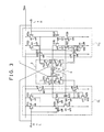
- FIG.3 A description is given of a first preferred embodiment of the present invention with reference to FIG.3.
- FIG.3 those parts which are the same as those shown in FIG.2 are given the same references.
- An essential feature of the first embodiment is that a base discharge circuit 3 and a base charge circuit 4 are provided for the NAND gates G1 and G2.
- Each of the base discharge circuit 3 and the base charge circuit 4 is supplied with the complementary inputs A and B.
- the NAND gates G1 and G2, the base discharge circuit 3, and the base charge circuit 4 form a flip-flop.
- the base discharge circuit 3 is made up of PMOS transistors P3 and P4.
- the gates of the PMOS transistors P3 and P4 are supplied with the inputs B and A, respectively.
- the source of the PMOS transistor P3 is connected to the base of the bipolar transistor Q21 in the NAND gate G1, and the drain thereof is connected to a low-potential power source (ground).
- the source of the PMOS transistor P4 is connected to the base of the bipolar transistor Q22, and the drain thereof is connected to the low-potential power source.
- the PMOS transistor P3 functions to discharge the base of the bipolar transistor Q21 in response to a change in the input B.
- the PMOS transistor P4 functions to discharge the base of the bipolar transistor Q22 in response to a change in the input A.
- the base charge circuit 4 is made up of PMOS transistors P5 and P6.
- the gates of the PMOS transistors P5 and P6 are supplied with the inputs B and A, respectively.
- the source of the PMOS transistor P5 is connected to the collector of the bipolar transistor Q23 and the output Q of the NAND gate G1.
- the drain of the PMOS transistor P5 is connected to the base of the bipolar transistor Q23.
- the source of the PMOS transistor P6 is connected to the collector of the transistor Q24 and the output XQ of the NAND gate G2.
- the drain of the PMOS transistor P6 is connected to the base of the bipolar transistor Q24.
- the PMOS transistor P5 functions to charge the base of the bipolar transistor Q23 in response to a change in the input A.
- the PMOS transistor P6 functions to charge the base of the bipolar transistor Q24 in response to a change in the input A.
- the flip-flop shown in FIG.3 operates as follows.
- the PMOS transistor P21 turns ON.
- the PMOS transistors P4 and P6 change from OFF to ON.
- the PMOS transistor P24 turns OFF, and simultaneously the PMOS transistors P3 and P5 turn OFF.
- the PMOS transistor P4 Since the PMOS transistor P4 turns ON when the input A changes from H to L, the base of the bipolar transistor Q22 is discharged through the PMOS transistor P4 so that the bipolar transistor Q22 starts turning OFF. At the same time as the PMOS transistor P4 turns ON, the PMOS transistor P6 turns ON. Thus, a charge at the output XQ of the NAND gate G2 is allowed to pass through the PMOS transistor P6. This charge passes through the base of the bipolar transistor Q24 and the NMOS transistor N30, so that the bipolar transistor Q24 starts turning ON. Thus, the charge at the output XQ is allowed to pass through the bipolar transistor Q24, and the level of the output XQ starts decreasing.
- the level of the output XQ of the NAND gate G2 starts decreasing when the input A of the NAND gate G1 changes from H to L, or in other words, the level of the output XQ starts decreasing before the level of the output Q of the NAND gate G1 changes.
- the flip-flop of the first embodiment can operate at a speed higher than that of the flip-flop shown in FIG.2. It is noted that the output XQ of the NAND gate G2 starts decreasing after the output Q of the NAND gate G1 changes from L to H in FIG.2.
- the output Q When the output XQ is being discharged, the output Q starts changing from L to H in response to a change of the bipolar transistor Q21 from OFF to ON. This change of the output Q is transferred to the NMOS transistors N27 and N29. At this time, the NMOS transistors N26 and N27 have already been turned ON in response to a change in the input B from L to H. Thus, discharging of the output XQ is facilitated through the NMOS transistors N26, N27 and N30.
- the bipolar transistor Q21 When the bipolar transistor Q21 turns ON, the NMOS transistor N25 turns ON. Thus, the base of the bipolar transistor Q23 is discharged through the NMOS transistor N25, so that it turns OFF. Therefore, the output Q of the NAND gate G1 is charged up to the potential V DD through the bipolar transistor Q21.
- the output XQ of the NAND gate G2 starts changing when the input A of the NAND gate G1 changes. It is particularly noted that in the above-mentioned operation, the output XQ starts changing in response to a change in the input A. Hence, a reduced time difference between the outputs Q and XQ can be obtained.
- An essential feature of the second embodiment is that a flip-flop is constructed by a small number of elements, compared with the first embodiment.
- the flip-flop according to the second embodiment can operate faster than the flip-flop according to the first embodiment.
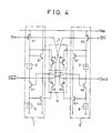
- FIG.4 is a circuit diagram of the second embodiment. As is illustrated, the second embodiment is formed by substituting the NAND gates G1 and G2 for Bi-CMOS type inverters 1 and 2, respectively.
- the base discharge circuit 3 and the base charge circuit 4 are the same as those shown in FIG.3.
- the inverter 1 includes an input circuit and an output circuit.
- the input circuit of the inverter 1 handles a logic operation of the inverter 1, and the output circuit thereof serves as a driver circuit.
- the input circuit is made up of a PMOS transistor P1, an NMOS transistor N1, and loads (impedance circuits) 5 and 6, all of which are connected in series as shown in FIG.4. That is, the source of the PMOS transistor P1 is connected to the high-potential power source V DD , and the drain thereof is connected to one of the two ends of the load 5.
- the gate of the PMOS transistor P1 is supplied with an input Din (corresponding to the input A shown in FIG.3).
- the other end of the load 5 is connected to the drain of the NMOS transistor N1, through which an output Dout (corresponding to the output XQ) is drawn.
- the source of the NMOS transistor N1 is connected to one of the two ends of the load 6, and the other end thereof is connected to the low-potential power source (not shown).
- the output circuit of the inverter 1 is made up of two NPN bipolar transistors Q1 and Q3, which are connected in series.
- the collector of the bipolar transistor Q1 is connected to the high-potential power source V DD , and the emitter thereof is connected to the collector of the bipolar transistor Q3.
- the base of the bipolar transistor Q1 is connected to the drain of the PMOS transistor P1.
- the base of the bipolar transistor Q3 is connected to the source of the NMOS transistor N1, and the emitter thereof is connected to the low-potential power source.
- the inverter 2 is formed in the same manner as the inverter 1.
- An input Din is supplied to the inverter 2, which provides an output Dout.
- the inputs Din and Din are complementary inputs, and the outputs Dout and Dout are complementary outputs.
- the inverter 2 is made up of a PMOS transistor P2, an NMOS transistor N2, two bipolar transistors Q2 and Q4, and two loads 7 and 8.
- FIG.5A is a circuit diagram of a CMOS inverter.
- the CMOS inverter consists of PMOS and NMOS transistors P1 and N1 connected in series.
- An input IN is supplied to the gates of the PMOS and NMOS transistors P1 and N1, and an output OUT is drawn from the mutually connected drains of the PMOS and NMOS transistors P1 and N1.
- FIG.5B a modified inverter formed by combining the CMOS inverter shown in FIG.5A and bipolar transistors Q1 and Q3.
- Resistors R1 and R3 function to discharge the bases of the bipolar transistors Q1 and Q3, respectively.
- the input IN is H
- the PMOS and NMOS transistors P1 and N1 are OFF and ON, respectively
- the bipolar transistors Q1 and Q3 are OFF and ON, respectively.
- the output OUT is L.
- the input IN is L
- the PMOS and NMOS transistors P1 and N1 are ON and OFF, respectively
- the bipolar transistors Q1 and Q3 are ON and OFF, respectively.
- the output OUT is H.
- Each of the inverters 1 and 2 is formed in a similar manner to the modified inverter shown in FIG.5B.
- a flip-flop By cross-connecting the inverters of FIG.5B, a flip-flop can be formed.
- the flip-flop thus configured is constructed by a smaller number of structural elements than a number of structural elements for a NAND gate type flip-flop or a NOR gate type flip-flop. Additionally, a capacitance coupled to the input of the Bi-CMOS inverter type flip-flop is smaller than those for the other type flip-flops. It is however noted that a conventional Bi-CMOS inverter type flip-flop presents a delay which occurs between the complementary outputs.
- the base discharge circuit 3 and the base charge circuit 4 are provided according to the second embodiment.
- the base discharge circuit 3 starts discharging the base of the bipolar transistor Q1 or Q2 in response to a change in the input Din or Din .
- the base charge circuit 4 starts charging the base of the bipolar transistor Q3 or Q4 in response to a change in the input Din or Din .
- the loads 5 to 8 may be formed by resistors or MOS transistors.
- FIG.6 is a circuit diagram of a flip-flop formed by using NMOS transistors N3 to N6 to form the loads 5 to 8.
- the drains of the NMOS transistors N3 and N4 are connected to the drains of the PMOS transistors P1 and P2, respectively.
- the gates of the NMOS transistors N3 and N4 are connected to the outputs Dout and Dout , respectively, and the sources thereof are connected to the low-potential power source.
- the drains of the NMOS transistors N5 and N6 are connected to the sources of the NMOS transistors N1 and N2, respectively.
- the source of the NMOS transistors N5 and N6 are connected to the low-potential power source.
- the gates of the NMOS transistors N5 and N6 are connected to the outputs Dout and Dout, respectively.
- the flip-flop shown in FIG.6 is stable in the state where the inputs Din and Din are H and L, respectively, and the outputs Dout and Dout are H and L, respectively.
- the PMOS transistors P1, P4 and P6 are OFF, and the PMOS transistors P2, P3 and p5 are ON.
- the NMOS transistors N1, N3 and N6 are ON and the NMOS transistors N2, N4 an N5 are OFF.
- the bipolar transistors Q1 and Q4 are OFF, and the bipolar transistors Q2 and Q3 are ON.
- the PMOS transistors P1, P4 and P6 are turned ON, and the PMOS transistors P2, P3 and P5 are turned OFF.
- the output Dout is still H and the output Dout is still L.
- the NMOS transistors N1, N3 and N6 are ON, and the NMOS transistors N2, N4 and N5 are OFF.
- the base potential of the bipolar transistor Q1 increases up to an intermediate potential based on ON resistances of the PMOS transistor P1 and the NMOS transistor N1.
- the bipolar transistor Q1 turns toward ON and passes a current based on the intermediate potential of the base thereof.
- the output Dout increases up to an intermediate potential H′ (L ⁇ H′ ⁇ H) based on ON resistances of the bipolar transistors Q1 and Q3.
- the NMOS transistors N2, N4 and N5 are switched to an ON state based on the intermediate potential H′.
- a charge at the base of the bipolar transistor Q3 starts passing through the NMOS transistor N5, so that the bipolar transistor Q3 starts turning OFF.
- the PMOS transistor P4 since the PMOS transistor P4 turns ON when the input Din changes from H to L, a charge at the base of the bipolar transistor Q2 is allowed to pass through the PMOS transistor P4. That is, the potential of the base of the bipolar transistor Q2 starts decreasing at the same time as the input Din changes from H to L.
- the bipolar transistor Q2 turns toward OFF.
- the base of the bipolar transistor Q2 is discharged through the NMOS transistor N4 which is in the ON state based on the intermediate potential H′. Thereby, discharging of the base of the bipolar transistor Q2 is accelerated.
- the PMOS transistor P6 turns ON at the same time as the input Din changes from H to L. Thereby, a charge at the output Dout is caused to pass through the PMOS transistor P6. At this time, the NMOS transistor N6 is ON. Therefore, the charge at the output Dout passes through the PMOS transistor P6 and then the NMOS transistor N6. Thus, the potential of the output Dout starts decreasing to become an intermediate potential L′ (H ⁇ L′ ⁇ L). Simultaneously, the bipolar transistor Q4 starts turning ON, and a part of the charge at the output Dout is allowed to pass through the bipolar transistor Q4.
- the increasing intermediate potential H, of the output Dout is also applied to the gate of the NMOS transistor N2, which starts turning ON.
- a base current from the output Dout which is still H starts charging the base of the bipolar transistor Q4, so that the bipolar transistor Q4 is facilitated to turn ON.
- the decreasing intermediate potential L′ of the output Dout is applied to the gate of the NMOS transistor N3.
- the bipolar transistor Q1 is facilitated to turn ON. That is, ON resistance of the bipolar transistor Q1 is further decreased, so that the output Dout further increases. Thereby, ON resistance of the NMOS transistor N2 is further reduced, so that the output Dout further decreases.
- the base discharge circuit 3 and the base charge circuit 4 cause changes in the outputs Dout and Dout at the same time as the levels of the inputs Din and Din change. Then, changes of the inverter 1 and 2 facilitate changes of the inverter 2 and 1, respectively. As a result, the outputs Dout and Dout are quickly stabilized and there is less time difference therebetween.
- FIG.7 is a circuit diagram of a configuration for the second embodiment where the loads 5 to 8 are formed by resistors R1 through R4, respectively.
- the resistor R1 is connected between the base of the bipolar transistor Q1 and the output Dout
- the resistor R2 is connected between the base of the bipolar transistor Q2 and the output Dout.
- the resistor R3 is connected between the source of the NMOS transistor N1 and the low-potential power source.
- the resistor R4 is connected between the source of the NMOS transistor N2 and the low-potential power source.
- the flip-flop shown in FIG.7 is stable in the state where the inputs Din and Din are H and L, respectively and the outputs Dout and Dout are H and L, respectively.
- the PMOS transistors P1, P4 and P6 are OFF, and the PMOS transistors P2, P3 and P5 are ON.
- the NMOS transistors N1 and N2 are ON and OFF, respectively.
- the bipolar transistors Q1 and Q4 are OFF, and the bipolar transistors Q2 and Q3 are ON.
- the flip-flop When the inputs Din and Din change to L and H, respectively, for example, the flip-flop operates as follows. At the same time as the inputs Din and Din change, the PMOS transistors P1, P4 and P6 turn ON, and the PMOS transistors P2, P3 and P5 turn OFF. At this moment, the output Dout is still H and the output Dout is still L. Therefore, the NMOS transistors N1 and N2 are ON and OFF, respectively.
- the base potential of the bipolar transistor Q1 increases up to an intermediate potential based on ON resistances of the PMOS transistor P1 and the resistance R1.
- the bipolar transistor Q1 starts turning ON and passes a current based on the intermediate potential of the base thereof.
- the output Dout increases up to an intermediate potential H, (L ⁇ H′ ⁇ H) based on ON resistances of the bipolar transistors Q1 and Q3.
- the NMOS transistor N2 starts turning ON.
- the PMOS transistor P4 since the PMOS transistor P4 turns ON when the input Din changes from H to L, a charge at the base of the bipolar transistor Q2 is allowed to pass through the PMOS transistor P4. That is, the potential of the base of the bipolar transistor Q2 starts decreasing at the same time as the input Din changes from H to L. Then the bipolar transistor Q2 turns toward OFF.
- the base of the bipolar transistor Q2 is discharged through the NMOS transistor N2 which is in an ON state based on the increasing intermediate potential H′ at the output Dout . Thereby, discharging of the base of the bipolar transistor Q2 is facilitated through the resistor R2, the NMOS transistor N2, and the resistor R4.
- the PMOS transistor P6 turns ON at the same time as the input Din changes from H to L. Thereby, a charge at the output Dout is allowed to pass through the PMOS transistor P6 and the resistor R4. Thus, the potential of the output Dout starts decreasing to become an intermediate potential L′ (H ⁇ L′ ⁇ L). Simultaneously, the bipolar transistor Q4 starts turning ON, and a part of the charge at the output Dout is allowed to pass through the bipolar transistor Q4.
- the decreasing intermediate potential L′ of the output Dout is applied to the gate of the NMOS transistor N1, so that it starts turning OFF.
- the NMOS transistor N1 stops supplying the bipolar transistor Q3 with a base current from the high-potential power source V DD through the PMOS transistor P1 and the resistor R1.
- a charge at the base of the bipolar transistor Q3 is drawn through the resistor R3.
- the bipolar transistor Q3 turns OFF, so that the potential of the output Dout further increases.
- the increased potential of the output Dout causes a further increase of the base potential of the bipolar transistor Q1.
- ON resistance of the bipolar transistor Q1 further decreases, and the potential of the output Dout further increases.
- the potential of the output Dout further decreases.
- This causes a further decrease of the base potential of the bipolar transistor Q2.
- ON resistance of the bipolar transistor Q2 is further increased, so that a decrease of the output Dout is facilitated.
- the outputs Dout and Dout are inverted to L and H, respectively.
- the outputs Dout and Dout start changing at the same time as the inputs Din and Din change, and less time difference between the outputs Dout and Dout occurs.
- the NMOS transistors N3 and N4 shown in FIG.6 are connected to ground, and on the other hand, the resistors R1 and R2 are connected to the outputs Dout and Dout , respectively. This is based on the difference between characteristics of transistors and resistors. In case where the resistors R1 and R2 are connected to ground, current flows to ground through the resistor R1 when the input Din changes from H to L. This is wasteful of power. This holds true for the resistor R2. On the other hand, when the input Din changes from H to L, the NMOS transistor N1 in the configuration shown in FIG.7 turns OFF. Therefore, the current through the resistor R1 is inhibited from flowing to ground. This holds true for the inverter 2.
- a flip-flop according to the third embodiment includes a base discharge circuit 21 and a base charge circuit 22, which cooperate with NOR gates 11 and 12.
- the NOR gate 11 is made up of PMOS transistors P41, P42, NMOS transistors N41 through N45, and NPN bipolar transistors Q1 and Q3.
- the NOR gate 12 is made up of PMOS transistors P43, P44, NMOS transistors N46 through N50, and NPN bipolar transistors Q2 and Q4.
- the base discharge circuit 21 is made up of two NMOS transistors N51 and N52.
- the gates of the NMOS transistors N51 and N52 are supplied with the inputs Din and Din, respectively, and the drains thereof are connected to the bases of the bipolar transistors Q1 and Q2, respectively.
- the sources of the NMOS transistors N51 and N52 are connected to the low-potential power source (ground).
- the base charge circuit 22 is made up of two NMOS transistors N53 and N54.
- the gates of the NMOS transistors N53 and N54 are supplied with the inputs Din and Din, respectively, and the sources thereof are connected to the bases of the bipolar transistors Q3 and Q4, respectively.
- the drains of the NMOS transistors N53 and N54 are connected to the collectors of the bipolar transistors Q3 and Q4, respectively.
- the drains of the NMOS transistors N53 and N54 are connected to the outputs of the NOR gates 12 and 11, respectively.
- a NOR gate generates a high-level output Dout when both the inputs are L. Therefore, when the inputs Din and Din applied to the NOR gates 11 and 12 are L, the outputs Dout and Dout of the flip-flop are H and L, or L and H, respectively.
- the NMOS transistors N51 and N52 of the base discharge circuit 21 are made active when the inputs Din and Din change from L to H, respectively.
- the NMOS transistors N53 and N54 of the base charge circuit 22 are made active when the inputs Din and Din change from L to H.
- an edge trigger type register which is made up of NAND gates G5 to G8, and a flip-flop FF formed according to the present invention.
- the input Din is applied to the NAND gate G8, and a clock pulse CLK is supplied to the NAND gates G6 and G7.
- An example of the clock pulse CLK and the input Din is shown in FIG.10.
- the clock pulse CLK is L
- outputs D2 and D3 of the gates G6 and G7 are H.
- the input Din is H/L (high or low)
- the output of the NAND gate G8 is L/H
- the output of the NAND gate G5 is H/L.
- the flip-flop FF operates as indicated by the following table. TABLE D2 D3 Q XQ H H no change H L L H L H H L As shown in FIG.10(c), the output Q is delayed by a time t d from the clock pulse CLK shown in FIG.10(a).
- FIG.11 is a circuit diagram of another application of the present invention.
- the illustrated circuit is a master-slave type register.
- Two flip-flops FF1 and FF2 are formed according to the present invention.
- the master-slave type register includes four NAND gates G10 to G13 and two inverters INV1 and INV2.
- the clock pulse CLK is supplied to the NAND gates G10 and G11, and is supplied to the NAND gates G12 and G13 through the inverter INV2.
- the input Din is supplied to the NAND gate G10, and is supplied to the NAND gate G11 through the inverter INV1.
- the outputs of the NAND gates G10 and G11 are connected to inputs B′ and A′ of the flip-flop FF1, respectively.
- Outputs Q′ and XQ′ of the flip-flop are connected to the NAND gates G12 and G13, respectively.
- the outputs of the NAND gates G12 and G13 are connected to inputs B and A of the flip-flop FF2, which has outputs Q and XQ.
- FIG.12 is a timing chart of signals at different points of the master-slave type register shown in FIG.11.
Landscapes
- Logic Circuits (AREA)
- Metal-Oxide And Bipolar Metal-Oxide Semiconductor Integrated Circuits (AREA)
Applications Claiming Priority (2)
| Application Number | Priority Date | Filing Date | Title |
|---|---|---|---|
| JP189981/88 | 1988-07-29 | ||
| JP63189981A JPH0239719A (ja) | 1988-07-29 | 1988-07-29 | 半導体回路 |
Publications (3)
| Publication Number | Publication Date |
|---|---|
| EP0353163A2 true EP0353163A2 (de) | 1990-01-31 |
| EP0353163A3 EP0353163A3 (de) | 1991-05-08 |
| EP0353163B1 EP0353163B1 (de) | 1995-02-15 |
Family
ID=16250405
Family Applications (1)
| Application Number | Title | Priority Date | Filing Date |
|---|---|---|---|
| EP89402168A Expired - Lifetime EP0353163B1 (de) | 1988-07-29 | 1989-07-28 | Integrierte Schaltung mit Bipolar-CMOS-Schaltung |
Country Status (5)
| Country | Link |
|---|---|
| US (1) | US4972096A (de) |
| EP (1) | EP0353163B1 (de) |
| JP (1) | JPH0239719A (de) |
| KR (1) | KR920010998B1 (de) |
| DE (1) | DE68921112T2 (de) |
Cited By (1)
| Publication number | Priority date | Publication date | Assignee | Title |
|---|---|---|---|---|
| EP0410885A3 (en) * | 1989-07-25 | 1991-10-02 | Fujitsu Limited | Level-conversion semiconductor device |
Families Citing this family (2)
| Publication number | Priority date | Publication date | Assignee | Title |
|---|---|---|---|---|
| JP2540934B2 (ja) * | 1989-03-09 | 1996-10-09 | 三菱電機株式会社 | 論理回路装置 |
| EP0608666B1 (de) * | 1993-01-29 | 1998-04-29 | STMicroelectronics S.r.l. | Monolithisch integrierbares Zeitverzögerungsfilter |
Family Cites Families (8)
| Publication number | Priority date | Publication date | Assignee | Title |
|---|---|---|---|---|
| JPH0783252B2 (ja) * | 1982-07-12 | 1995-09-06 | 株式会社日立製作所 | 半導体集積回路装置 |
| US4645954A (en) * | 1985-10-21 | 1987-02-24 | International Business Machines Corp. | ECL to FET interface circuit for field effect transistor arrays |
| JPS62254460A (ja) * | 1986-04-26 | 1987-11-06 | Toshiba Corp | Bi−CMOS論理回路 |
| JPH0611111B2 (ja) * | 1987-03-27 | 1994-02-09 | 株式会社東芝 | BiMOS論理回路 |
| DE3878345T2 (de) * | 1987-08-17 | 1993-05-27 | Nippon Electric Co | Bimosschaltung, faehig zum betrieb bei hoher geschwindigkeit mit niedrigem verbrauch. |
| JP2593894B2 (ja) * | 1987-11-16 | 1997-03-26 | 富士通株式会社 | 半導体記憶装置 |
| JPH07109980B2 (ja) * | 1988-05-19 | 1995-11-22 | 富士通株式会社 | 半導体集積回路 |
| US4845385A (en) * | 1988-06-21 | 1989-07-04 | Silicon Connections Corporation | BiCMOS logic circuits with reduced crowbar current |
-
1988
- 1988-07-29 JP JP63189981A patent/JPH0239719A/ja active Pending
-
1989
- 1989-07-25 US US07/384,431 patent/US4972096A/en not_active Expired - Fee Related
- 1989-07-27 KR KR1019890010659A patent/KR920010998B1/ko not_active Expired
- 1989-07-28 DE DE68921112T patent/DE68921112T2/de not_active Expired - Fee Related
- 1989-07-28 EP EP89402168A patent/EP0353163B1/de not_active Expired - Lifetime
Cited By (1)
| Publication number | Priority date | Publication date | Assignee | Title |
|---|---|---|---|---|
| EP0410885A3 (en) * | 1989-07-25 | 1991-10-02 | Fujitsu Limited | Level-conversion semiconductor device |
Also Published As
| Publication number | Publication date |
|---|---|
| KR910003654A (ko) | 1991-02-28 |
| DE68921112D1 (de) | 1995-03-23 |
| EP0353163A3 (de) | 1991-05-08 |
| US4972096A (en) | 1990-11-20 |
| KR920010998B1 (ko) | 1992-12-26 |
| JPH0239719A (ja) | 1990-02-08 |
| EP0353163B1 (de) | 1995-02-15 |
| DE68921112T2 (de) | 1995-06-08 |
Similar Documents
| Publication | Publication Date | Title |
|---|---|---|
| EP0175501B1 (de) | Verzögerungsschaltung für LSI-Toranordnung | |
| US6633188B1 (en) | Sense amplifier-based flip-flop with asynchronous set and reset | |
| US4697105A (en) | CMOS programmable logic array | |
| US6563357B1 (en) | Level converting latch | |
| EP0346876B1 (de) | Integrierte Halbleiterschaltung mit einem CMOS-Inverter | |
| US20020024368A1 (en) | Flip-flop circuits having digital-to-time conversion latches therein | |
| EP0360525A2 (de) | Ausgangspufferschaltung mit einer Regelumsetzungsfunktion | |
| US20020050868A1 (en) | Function generator with adjustable oscillating frequency | |
| JPH05129930A (ja) | 高速パスゲート、ラツチ及びフリツプフロツプ回路 | |
| US6762957B2 (en) | Low clock swing latch for dual-supply voltage design | |
| JPH098612A (ja) | ラッチ回路 | |
| US6369629B1 (en) | Flip-flop circuit | |
| US5889416A (en) | Symmetrical nand gates | |
| EP0353163B1 (de) | Integrierte Schaltung mit Bipolar-CMOS-Schaltung | |
| EP0488826A2 (de) | Flipflop-Schaltung mit einem CMOS-Hysterese-Inverter | |
| JPH06152374A (ja) | 出力回路 | |
| US6005418A (en) | Low power consuming logic circuit | |
| US6097222A (en) | Symmetrical NOR gates | |
| US5532634A (en) | High-integration J-K flip-flop circuit | |
| US6271707B1 (en) | Level shifter | |
| US5296753A (en) | Comparator circuit | |
| EP1130780A2 (de) | Integrierte logische Halbleiterschaltung | |
| JP2856355B2 (ja) | 半導体集積回路 | |
| JP2697635B2 (ja) | 半導体集積回路 | |
| US6617900B1 (en) | Arbitrator with no metastable voltage levels on output |
Legal Events
| Date | Code | Title | Description |
|---|---|---|---|
| PUAI | Public reference made under article 153(3) epc to a published international application that has entered the european phase |
Free format text: ORIGINAL CODE: 0009012 |
|
| AK | Designated contracting states |
Kind code of ref document: A2 Designated state(s): DE FR GB |
|
| PUAL | Search report despatched |
Free format text: ORIGINAL CODE: 0009013 |
|
| AK | Designated contracting states |
Kind code of ref document: A3 Designated state(s): DE FR GB |
|
| RHK1 | Main classification (correction) |
Ipc: H03K 3/01 |
|
| 17P | Request for examination filed |
Effective date: 19911016 |
|
| 17Q | First examination report despatched |
Effective date: 19940311 |
|
| GRAA | (expected) grant |
Free format text: ORIGINAL CODE: 0009210 |
|
| AK | Designated contracting states |
Kind code of ref document: B1 Designated state(s): DE FR GB |
|
| PG25 | Lapsed in a contracting state [announced via postgrant information from national office to epo] |
Ref country code: FR Effective date: 19950215 |
|
| REF | Corresponds to: |
Ref document number: 68921112 Country of ref document: DE Date of ref document: 19950323 |
|
| EN | Fr: translation not filed | ||
| PLBE | No opposition filed within time limit |
Free format text: ORIGINAL CODE: 0009261 |
|
| STAA | Information on the status of an ep patent application or granted ep patent |
Free format text: STATUS: NO OPPOSITION FILED WITHIN TIME LIMIT |
|
| 26N | No opposition filed | ||
| PGFP | Annual fee paid to national office [announced via postgrant information from national office to epo] |
Ref country code: GB Payment date: 19990728 Year of fee payment: 11 |
|
| PGFP | Annual fee paid to national office [announced via postgrant information from national office to epo] |
Ref country code: DE Payment date: 19990802 Year of fee payment: 11 |
|
| PG25 | Lapsed in a contracting state [announced via postgrant information from national office to epo] |
Ref country code: GB Free format text: LAPSE BECAUSE OF NON-PAYMENT OF DUE FEES Effective date: 20000728 |
|
| GBPC | Gb: european patent ceased through non-payment of renewal fee |
Effective date: 20000728 |
|
| PG25 | Lapsed in a contracting state [announced via postgrant information from national office to epo] |
Ref country code: DE Free format text: LAPSE BECAUSE OF NON-PAYMENT OF DUE FEES Effective date: 20010501 |