EP0354859B1 - Hochintegrierte EPROM-Speicheranordnung mit einer quadratischen Gitterorganisation und mit einem verbesserten Kopplungsfaktor - Google Patents
Hochintegrierte EPROM-Speicheranordnung mit einer quadratischen Gitterorganisation und mit einem verbesserten Kopplungsfaktor Download PDFInfo
- Publication number
- EP0354859B1 EP0354859B1 EP89420288A EP89420288A EP0354859B1 EP 0354859 B1 EP0354859 B1 EP 0354859B1 EP 89420288 A EP89420288 A EP 89420288A EP 89420288 A EP89420288 A EP 89420288A EP 0354859 B1 EP0354859 B1 EP 0354859B1
- Authority
- EP
- European Patent Office
- Prior art keywords
- transistors
- memory
- pair
- level
- stripes
- Prior art date
- Legal status (The legal status is an assumption and is not a legal conclusion. Google has not performed a legal analysis and makes no representation as to the accuracy of the status listed.)
- Expired - Lifetime
Links
- 230000008878 coupling Effects 0.000 title description 11
- 238000010168 coupling process Methods 0.000 title description 11
- 238000005859 coupling reaction Methods 0.000 title description 11
- 230000015654 memory Effects 0.000 claims description 61
- 238000007667 floating Methods 0.000 claims description 39
- 229910021420 polycrystalline silicon Inorganic materials 0.000 claims description 21
- BOTDANWDWHJENH-UHFFFAOYSA-N Tetraethyl orthosilicate Chemical compound CCO[Si](OCC)(OCC)OCC BOTDANWDWHJENH-UHFFFAOYSA-N 0.000 claims description 10
- 238000009792 diffusion process Methods 0.000 claims description 8
- 239000000758 substrate Substances 0.000 claims description 8
- 238000004519 manufacturing process Methods 0.000 claims description 5
- 238000000034 method Methods 0.000 claims description 5
- 229920005591 polysilicon Polymers 0.000 claims 12
- 238000002955 isolation Methods 0.000 claims 4
- 238000000151 deposition Methods 0.000 claims 3
- 238000005530 etching Methods 0.000 claims 3
- 239000002019 doping agent Substances 0.000 claims 1
- VYPSYNLAJGMNEJ-UHFFFAOYSA-N Silicium dioxide Chemical compound O=[Si]=O VYPSYNLAJGMNEJ-UHFFFAOYSA-N 0.000 description 7
- 238000010586 diagram Methods 0.000 description 6
- XUIMIQQOPSSXEZ-UHFFFAOYSA-N Silicon Chemical compound [Si] XUIMIQQOPSSXEZ-UHFFFAOYSA-N 0.000 description 3
- 239000004065 semiconductor Substances 0.000 description 3
- 235000012239 silicon dioxide Nutrition 0.000 description 3
- 239000000377 silicon dioxide Substances 0.000 description 3
- 230000003647 oxidation Effects 0.000 description 2
- 238000007254 oxidation reaction Methods 0.000 description 2
- 229910052710 silicon Inorganic materials 0.000 description 2
- 239000010703 silicon Substances 0.000 description 2
- 241001080024 Telles Species 0.000 description 1
- XAGFODPZIPBFFR-UHFFFAOYSA-N aluminium Chemical compound [Al] XAGFODPZIPBFFR-UHFFFAOYSA-N 0.000 description 1
- 229910052782 aluminium Inorganic materials 0.000 description 1
- 239000000969 carrier Substances 0.000 description 1
- 239000002800 charge carrier Substances 0.000 description 1
- 239000004020 conductor Substances 0.000 description 1
- 230000000694 effects Effects 0.000 description 1
- 238000005516 engineering process Methods 0.000 description 1
- 238000002513 implantation Methods 0.000 description 1
- 238000002347 injection Methods 0.000 description 1
- 239000007924 injection Substances 0.000 description 1
- 238000009434 installation Methods 0.000 description 1
- 238000009413 insulation Methods 0.000 description 1
- 230000003071 parasitic effect Effects 0.000 description 1
- 238000000206 photolithography Methods 0.000 description 1
- 230000002035 prolonged effect Effects 0.000 description 1
- 229910052814 silicon oxide Inorganic materials 0.000 description 1
Images

Classifications
-
- H—ELECTRICITY
- H10—SEMICONDUCTOR DEVICES; ELECTRIC SOLID-STATE DEVICES NOT OTHERWISE PROVIDED FOR
- H10B—ELECTRONIC MEMORY DEVICES
- H10B41/00—Electrically erasable-and-programmable ROM [EEPROM] devices comprising floating gates
- H10B41/30—Electrically erasable-and-programmable ROM [EEPROM] devices comprising floating gates characterised by the memory core region
-
- G—PHYSICS
- G11—INFORMATION STORAGE
- G11C—STATIC STORES
- G11C16/00—Erasable programmable read-only memories
- G11C16/02—Erasable programmable read-only memories electrically programmable
- G11C16/04—Erasable programmable read-only memories electrically programmable using variable threshold transistors, e.g. FAMOS
- G11C16/0491—Virtual ground arrays
-
- H—ELECTRICITY
- H10—SEMICONDUCTOR DEVICES; ELECTRIC SOLID-STATE DEVICES NOT OTHERWISE PROVIDED FOR
- H10B—ELECTRONIC MEMORY DEVICES
- H10B41/00—Electrically erasable-and-programmable ROM [EEPROM] devices comprising floating gates
-
- H—ELECTRICITY
- H10—SEMICONDUCTOR DEVICES; ELECTRIC SOLID-STATE DEVICES NOT OTHERWISE PROVIDED FOR
- H10B—ELECTRONIC MEMORY DEVICES
- H10B41/00—Electrically erasable-and-programmable ROM [EEPROM] devices comprising floating gates
- H10B41/40—Electrically erasable-and-programmable ROM [EEPROM] devices comprising floating gates characterised by the peripheral circuit region
-
- H—ELECTRICITY
- H10—SEMICONDUCTOR DEVICES; ELECTRIC SOLID-STATE DEVICES NOT OTHERWISE PROVIDED FOR
- H10B—ELECTRONIC MEMORY DEVICES
- H10B69/00—Erasable-and-programmable ROM [EPROM] devices not provided for in groups H10B41/00 - H10B63/00, e.g. ultraviolet erasable-and-programmable ROM [UVEPROM] devices
-
- H—ELECTRICITY
- H10—SEMICONDUCTOR DEVICES; ELECTRIC SOLID-STATE DEVICES NOT OTHERWISE PROVIDED FOR
- H10D—INORGANIC ELECTRIC SEMICONDUCTOR DEVICES
- H10D30/00—Field-effect transistors [FET]
- H10D30/60—Insulated-gate field-effect transistors [IGFET]
- H10D30/68—Floating-gate IGFETs
-
- H—ELECTRICITY
- H10—SEMICONDUCTOR DEVICES; ELECTRIC SOLID-STATE DEVICES NOT OTHERWISE PROVIDED FOR
- H10D—INORGANIC ELECTRIC SEMICONDUCTOR DEVICES
- H10D30/00—Field-effect transistors [FET]
- H10D30/60—Insulated-gate field-effect transistors [IGFET]
- H10D30/68—Floating-gate IGFETs
- H10D30/681—Floating-gate IGFETs having only two programming levels
- H10D30/684—Floating-gate IGFETs having only two programming levels programmed by hot carrier injection
- H10D30/685—Floating-gate IGFETs having only two programming levels programmed by hot carrier injection from the channel
-
- H—ELECTRICITY
- H10—SEMICONDUCTOR DEVICES; ELECTRIC SOLID-STATE DEVICES NOT OTHERWISE PROVIDED FOR
- H10D—INORGANIC ELECTRIC SEMICONDUCTOR DEVICES
- H10D30/00—Field-effect transistors [FET]
- H10D30/60—Insulated-gate field-effect transistors [IGFET]
- H10D30/68—Floating-gate IGFETs
- H10D30/6891—Floating-gate IGFETs characterised by the shapes, relative sizes or dispositions of the floating gate electrode
Definitions
- the present invention relates to semiconductor memories, and more particularly to electrically programmable non-volatile memories, more commonly called EPROM memories; the manufacture of floating gate memories is more specifically concerned.
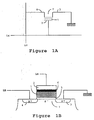
- FIGS. 1A and 1B A conventional memory elementary memory point is shown in FIGS. 1A and 1B, FIG. 1A being a representation in the form of an electrical diagram and FIG. 1B being a schematic sectional view of the elementary memory point.
- FIG. 1A represents a transistor T of a floating gate memory point.
- This transistor has a floating gate 1 and a control gate 2, as well as two regions semiconductors of a first type of conductivity (source 3 and drain 4) separated by a channel region of an opposite type of conductivity covered by the floating gate 1 and the control gate 2.
- the control gate 2 is connected to a word line LM.
- the drain 4 is connected to a bit line LB.
- a voltage is applied to the control gate of the transistor of this memory point that is both higher than the conduction trigger threshold voltage in the non-state programmed and lower than the conduction trigger threshold voltage in the programmed state. If the transistor conducts current when a suitable potential difference is applied between the source and the drain, the memory point is in the non-programmed state. If the transistor does not conduct current, the memory point is in the programmed state.
- Vpp programming potential The potential applied to the control grid when programming the memory point, or Vpp programming potential, is for example 15 volts.
- the drain potential Vcc is then for example 10 volts, and the source potential Vss is for example zero volts, or ground.
- the potential applied to the control grid when reading the memory point is for example 5 volts.
- the drain potential Vcc is then for example 1.5 volts, and the source potential Vss is for example zero volts, or ground.
- FIG. 1B which represents a sectional view of a memory point implanted on a silicon wafer, there is the floating gate 1 and the control gate 2 of the transistor.
- the source 3 and the drain 4 which are two semiconductor regions of a first type of conductivity, for example N+, separated by a channel region 7 of an opposite type of conductivity, for example P ⁇ .
- the floating gate 1 of the transistor is produced by a first level of polycrystalline silicon (poly 1). It is separated from the substrate by a layer of silicon dioxide 5, also called the gate oxide layer.
- silicon dioxide 6 This layer is located between the floating grid 1 and the control grid 2, the latter being produced by a second level of polycrystalline silicon (poly 2) .
- the silicon dioxide layer 6 thus also bears the name of the interpoly oxide layer.
- control gate 2 of the transistor is connected to a word line LM.
- Source 3 is connected to ground, and drain 4 to a bit line LB.
- the drain of a transistor be electrically isolated, by thick silicon oxide (compared to the gate oxide of the transistors), from the drain adjacent transistors of the same word line, failing which it would not be possible to program a particular memory point without programming or deprogramming the others at the same time.
- French patent application 86/12940 has proposed structures where the thick oxide zones and the multiple contacts to the drains or sources are deleted. These structures are called checkerboard structures.
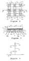
- FIG. 2 represents a top view of nine adjacent memory points in such a checkerboard-type structure.
- the various floating-gate transistors constituting the array of memory points are designated by Tij, where i is a row index and j a column index.
- the transistors T11 to T13 are those of the first row
- the transistors T21 to T23 are those of the second row
- the transistors T31 to T33 are those of the third row.
- the transistors T11 to T31 are those of the first column
- the transistors T12 to T32 are those of the second column
- the transistors T13 to T33 are those of the third column.
- the control gates of the transistors of the same row are all connected to the same word line, LM1 to LM3 for the rows 1 to 3, respectively.
- the word lines are conductors (in practice in polycrystalline silicon) extending in a horizontal direction (direction of the rows).
- Each transistor shares with the two adjacent transistors on the same row a region produced by a diffusion of the first type of conductivity which extends along a column to form a bit line, which is designated by LB1, LB2, LB3 and LB4 for columns 1 to 4, respectively, and by LBj generally speaking.
- These lines LBj can thus act, at the location of the transistors, either as a source office or as a drain office.
- FIG. 3 represents a sectional view along the axis YY ′ of FIG. 2.
- the devices are located on a substrate 10.
- the floating gates 11 of the transistors are produced by a first level of polycrystalline silicon (poly 1) and located between two bit lines.
- the control gates 12 of the transistors are formed by the parts of the word line LM2 located at the location of the transistors.
- the word lines, and thus the control grids of the transistors, are produced by a second level of polycrystalline silicon (poly 2).
- a gate oxide layer 13 is located under the floating gate of the transistors.
- An oxide layer 14 is located between the floating gates of the transistors. Conventionally, a planarization process is used so that the upper surfaces of this layer 14 and of the first level of polycrystalline silicon are at the same level.
- This layer 14 is for example made of tetraethyl ortho silicate or TEOS.
- An interpoly oxide layer 15 covers the floating grids 11 and the oxide layers 14.
- FIG. 4 represents a diagram of the capacities existing at the location of a transistor, for example the transistor T22.
- V F ⁇ V M and which is defined by the ratio between the capacity at the interpoly oxide layer and the sum of all the capacities present.
- the numerical value of the coupling factor is then equal to the ratio between the quantities 0.5 / 20 and 0.5 / 20 + 0.5 / 20, ie only 0.5.
- the present invention provides a new structure which makes it possible to improve the coupling factor and which uses a conventional addressing system.
- this new structure does not have a thick oxide zone, which allows the memory to occupy a reduced bulk.
- the memory is composed of a network of word lines extending in a first direction called row, and bit lines extending in a second direction so-called column, in which each memory point is constituted by a pair of floating gate MOS transistors, the two transistors of this pair having a common drain region constituted by a diffusion of a first type of conductivity which is prolonged according to a column to form a bit line in a substrate of the second type of conductivity, each transistor of a couple has a source region which is constituted by a diffusion of the first type of conductivity extending along a column and which is located on each side , in the direction of the rows, of the common drain region, these source regions all being connected to the same constant potential and, moreover, in which a conductive zone is connected to the floating gates of the two transistors of each pair and is in look of the word line connected to the memory point constituted by the pair of transistors and corresponding, at the location of this pair, to the gri the command line.
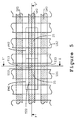
- FIG. 5 represents a top view of an embodiment of the structure according to the present invention. As in the case of FIG. 2, the transistors are arranged in an array of rows and columns.
- control gates of the transistors of row i are still all connected to word lines LMi.
- each memory point is constituted by a couple of transistors.
- Two memory points are for example delimited in the figure by hatched lines and designated by PM1 and PM2.
- a conductive zone 25 is connected to the floating gates of the two transistors of each pair.
- the bit lines LBj are no longer located between each column of transistors, but they are separated by two columns of transistors.
- FIG. 6 makes it possible to examine a memory point along a section YY ′ of FIG. 5.
- This memory point for example the memory point PM1, is also delimited in the figure by hatched lines.
- the devices are located on a substrate 20.
- the common drain region 21 is constituted by a diffusion of a first type of conductivity which extends along a column to form a bit line LB1.
- Each of the two transistors T22 and T23 comprises a source region 22 which is constituted by a diffusion of the first type of conductivity. These diffusions extend along a column and are located on each side, in the direction of the rows, of the common drain region. Each source region is itself shared with a transistor of an adjacent memory point of the same row.
- the floating gates 23 of the transistors are produced by a first level of polycrystalline silicon (poly 1).
- a gate oxide layer 24 is located under the floating gates of the transistors.
- a conductive area 25 is connected to the floating gates of the two transistors T22 and T23. It is produced by a second level of polycrystalline silicon (poly 2).
- This conductive zone 25 is covered on its upper surface by an interpoly oxide layer 26, and it is covered at its two ends, in the direction of the rows, by an oxide zone 27 which is called the corner oxide zone .
- An oxide layer 29 is located between the floating gates of the transistors. As in the case of the checkerboard type structure, a planarization process is used so that the upper surfaces of this layer 29 and of the first level of polycrystalline silicon are at the same level.
- This layer 29 is for example made up of TEOS.
- the word line LM2 covers the whole.
- the interpoly oxide layer 26 and the corner oxide zones 27 make it possible to isolate the conductive zone 25 from the line of word LM2.
- the word line LM2 acts as a control grid 28 at the location of the memory points.
- FIG. 7 shows a sectional view along the axis ZZ 'of Figure 5.
- This figure shows the transistors T13, T23 and T33.
- the transistors each have a floating gate 23 located above the gate oxide layer 24.
- the conductive zone 25 is placed above the floating gates 23 and below the interpoly oxide layer 26. It is observed also the word lines LM1, LM2 and LM3, located above the interpoly oxide layers 26, which act as a control grid 28 at the location of the memory points.
- FIG. 8 represents a diagram of the capacities existing at the location of a memory point of the structure according to the present invention.
- the capacity at the level of the interpoly oxide layer 26 denoted C ′ OI and located between the word line LM2 and the conductive area 25.
- C ′ OG at the level of the layer of gate oxide 24 located between the floating gates 23 and the substrate 20.
- This capacity C ′ OG appears twice in a memory point.
- the numerical value of the coupling factor is then equal to the ratio between the quantities (0.5 + 0.6 + 0.5) / 20 and (0.5 + 0.6 + 0.5) / 20 + 0.5 / 20 + 0.6 / (200 + 20) + 0.5 / 20.
- the coupling factor is then equal to 0.61.
- the structure according to the invention thus makes it possible to improve the coupling factor.
- This structure also has good planarization conditions due to the absence of a thick oxide zone.
- conductive lines (not shown in the figures) made for example of aluminum are each located above a bit line. They are connected to bit lines of other memory blocks, thus making it possible to apply the desired potential to these bit lines and to the drains of the transistors to which the bit lines are connected.
- a conductive line is located between each pair of columns of transistors.
- two columns of transistors separate two adjacent conductive lines. The development of the conducting lines will thus be easier to carry out in the second case.
Landscapes
- Engineering & Computer Science (AREA)
- Microelectronics & Electronic Packaging (AREA)
- Non-Volatile Memory (AREA)
- Semiconductor Memories (AREA)
Claims (7)
- Speicher mit einem Netz aus Wortleitungen (LM1 bis LM3), die sich in einer ersten Richtung in Zeilen erstrecken, und aus Bit-Leitungen (LB1 bis LB4), die sich in einer zweiten Richtung in Spalten erstrecken, wobei:
jeder Speicherpunkt durch ein MOS-Transistorpaar mit schwebendem Gitter gebildet ist,
die beiden Transistoren dieses Paares einen gemeinsamen Drain-Bereich (21) aufweisen, der durch Diffusion eines Materiales eines ersten Leitungstypes, das sich längs einer Spalte erstreckt, gebildet ist, um eine Bit-Leitung in einem Substrat (20) von einem zweiten Leitungstyp zu bilden,
jeder Transistor eines Paares einen Source-Bereich (22) aufweist, der durch Diffusion eines Materiales von einem ersten Leitungstyp gebildet ist, das sich längs einer Spalte erstreckt und längs der Richtung der Zeilen zu beiden Seiten des gemeinsamen Drain-Bereichs gelegen ist, wobei die Source-Bereiche sämtlich an ein gemeinsames konstantes Potential angeschlossen sind,
dadurch gekennzeichnet, daß eine leitende Zone (25) an die schwebenden Gitter (23) der beiden Transistoren jedes Paares angeschlossen ist und in bezug auf eine Wortleitung mit dem Speicherpunkt verbunden ist, der durch das Transistorpaar gebildet wird, wobei diese Wortleitung am Ort des Paares dem Steuergitter (28) entspricht. - Speicher nach Anspruch 1, dadurch gekennzeichnet, daß längs der Richtung der Zeilen eine erste Oxidschicht (29) zwischen den schwebenden Gittern (23) der Transistoren gelegen ist, und daß die Dimensionen der leitenden Zone (25) in Richtung der Zeilen gleich der Summe der zweifachen Dimension der schwebenden Gitter (23) in Zeilenrichtung und der ersten Oxidschicht (29) sind, wobei die Dimensionen der leitenden Zone (25) in Spaltenrichtung gleich derjenigen der Wortreihe und der schwebenden Gitter der Transistoren sind.
- Speicher nach einem der Ansprüche 1 oder 2, dadurch gekennzeichnet, daß die schwebenden Gitter (23) die leitenden Zonen (25) und die Wortleitungen (LMi) jeweils durch ein erstes, zweites bzw. drittes Niveau aus polykristallinem Silizium realisiert sind.
- Speicher nach einem der Ansprüche 1 bis 3, dadurch gekennzeichnet, daß die leitende Zone (25) an ihrer Oberseite durch eine zweite Oxidschicht (26) und an ihren äußeren Rändern in Zeilenrichtung durch eine Kantenoxidzone (27) bedeckt ist, um die Isolierung zwischen der leitenden Zone (25) und der Wortleitung sicherzustellen, die die zweite Oxidschicht (26) und die genannten Kantenoxidzonen (27) bedeckt.
- Verfahren zur Herstellung eines MOS-Speichertyps mit Transistoren mit schwebendem Gitter, die längs Zeilen und Spalten auf einem Substrat eines ersten Leitungstyps angeordnet sind, wobei in dem Speicher jeder Speicherpunkt durch ein Paar von Transistoren gebildet wird, die längs einer Zeile angeordnet sind, mit folgenden Verfahrensschritten:- Abscheiden und Ätzen einer ersten polykristallinen Siliziumschicht, um längs der Spalten Bänder zu bilden, in denen letztlich die schwebenden Gitter (23) der Transistoren angeordnet werden,- Implantieren eines Materials von einem zweiten Leitungstyp, indem die erste Schicht aus polykristallinem Silizium als Maske verwendet wird, um abwechselnd Spalten von Drain-Bereichen (21) und Source-Bereichen (22) dieser Transistoren zu formen,- Formen von Isolierbändern zwischen den unterschiedlichen Bändern der ersten Schicht aus polykristallinem Silizium,dadurch gekennzeichnet, daß darüberhinaus die folgenden Verfahrensschritte vorgesehen sind:- Ablagern einer zweiten Schicht (25) aus polykristallinem Silizium und Isolieren von deren Oberfläche (26),- Ätzen der zweiten Schicht aus polykristallinem Silizium (25), damit sie längs der Spalten die Paare benachbarter Bänder bedeckt, von denen ausgehend die schwebenden Gitter der Transistoren eines Transistorpaares gebildet werden,- Isolieren der freiliegenden seitlichen Bereiche der zweiten Schicht aus polykristallinem Silizium (27),- Abscheiden einer dritten Schicht aus polykristallinem Silizium,- Ätzen der drei Schichten des polykristallinen Siliziums mit einer Maske längs der Zeilen,- Bilden einer Isolierschicht, und- Einrichten von Kontakten zwischen den verbleibenden Bändern der dritten Schicht des polykristallinen Siliziums (Wortleitungen) und den Drain-Spalten (Bit-Leitungen) sowie den Source-Spalten.
- Verfahren zum Herstellen eines Speichers nach Anspruch 5, dadurch gekennzeichnet, daß die Isolierbänder zwischen den Bändern der ersten Schicht aus polykristallinem Silizium durch ein Planarverfahren realisiert werden, das es gestattet, die Oberflächen dieser Schicht (29) und der ersten Schicht aus polykristallinem Silizium auf gleichem Niveau auszuführen.
- Verfahren zum Herstellen eines Speichers nach Anspruch 6, dadurch gekennzeichnet, daß die Isolierbänder aus Tetraethylorthosilikat, d.h. TEOS bestehen.
Applications Claiming Priority (2)
| Application Number | Priority Date | Filing Date | Title |
|---|---|---|---|
| FR8810964A FR2635410B1 (fr) | 1988-08-11 | 1988-08-11 | Memoire de type eprom a haute densite d'integration avec une organisation en damier et un facteur de couplage ameliore et procede de fabrication |
| FR8810964 | 1988-08-11 |
Publications (2)
| Publication Number | Publication Date |
|---|---|
| EP0354859A1 EP0354859A1 (de) | 1990-02-14 |
| EP0354859B1 true EP0354859B1 (de) | 1993-09-22 |
Family
ID=9369373
Family Applications (1)
| Application Number | Title | Priority Date | Filing Date |
|---|---|---|---|
| EP89420288A Expired - Lifetime EP0354859B1 (de) | 1988-08-11 | 1989-07-31 | Hochintegrierte EPROM-Speicheranordnung mit einer quadratischen Gitterorganisation und mit einem verbesserten Kopplungsfaktor |
Country Status (6)
| Country | Link |
|---|---|
| US (1) | US5047362A (de) |
| EP (1) | EP0354859B1 (de) |
| JP (1) | JP2803200B2 (de) |
| KR (1) | KR900004019A (de) |
| DE (1) | DE68909350T2 (de) |
| FR (1) | FR2635410B1 (de) |
Families Citing this family (22)
| Publication number | Priority date | Publication date | Assignee | Title |
|---|---|---|---|---|
| JPH087520B2 (ja) * | 1987-11-10 | 1996-01-29 | コニカ株式会社 | 画像形成装置 |
| US5296396A (en) * | 1988-12-05 | 1994-03-22 | Sgs-Thomson Microelectronics S.R.L. | Matrix of EPROM memory cells with a tablecloth structure having an improved capacitative ratio and a process for its manufacture |
| JP2685966B2 (ja) * | 1990-06-22 | 1997-12-08 | 株式会社東芝 | 不揮発性半導体記憶装置 |
| US5270240A (en) * | 1991-07-10 | 1993-12-14 | Micron Semiconductor, Inc. | Four poly EPROM process and structure comprising a conductive source line structure and self-aligned polycrystalline silicon digit lines |
| US5149665A (en) * | 1991-07-10 | 1992-09-22 | Micron Technology, Inc. | Conductive source line for high density programmable read-only memory applications |
| US6780740B1 (en) * | 1993-07-27 | 2004-08-24 | Micron Technology, Inc. | Method for fabricating a floating gate semiconductor device |
| US6281103B1 (en) | 1993-07-27 | 2001-08-28 | Micron Technology, Inc. | Method for fabricating gate semiconductor |
| US5767005A (en) | 1993-07-27 | 1998-06-16 | Micron Technology, Inc. | Method for fabricating a flash EEPROM |
| KR0135234B1 (ko) * | 1994-08-09 | 1998-04-22 | 김주용 | 비휘발성 기억소자 제조방법 |
| US5622881A (en) * | 1994-10-06 | 1997-04-22 | International Business Machines Corporation | Packing density for flash memories |
| KR100192430B1 (ko) * | 1995-08-21 | 1999-06-15 | 구본준 | 비휘발성 메모리 및 이 비휘발성 메모리를 프로그램하는 방법 |
| KR0172831B1 (ko) * | 1995-09-18 | 1999-03-30 | 문정환 | 비휘발성 메모리를 프로그램하는 방법 |
| KR100192476B1 (ko) * | 1996-06-26 | 1999-06-15 | 구본준 | 다중 비트 메모리 셀의 데이타 센싱장치 및 방법 |
| KR100226746B1 (ko) * | 1996-12-30 | 1999-10-15 | 구본준 | 다중비트셀의데이타센싱장치및방법 |
| US5933735A (en) * | 1997-01-16 | 1999-08-03 | United Microelectronics Corp. | Semiconductor read-only memory device and method of fabricating the same |
| KR100244268B1 (ko) * | 1997-04-02 | 2000-02-01 | 김영환 | 비휘발성 메모리 소자 및 제조 방법 |
| KR100232200B1 (ko) * | 1997-05-26 | 1999-12-01 | 김영환 | 비휘발성 메모리 소자 및 제조 방법 |
| KR100316709B1 (ko) * | 1998-07-13 | 2001-12-12 | 윤종용 | 불휘발성 메모리 장치 제조 방법 |
| FR2800200B1 (fr) * | 1999-10-21 | 2002-01-04 | St Microelectronics Sa | Procede de fabrication de points memoire eeprom |
| US6512263B1 (en) | 2000-09-22 | 2003-01-28 | Sandisk Corporation | Non-volatile memory cell array having discontinuous source and drain diffusions contacted by continuous bit line conductors and methods of forming |
| JP2003031702A (ja) * | 2001-07-16 | 2003-01-31 | Mitsubishi Electric Corp | 不揮発性半導体記憶装置およびその製造方法 |
| KR100851553B1 (ko) * | 2006-10-02 | 2008-08-11 | 삼성전자주식회사 | 반도체 소자 및 그 구동방법 |
Family Cites Families (13)
| Publication number | Priority date | Publication date | Assignee | Title |
|---|---|---|---|---|
| US3893152A (en) * | 1973-07-25 | 1975-07-01 | Hung Chang Lin | Metal nitride oxide semiconductor integrated circuit structure |
| US3984822A (en) * | 1974-12-30 | 1976-10-05 | Intel Corporation | Double polycrystalline silicon gate memory device |
| JPS5550667A (en) * | 1978-10-09 | 1980-04-12 | Fujitsu Ltd | Method of fabricating double gate mos-type integrated circuit |
| US4267632A (en) * | 1979-10-19 | 1981-05-19 | Intel Corporation | Process for fabricating a high density electrically programmable memory array |
| JPS5929155B2 (ja) * | 1979-11-12 | 1984-07-18 | 富士通株式会社 | 半導体記憶装置 |
| JPS5878467A (ja) * | 1981-11-05 | 1983-05-12 | Seiko Instr & Electronics Ltd | 不揮発性半導体メモリ |
| US4527258A (en) * | 1982-09-30 | 1985-07-02 | Mostek Corporation | E2 PROM having bulk storage |
| FR2537779B1 (fr) * | 1982-12-10 | 1986-03-14 | Commissariat Energie Atomique | Procede de positionnement d'un trou de contact electrique entre deux lignes d'interconnexion d'un circuit integre |
| US4713142A (en) * | 1985-05-01 | 1987-12-15 | Texas Instruments Incorporated | Method for fabricating EPROM array |
| IT1191755B (it) * | 1986-04-29 | 1988-03-23 | Sgs Microelettronica Spa | Processo di fabbricazione per celle eprom con dielettrico ossido-nitruro-ossido |
| FR2603128B1 (fr) * | 1986-08-21 | 1988-11-10 | Commissariat Energie Atomique | Cellule de memoire eprom et son procede de fabrication |
| FR2604022B1 (fr) * | 1986-09-16 | 1992-09-11 | Eurotechnique Sa | Memoire non volatile a grille flottante sans oxyde epais |
| FR2618011B1 (fr) * | 1987-07-10 | 1992-09-18 | Commissariat Energie Atomique | Procede de fabrication d'une cellule de memoire |
-
1988
- 1988-08-11 FR FR8810964A patent/FR2635410B1/fr not_active Expired - Lifetime
-
1989
- 1989-07-31 EP EP89420288A patent/EP0354859B1/de not_active Expired - Lifetime
- 1989-07-31 DE DE89420288T patent/DE68909350T2/de not_active Expired - Fee Related
- 1989-08-09 KR KR1019890011345A patent/KR900004019A/ko not_active Withdrawn
- 1989-08-11 JP JP1207053A patent/JP2803200B2/ja not_active Expired - Lifetime
- 1989-08-11 US US07/392,699 patent/US5047362A/en not_active Expired - Lifetime
Also Published As
| Publication number | Publication date |
|---|---|
| JPH031575A (ja) | 1991-01-08 |
| EP0354859A1 (de) | 1990-02-14 |
| FR2635410B1 (fr) | 1991-08-02 |
| DE68909350D1 (de) | 1993-10-28 |
| DE68909350T2 (de) | 1994-04-21 |
| KR900004019A (ko) | 1990-03-27 |
| US5047362A (en) | 1991-09-10 |
| FR2635410A1 (fr) | 1990-02-16 |
| JP2803200B2 (ja) | 1998-09-24 |
Similar Documents
| Publication | Publication Date | Title |
|---|---|---|
| EP0354859B1 (de) | Hochintegrierte EPROM-Speicheranordnung mit einer quadratischen Gitterorganisation und mit einem verbesserten Kopplungsfaktor | |
| KR100219519B1 (ko) | 페로일렉트릭 플로팅 게이트 램을 구비하는 반도체 메모리 디바이스 및 그 제조방법 | |
| EP0780902B1 (de) | Nichtflüchtige Halbleiteranordnung und Verfahren zur Herstellung | |
| FR2879800A1 (fr) | Dispositif a memoire integree et procede | |
| US20190074286A1 (en) | Method of reducing charge loss in non-volatile memories | |
| US20070029618A1 (en) | Dual-gate device and method | |
| JPH1093083A (ja) | 半導体装置の製造方法 | |
| EP0648375B1 (de) | Flash-eeprom-speicher mit drei gateelektroden und sein herstellungsverfahren. | |
| EP1495496A1 (de) | Elektrisch löschbare und programmiebare nichtflüchtige halbleiterspeicheranordnung mit einschichtigem gatematerial und entsprechende speicherfläche | |
| FR2987696A1 (fr) | Procede de lecture ecriture de cellules memoire non volatiles | |
| FR2987700A1 (fr) | Memoire non volatile comprenant des mini caissons a potentiel flottant | |
| EP0354858B1 (de) | Hochintegrierte EPROM-Speicheranordnung mit einem grossen Kopplungsfaktor | |
| EP0356346B1 (de) | Hochintegrierte EPROM-Speicheranordnung | |
| FR3080949A1 (fr) | Dispositif de memoire non volatile du type a piegeage de charges et procede de fabrication | |
| US8300448B2 (en) | Semiconductor storage device, memory cell array, and a fabrication method and drive method of a semiconductor storage device | |
| EP0282520B1 (de) | Nichtflüchtiger speicher mit isoliertem gate ohne dickes oxid | |
| WO2009147347A1 (fr) | Memoire a structure du type eeprom et a lecture seule | |
| EP0354860A1 (de) | Hochintegrierte EPROM-Speicheranordnung mit einer quadratischen Gitterorganisation, einem verbesserten Kopplungsfaktor und einer Redundanzmöglichkeit | |
| CN110364198A (zh) | 编码型快闪存储器及其制造方法 | |
| US20050142743A1 (en) | Flash memory cell and method for manufacturing the same | |
| FR3054723A1 (fr) | Cellule-memoire eeprom compacte avec zone d'injection tunnel reduite | |
| FR2638021A1 (fr) | Memoire eprom de type damier et procede de fabrication | |
| FR3144402A1 (fr) | Circuit électronique comprenant une cellule de transistors | |
| FR3164829A1 (fr) | Réduction de la consommation d’énergie de programmation ou d’effacement d’une cellule mémoire à grille divisée, cellule mémoire et procédé de fabrication | |
| JP4574912B2 (ja) | 半導体記憶装置の形成方法 |
Legal Events
| Date | Code | Title | Description |
|---|---|---|---|
| PUAI | Public reference made under article 153(3) epc to a published international application that has entered the european phase |
Free format text: ORIGINAL CODE: 0009012 |
|
| AK | Designated contracting states |
Kind code of ref document: A1 Designated state(s): DE FR GB IT NL |
|
| 17P | Request for examination filed |
Effective date: 19900803 |
|
| 17Q | First examination report despatched |
Effective date: 19921211 |
|
| GRAA | (expected) grant |
Free format text: ORIGINAL CODE: 0009210 |
|
| AK | Designated contracting states |
Kind code of ref document: B1 Designated state(s): DE FR GB IT NL |
|
| PG25 | Lapsed in a contracting state [announced via postgrant information from national office to epo] |
Ref country code: NL Effective date: 19930922 |
|
| REF | Corresponds to: |
Ref document number: 68909350 Country of ref document: DE Date of ref document: 19931028 |
|
| GBT | Gb: translation of ep patent filed (gb section 77(6)(a)/1977) |
Effective date: 19931012 |
|
| ITF | It: translation for a ep patent filed | ||
| NLV1 | Nl: lapsed or annulled due to failure to fulfill the requirements of art. 29p and 29m of the patents act | ||
| PLBE | No opposition filed within time limit |
Free format text: ORIGINAL CODE: 0009261 |
|
| STAA | Information on the status of an ep patent application or granted ep patent |
Free format text: STATUS: NO OPPOSITION FILED WITHIN TIME LIMIT |
|
| 26N | No opposition filed | ||
| REG | Reference to a national code |
Ref country code: FR Ref legal event code: D6 |
|
| PGFP | Annual fee paid to national office [announced via postgrant information from national office to epo] |
Ref country code: FR Payment date: 20010712 Year of fee payment: 13 |
|
| REG | Reference to a national code |
Ref country code: GB Ref legal event code: IF02 |
|
| PGFP | Annual fee paid to national office [announced via postgrant information from national office to epo] |
Ref country code: GB Payment date: 20020731 Year of fee payment: 14 |
|
| PGFP | Annual fee paid to national office [announced via postgrant information from national office to epo] |
Ref country code: DE Payment date: 20020807 Year of fee payment: 14 |
|
| PG25 | Lapsed in a contracting state [announced via postgrant information from national office to epo] |
Ref country code: FR Free format text: LAPSE BECAUSE OF NON-PAYMENT OF DUE FEES Effective date: 20030331 |
|
| REG | Reference to a national code |
Ref country code: FR Ref legal event code: ST |
|
| PG25 | Lapsed in a contracting state [announced via postgrant information from national office to epo] |
Ref country code: GB Free format text: LAPSE BECAUSE OF NON-PAYMENT OF DUE FEES Effective date: 20030731 |
|
| PG25 | Lapsed in a contracting state [announced via postgrant information from national office to epo] |
Ref country code: DE Free format text: LAPSE BECAUSE OF NON-PAYMENT OF DUE FEES Effective date: 20040203 |
|
| GBPC | Gb: european patent ceased through non-payment of renewal fee |
Effective date: 20030731 |
|
| PG25 | Lapsed in a contracting state [announced via postgrant information from national office to epo] |
Ref country code: IT Free format text: LAPSE BECAUSE OF NON-PAYMENT OF DUE FEES;WARNING: LAPSES OF ITALIAN PATENTS WITH EFFECTIVE DATE BEFORE 2007 MAY HAVE OCCURRED AT ANY TIME BEFORE 2007. THE CORRECT EFFECTIVE DATE MAY BE DIFFERENT FROM THE ONE RECORDED. Effective date: 20050731 |