EP0354858B1 - Hochintegrierte EPROM-Speicheranordnung mit einem grossen Kopplungsfaktor - Google Patents
Hochintegrierte EPROM-Speicheranordnung mit einem grossen Kopplungsfaktor Download PDFInfo
- Publication number
- EP0354858B1 EP0354858B1 EP89420287A EP89420287A EP0354858B1 EP 0354858 B1 EP0354858 B1 EP 0354858B1 EP 89420287 A EP89420287 A EP 89420287A EP 89420287 A EP89420287 A EP 89420287A EP 0354858 B1 EP0354858 B1 EP 0354858B1
- Authority
- EP
- European Patent Office
- Prior art keywords
- transistors
- floating gate
- level
- transistor
- columns
- Prior art date
- Legal status (The legal status is an assumption and is not a legal conclusion. Google has not performed a legal analysis and makes no representation as to the accuracy of the status listed.)
- Expired - Lifetime
Links
Images






Classifications
-
- H—ELECTRICITY
- H10—SEMICONDUCTOR DEVICES; ELECTRIC SOLID-STATE DEVICES NOT OTHERWISE PROVIDED FOR
- H10B—ELECTRONIC MEMORY DEVICES
- H10B41/00—Electrically erasable-and-programmable ROM [EEPROM] devices comprising floating gates
- H10B41/10—Electrically erasable-and-programmable ROM [EEPROM] devices comprising floating gates characterised by the top-view layout
-
- H—ELECTRICITY
- H10—SEMICONDUCTOR DEVICES; ELECTRIC SOLID-STATE DEVICES NOT OTHERWISE PROVIDED FOR
- H10B—ELECTRONIC MEMORY DEVICES
- H10B41/00—Electrically erasable-and-programmable ROM [EEPROM] devices comprising floating gates
-
- H—ELECTRICITY
- H10—SEMICONDUCTOR DEVICES; ELECTRIC SOLID-STATE DEVICES NOT OTHERWISE PROVIDED FOR
- H10B—ELECTRONIC MEMORY DEVICES
- H10B69/00—Erasable-and-programmable ROM [EPROM] devices not provided for in groups H10B41/00 - H10B63/00, e.g. ultraviolet erasable-and-programmable ROM [UVEPROM] devices
-
- H—ELECTRICITY
- H10—SEMICONDUCTOR DEVICES; ELECTRIC SOLID-STATE DEVICES NOT OTHERWISE PROVIDED FOR
- H10D—INORGANIC ELECTRIC SEMICONDUCTOR DEVICES
- H10D30/00—Field-effect transistors [FET]
- H10D30/60—Insulated-gate field-effect transistors [IGFET]
- H10D30/68—Floating-gate IGFETs
- H10D30/681—Floating-gate IGFETs having only two programming levels
- H10D30/684—Floating-gate IGFETs having only two programming levels programmed by hot carrier injection
- H10D30/685—Floating-gate IGFETs having only two programming levels programmed by hot carrier injection from the channel
-
- H—ELECTRICITY
- H10—SEMICONDUCTOR DEVICES; ELECTRIC SOLID-STATE DEVICES NOT OTHERWISE PROVIDED FOR
- H10D—INORGANIC ELECTRIC SEMICONDUCTOR DEVICES
- H10D64/00—Electrodes of devices having potential barriers
- H10D64/20—Electrodes characterised by their shapes, relative sizes or dispositions
- H10D64/27—Electrodes not carrying the current to be rectified, amplified, oscillated or switched, e.g. gates
- H10D64/311—Gate electrodes for field-effect devices
- H10D64/411—Gate electrodes for field-effect devices for FETs
- H10D64/511—Gate electrodes for field-effect devices for FETs for IGFETs
- H10D64/517—Gate electrodes for field-effect devices for FETs for IGFETs characterised by the conducting layers
- H10D64/518—Gate electrodes for field-effect devices for FETs for IGFETs characterised by the conducting layers characterised by their lengths or sectional shapes
-
- H—ELECTRICITY
- H10—SEMICONDUCTOR DEVICES; ELECTRIC SOLID-STATE DEVICES NOT OTHERWISE PROVIDED FOR
- H10D—INORGANIC ELECTRIC SEMICONDUCTOR DEVICES
- H10D64/00—Electrodes of devices having potential barriers
- H10D64/20—Electrodes characterised by their shapes, relative sizes or dispositions
- H10D64/27—Electrodes not carrying the current to be rectified, amplified, oscillated or switched, e.g. gates
- H10D64/311—Gate electrodes for field-effect devices
- H10D64/411—Gate electrodes for field-effect devices for FETs
- H10D64/511—Gate electrodes for field-effect devices for FETs for IGFETs
- H10D64/517—Gate electrodes for field-effect devices for FETs for IGFETs characterised by the conducting layers
- H10D64/519—Gate electrodes for field-effect devices for FETs for IGFETs characterised by the conducting layers characterised by their top-view geometrical layouts
Definitions
- the present invention relates to semiconductor memories, and more particularly to electrically programmable non-volatile memories, more commonly called EPROM memories; the manufacture of floating gate memories is more specifically concerned.
- the thick oxide which isolates two adjacent points takes up a lot of space, especially when it is produced by the so-called localized oxidation technique.
- the present invention proposes a new memory architecture which makes it possible to provide such a thick oxide zone only for both transistors connected to the same line of word.
- the new architecture proposed makes it possible to avoid the presence of contacts on the bit lines between the cells.
- the memory is composed of a network of word lines extending in a first direction, called a row direction, connecting control gates of floating-gate transistors, and bit lines extending in a second direction, called column direction, connecting drains of floating gate transistors.
- a respective conductive area of dimensions greater than those of the floating gate of the transistors in a horizontal plane, is connected to the floating gate of each transistor of the memory, while being located opposite the corresponding word line from which it is separated. by an insulation layer.
- FIG. 1A represents a transistor T of a floating gate memory point.
- This transistor has a floating gate 1 and a control gate 2, as well as two semiconductor regions of a first type of conductivity (source 3 and drain 4) separated by a channel region of an opposite type of conductivity covered by the gate. floating 1 and the control grid 2.
- the control gate 2 is connected to a word line LM.
- the drain 4 is connected to a bit line LB.
- a voltage is applied to the control gate of the transistor of this memory point that is both greater than the conduction trigger threshold voltage in the non-state programmed and lower than the conduction trigger threshold voltage in the programmed state. If the transistor conducts current when a suitable potential difference is applied between the source and the drain, the memory point is in the non-programmed state. If the transistor does not conduct current, the memory point is in the programmed state.
- Vpp programming potential The potential applied to the control grid when programming the memory point, or Vpp programming potential, is for example 15 volts.
- the drain potential Vcc is then by example of 10 volts, and the source potential Vss is for example zero volts, or ground.
- the potential applied to the control grid when reading the memory point is for example 5 volts.
- the drain potential Vcc is then for example 1.5 volts, and the source potential Vss is for example zero volts, or ground.
- FIG. 1B which represents a sectional view of a memory point implanted on a silicon wafer, there is the floating gate 1 and the control gate 2 of the transistor.
- the source 3 and the drain 4 which are two semiconductor regions of a first type of conductivity, for example N+, separated by a channel region 7 of an opposite type of conductivity, for example P ⁇ .
- the floating gate 1 of the transistor is produced by a first level of polycrystalline silicon (poly 1). It is separated from the substrate by a layer of silicon dioxide 5, also called the gate oxide layer.
- silicon dioxide 6 This layer is located between the floating grid 1 and the control grid 2, the latter being produced by a second level of polycrystalline silicon (poly 2) .
- the silicon dioxide layer 6 thus also bears the name of the interpoly oxide layer.
- control gate 2 of the transistor is connected to a word line LM.
- Source 3 is connected to ground, and drain 4 to a bit line LB.
- FIG. 2 represents a top view of a conventional mode of implantation of six adjacent memory points on a silicon wafer.
- the various floating-gate transistors constituting the array of memory points are designated by Tij, where i is a row index and j a column index.
- the transistors T11 to T13 are those of the first row
- the transistors T21 to T23 are those of the second row.
- the transistors T11 and T21 are those of the first column
- the transistors T12 and T22 are those of the second column
- the transistors T13 and T23 are those of the third column.
- the control gates of the transistors of the same row are all connected to the same word line, LM1 and LM2 for the rows 1 and 2, respectively.
- the drains of the transistors of the same column are all connected to the same bit line, LB1 to LB3 for columns 1 to 3, respectively.
- the word lines are conductors (in practice in polycrystalline silicon) extending in a horizontal direction (direction of the rows).
- Bit lines are conductors extending in a vertical direction (direction of columns).
- bit lines pass over the transistors Tij forming the memory points.
- the floating gates 1 of the transistors are located between the drains 4 and the sources 3.
- the sources of the transistors of the same row are all connected to a common line L.
- All the common lines L are connected by a contact 12 to a conductive line A which, being itself at the source potential Vss, makes it possible to apply the voltage Vss to the sources of the transistors.
- An isolation zone 13 is located between each common line L and between each column of transistors.
- the isolation zone is made of thick silicon oxide (compared to the gate oxide).
- the floating gate 1 of the transistors overflows onto the isolation zone.
- FIG. 3 is a section along the axis YY ′ in FIG. 2.
- the floating grid 1 runs along the row of transistors and acts as a control grid 2 at the location of the transistors.
- the word line LM1 is covered by an insulating layer 14.
- This insulating layer 14 is for example made of silicon oxide doped with boron and phosphorus (BPSG) which makes it possible to obtain good creep at low temperatures (around 850 at 950 ° C).
- BPSG boron and phosphorus
- the bit lines LB2 and LB3 are located on the insulating layer 14, above the transistors T12 and T13 respectively.
- Figure 4 shows a sectional view along the axis ZZ ′ of Figure 2, the two transistors T12 and T22.
- each transistor comprises a source region 3 and a drain region 4 separated by a channel region 7, as well as the superposition of the layers forming the gate oxide 5, the floating gate 1 , the interpoly oxide 6 and the control grid 2.
- the control gates of the transistors are covered by the insulating layer 14.
- the bit line LB2 is connected to the drains of the two transistors by the contact 11.
- bit line LB2 when it comes into contact with the drain regions of the transistors T12 and T22. All the bit lines, made for example of aluminum, will be subjected to walking passages every two rows of transistors, which constitutes a significant risk of breakage of the aluminum lines.
- the present invention provides an architecture which avoids these drawbacks and has the advantage of having a high coupling factor.
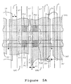
- FIG. 5A represents the structure at an intermediate stage of manufacture after deposition of two levels of polycrystalline silicon.
- FIG. 5B represents the structure after deposition of a third level of polycrystalline silicon and etching of the various levels of polycrystalline silicon.
- the transistors are always arranged in an array of rows and columns, the transistors of the first row still being designated by T11 and T12, those of the second row by T21 and T22, and the transistor Tij more generally designating the transistor which is at the crossroads of row i and column j.
- the control gates of the transistors in row i are still all connected to a general direction conductor horizontal called word line LMi.
- the word lines are also conductors (in practice in polycrystalline silicon) extending in a horizontal direction (direction of the rows).
- the bit lines LBj consist of regions of the substrate of a first type of conductivity, for example n+. Each bit line acts directly as a drain 21 at the location of each transistor. There is therefore no longer any need to provide a contact every two rows of transistors on each of the bit lines (contacts designated by 11 in FIG. 2).
- Lines with constant potential, conductive, of general vertical direction, are inserted every second time between two bit lines, they are designated by B.
- These lines with constant potential B are constituted by regions of the first type of conductivity, such as bit lines LBj, and they act as sources 22 at the locations of the transistors.
- isolation zones 24 which are in principle made of thick silicon oxide.
- the floating gates 23 of the transistors are produced by a first level of polycrystalline silicon (poly 1) and located on each side of each line with constant potential B.
- Zones E produced by the first level of polycrystalline silicon, cover the edges adjacent to the columns of transistors of the isolation zones (24) and extend beyond it by a length 1.
- the floating gates 23 are still part, at the manufacturing stage represented in FIG. 5A, strips of poly 1 designated by P1 which extend in the direction of the columns.
- the strips of poly 1 P1 have been etched and the floating grids 23 are formed definitively by rectangles of poly 1.
- a layer 35 ′ produced by the second level of polycrystalline silicon (poly 2) is connected to each strip of poly 1 P1 extending in the direction of the columns.
- the layers 35 ′ have a greater width than that of the strips of poly 1 P1.
- zones 35 formed by the poly 2 are observed which are the remaining part of the layer 35 ′ after etching of the latter.
- Each zone 35 is connected to a floating grid 23.
- the dimensions along the direction of the columns of the zones 35 are identical to those of the floating grids 23, and the dimensions along the direction of the rows of the zones 35 are greater than those of the floating grids 23.
- the zones 35 extend beyond the floating grids 23, on the side of the source regions 22, of a length a, and the zones 35 pass over the zones E and extend beyond it by a length b.
- the word lines LM1 and LM2 are formed by a third level of polycrystalline silicon (poly 3).
- the current in the channel will flow in the horizontal direction, or direction of the word lines, and thus, the transistor will have a channel region oriented in the same direction. than the word lines.
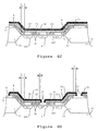
- FIGS. 6A to 6G represent sectional views along the axis YY ′ of FIGS. 5A or 5B, they each correspond to a step in the process for manufacturing the structure according to the invention carried out in a silicon substrate 20.
- FIG. 6A represents the structure at a preliminary stage after completion of the thick oxide zones 24 and of the gate oxide layers 27, after deposition and etching of the first level of polycrystalline silicon to form on the one hand strips of poly 1 P1 in which the floating gates 23 of the transistors and on the other hand the zones E will be defined subsequently.
- the thick oxide zones 24 have for example a thickness of 700 nm and the gate oxide layers 27 have for example a thickness of 20 nm.
- P-type regions 18 are located under the thick oxide zones 24. These regions 18 are commonly called channel stop regions. Also shown are doped regions 19 located under the gate oxide layers 27 to define the triggering threshold of the transistors of the memory.
- FIG. 6B represents the structure at an intermediate stage after formation of heavily doped N+ type regions which constitute on the one hand the bit lines LBj and on the other hand the lines with constant potential B. These regions are produced by implantation d 'arsenic.
- FIG. 6B also shows the structure after deposition of an insulation layer 36 between the different poly 1 zones. Conventionally, a planarization process is used so that the upper surfaces of this layer 36 and of the first silicon level polycrystalline are at the same level.
- This layer 36 consists of silicon oxide obtained for example by vapor deposition from a TEOS source (tetraethyl ortho silicate).
- FIG. 6C represents the structure at an intermediate stage after deposition of the second level of polycrystalline silicon 35 ′ and production of an insulating layer 28, which is commonly called an interpoly oxide layer, and which is formed in this structure by a stack of three layers silicon oxide / silicon nitride / silicon oxide called ONO.
- FIG. 6D represents the structure at an intermediate stage after etching of the interpoly oxide layer 28 and of the second level of polycrystalline silicon 35 ′ at the level of a part of the insulation layer 36 located at the location of the lines to constant potential B and on the other hand of the insulating layer 36 situated above the thick oxide zones 24.
- FIG. 6D also shows the structure after completion of an oxide zone 37, called the corner oxide zone, at each end, in the direction of the rows, of the layers 35 ′ defined by the etching.
- FIG. 6E represents the structure at an intermediate stage after deposition of the third level of polycrystalline silicon (poly 3) from which the word lines LMi are formed, and etching of the poly 3, of the ONO 28 interpoly oxide layer, of the poly 2 and poly 1 which makes it possible to define the word lines LMi formed in the poly 3, the zones 35 formed in the layers 35 ′, and the floating grids 23 formed in the strips of poly 1 P1.
- poly 3 the third level of polycrystalline silicon
- Figure 7 shows a sectional view along the axis ZZ ′ of Figure 5B.
- FIG. 6F represents the structure at an intermediate stage after deposition of an insulating layer 29.
- This layer 29 is for example made of silicon oxide doped with boron and phosphorus (BPSG).
- FIG. 6G represents the structure in the final step after production of conductive lines 30 situated on the insulating layer 29 and constituted for example of aluminum, each being placed above a bit line.
- bit lines of other memory blocks are connected to bit lines of other memory blocks (indeed, memory points are usually grouped into blocks occupying a certain number of rows and columns) thus making it possible to apply the desired potential to these bit lines and to the drains of the transistors to which the bit lines are connected.
- the conductive lines 30 extend over a flat surface, which makes it possible to avoid the problems due to the passage of step to which the aluminum lines are subjected in the classic configuration.
- the space existing between the pairs of conductive lines 30 is greater than the space existing between the pairs of aluminum lines constituting the bit lines in the conventional configuration.
- FIG. 7 which represents a sectional view along the axis ZZ ′ of FIG. 5B, we see the floating gates 23 of the transistors, these floating gates being located above the gate oxide layer 27. On also observes the zones 35 formed by the second level of polycrystalline silicon, and the ONO interpoly oxide layers 28 located above the zones 35. We also observe the two word lines LM1 and LM2 which act as control grids 25 at the location of the transistors.
- FIG. 8A represents a diagram of the capacities existing at the location of a transistor in the case where the architecture does not have a zone 35 connected to the floating gate 23 of the transistor
- FIG. 8B represents a diagram of the capacities existing at the location of a transistor in the case of the architecture according to the invention.
- V F ⁇ V M and which is defined by the ratio between the capacity at the interpoly oxide layer and the sum of all the capacities present.
- a capacitance again appears at the level of the interpoly oxide layer 28 denoted C ′ OI and situated between the line of word LM2 and zone 35.
- C ′ OI a capacity at the level of the gate oxide layer 27 denoted C ′ OG .
- C OA a capacity corresponding to the zone portion 35 which extends beyond the floating grid 23 by a length a in the direction of the rows, a capacity C OD at the level of the oxide part of TEOS type.
- a capacity C BO corresponding to the part of the zone E which extends beyond a length 1 beyond the isolation zones 24, at the level of the part of the oxide layer grid 27 located between the part of zone E which projects and the substrate 20, a capacitance C ZI corresponding to the part of zone E situated above the isolation zone 24, at the level of this isolation zone 24, and a capacitance C OB corresponding to the overflow of the zone 35 beyond the zone E of a length b, at the level of the TEOS type oxide part separating two zones E and of the isolation zone 24.
- the coupling factor is then substantially equal to 0.70.
- This architecture by the presence of the zone 35 connected to the floating gate 23 of the transistor, thus makes it possible to obtain a significantly improved coupling factor.
- the gate oxide layer which is designated in FIG. 9 by 27 ′, is very thin compared to the usual values, it has for example a thickness of the around 10 nm.
- the constant potential line B ′ consists of two parts doped to a different degree. There is a first heavily doped part 22-1, the doping being for example N+; this first part is located in a box 22-2 of the same type of conductivity with low doping, the doping then being for example N ⁇ .
- the constant potential line B ′ still acts as a source 22 ′ at the location of the transistors.
- This new arrangement allows, if a sufficiently high voltage is applied to the source 22 ′, the transfer by tunnel effect of charge carriers, trapped during a programming operation in the floating gate of the transistors, from the floating gate to the part from the high doping source. This transfer is made possible by the great thinness of the gate oxide layer, it is represented by the arrow in FIG. 9.
- the presence of the second lightly doped part makes it possible to increase the breakdown voltage between the source and the substrate.
- the advantage presented by the architecture according to the invention lies in the fact that the regions of thin oxide through which the charge carriers pass are never in contact with or near a zone of thick oxide.
Landscapes
- Semiconductor Memories (AREA)
- Non-Volatile Memory (AREA)
Claims (9)
- Speicher mit einem Netz aus Wortlinien (LM1, LM2), die sich in einer ersten Richtung, der sogenannten Zeilenrichtung erstrecken und die Steuergitter (25) von Transistoren mit schwebendem Gitter verbinden, und aus Bitlinien (LB1, LB2), die sich in einer zweiten Richtung, der sogenannten Spaltenrichtung erstrecken und die Drainelektroden der Transistoren mit schwebendem Gitter verbinden, dadurch gekennzeichnet, daß eine entsprechende leitende Zone (35), deren Dimensionen in einer horizontalen Ebene größer sind als diejenigen des schwebenden Gitters (23) der Transistoren, mit dem schwebenden Gitter eines Jeden Transistors des Speichers verbunden und längs der entsprechenden Wortlinie ausgerichtet ist, von der sie durch eine Isolationsschicht (28) getrennt ist.
- Speicher nach Anspruch 1, dadurch gekennzeichnet, daß:
eine Linie mit konstantem Potential (B), die sich längs einer Spalte erstreckt und durch eine Diffusion eines ersten Leitungstypes zur Verbindung der Sourceelektroden der Transistoren gebildet ist, Jeweils zwischen einem Paar aus zwei Bitlinien angeordnet ist, wobei alle Linien mit konstantem Potential auf dem gleichen Potential liegen,
jeder Transistor ein schwebendes Gitter (23), das im wesentlichen durch ein leitendes Rechteck gebildet ist, und ein Steuergitter (25) aufweist, das durch den Teil der Wortlinie gebildet ist, die im wesentlichen am Ort des schwebenden Gitters des Transistors gelegen ist,
die leitende Zone (35) durch ein Rechteck gebildet ist, dessen Dimensionen in Zeilenrichtung größer als diejenigen des schwebenden Gitters (23) sind,
eine Isolationszone (24), die sich längs einer Spalte erstreckt, jeweils auf der Seite einer jeden Bitlinie angeordnet ist, die der Linie mit konstantem Potential gegenüberliegt. - Speicher nach Anspruch 2, dadurch gekennzeichnet, daß eine zusätzliche leitende Zone (E) die Längsränder der Isolationszonen (24) überdeckt, wobei diese zusätzliche Zone (E) aus dem gleichen Material aufgebaut ist, aus dem die schwebenden Gitter (23) der Transistoren bestehen.
- Speicher nach einem der Ansprüche 2 oder 3, dadurch gekennzeichnet, daß in einem Transistor die leitende Zone (35), die in Spaltenrichtung im wesentlichen die gleichen Dimensionen wie die Wortlinie und das schwebende Gitter hat, das schwebende Gitter in Zeilenrichtung beidseitig überragt, wobei sie über das schwebende Gitter mit einer ersten Länge (a) auf der Seite der Linie mit konstantem Potential herausragt und über der Isolationszone (24) und der zusätzlichen Zone (E), die sich an den Transistor anschließen, ansteigt und dabei über die zusätzliche Zone (E) um eine zweite Länge (b) herausragt.
- Speicher nach einem der Ansprüche 1 bis 4, dadurch gekennzeichnet, daß die schwebenden Gitter (23), die leitenden Zonen (35) und die Wortlinien (LMi) durch ein erstes, zweites bzw. drittes Niveau aus polykristallinem Silizium gebildet sind.
- Speicher nach einem der Ansprüche 1 bis 5, dadurch gekennzeichnet, daß die Isolationszonen (24) aus einem dicken Siliziumoxid gebildet sind.
- Verfahren zur Herstellung eines Speichers vom Typ MOS mit Transistoren mit schwebendem Gitter, die auf einem Substrat eines ersten Leitungstyps längs Zeilen und Spalten angeordnet sind, mit folgenden Schritten:- Ausbilden von Zonen eines dicken Oxids (24) längs der Spalten,- Aufbringen und Ätzen eines ersten Niveaus aus polykristallinem Silizium, um längs der Spalten einerseits zwei erste benachbarte Streifen zwischen jedem Paar von Spalten des dicken Oxids und andererseits zwei zweite Streifen auszubilden, von denen jeder den Bereich innerhalb dieses Paares und einen Bereich der entsprechenden dicken Oxidzone überdeckt,- Implantieren eines zweiten Leitungstypes, wobei das erste Niveau aus polykristallinem Silizium als Maske verwendet wird,- Ausbilden einer Isolationsschicht (36) zwischen den unterschiedlichen Zonen des ersten Niveaus aus polykristallinem Silizium,
dadurch gekennzeichnet, daß noch die folgenden Schritte vorliegen:- Aufbringen eines zweiten Niveaus aus polykristallinem Silizium (35') und Isolieren von dessen Oberfläche (28),- Ätzen des zweiten Niveaus aus polykristallinem Silizium (35), so daß dieses längs der Spalten die ersten und zweiten benachbarten Streifen des ersten Niveaus aus polykristallinem Silizium bedeckt,- Isolieren der Seiten der freiliegenden Bereiche des zweiten Niveaus aus polykristallinem Silizium,- Aufbringen eines dritten Niveaus aus polykristallinem Silizium,- Ätzen der drei Niveaus aus polykristallinem Silizium längs der Zeilen mit einer Maske,- Ausbilden einer Isolationsschicht und- Einrichten von Kontakten mit den verbleibenden Streifen im dritten Niveau aus polykristallinem Silizium (Wortlinien), mit den Spalten der Drainelektroden (Bitlinien) und mit den Spalten der Sourceelektroden (Linien mit konstantem Potential). - Verfahren zur Herstellung eines Speichers nach Anspruch 7, dadurch gekennzeichnet, daß die Isolation zwischen dem zweiten und dritten Niveau aus polykristallinem Silizium durch einen ONO-Aufbau genannten Aufbau aus drei Schichten gebildet wird: Siliziumoxid/Siliziumnitrid/Siliziumoxid.
- Verfahren zur Herstellung eines Speichers nach Anspruch 7, dadurch gekennzeichnet, daß die Isolationsschicht zwischen den Zonen des ersten Niveaus aus polykristallinem Silizium aus Siliziumoxid gebildet wird, das durch Abscheiden aus der Dampfphase von einer ersten TEOS-Quelle (Tetraethylorthosilikat) stammt, und durch ein Planarisierungsverfahren realisiert wird, wodurch die Oberflächen dieser Schicht (36) und des ersten Niveaus aus polykristallinem Silizium auf gleiches Niveau gebracht werden können.
Applications Claiming Priority (2)
| Application Number | Priority Date | Filing Date | Title |
|---|---|---|---|
| FR8810963A FR2635409B1 (fr) | 1988-08-11 | 1988-08-11 | Memoire de type eprom a haute densite d'integration possedant un facteur de couplage eleve, et son procede de fabrication |
| FR8810963 | 1988-08-11 |
Publications (2)
| Publication Number | Publication Date |
|---|---|
| EP0354858A1 EP0354858A1 (de) | 1990-02-14 |
| EP0354858B1 true EP0354858B1 (de) | 1993-12-15 |
Family
ID=9369372
Family Applications (1)
| Application Number | Title | Priority Date | Filing Date |
|---|---|---|---|
| EP89420287A Expired - Lifetime EP0354858B1 (de) | 1988-08-11 | 1989-07-31 | Hochintegrierte EPROM-Speicheranordnung mit einem grossen Kopplungsfaktor |
Country Status (6)
| Country | Link |
|---|---|
| US (1) | US5012446A (de) |
| EP (1) | EP0354858B1 (de) |
| JP (1) | JP2864547B2 (de) |
| KR (1) | KR900003892A (de) |
| DE (1) | DE68911418T2 (de) |
| FR (1) | FR2635409B1 (de) |
Families Citing this family (11)
| Publication number | Priority date | Publication date | Assignee | Title |
|---|---|---|---|---|
| IT1229131B (it) * | 1989-03-09 | 1991-07-22 | Sgs Thomson Microelectronics | Matrice di memoria eprom con struttura a tovaglia e procedimento per la sua fabbricazione. |
| US5196914A (en) * | 1989-03-15 | 1993-03-23 | Sgs-Thomson Microelectronics S.R.L. | Table cloth matrix of EPROM memory cells with an asymmetrical fin |
| US5110756A (en) * | 1991-07-03 | 1992-05-05 | At&T Bell Laboratories | Method of semiconductor integrated circuit manufacturing which includes processing for reducing defect density |
| US5526307A (en) * | 1992-01-22 | 1996-06-11 | Macronix International Co., Ltd. | Flash EPROM integrated circuit architecture |
| US5618742A (en) * | 1992-01-22 | 1997-04-08 | Macronix Internatioal, Ltd. | Method of making flash EPROM with conductive sidewall spacer contacting floating gate |
| DE69231356T2 (de) * | 1992-01-22 | 2000-12-28 | Macronix International Co. Ltd., Hsinchu | Nichtflüchtige Speicherzelle und Anordnungsarchitektur |
| JP3474614B2 (ja) * | 1993-12-14 | 2003-12-08 | マクロニクス インターナショナル カンパニイ リミテッド | 不揮発性半導体メモリ装置及びその動作方法 |
| JPH09505945A (ja) * | 1994-09-13 | 1997-06-10 | マクロニクス インターナショナル カンパニイ リミテッド | フラッシュ・イーピーロム・トランジスタ・アレイおよびその製造方法 |
| DE69533429T2 (de) * | 1995-06-07 | 2005-08-18 | Macronix International Co. Ltd., Hsinchu | Automatischer progammier-algorithmus für flash-speicher im seitenmodus mit variabler programmierimpulshöhe und -breite |
| US9331181B2 (en) | 2013-03-11 | 2016-05-03 | Sandisk Technologies Inc. | Nanodot enhanced hybrid floating gate for non-volatile memory devices |
| DE102015213635A1 (de) * | 2015-07-20 | 2017-01-26 | Clariant International Ltd | Pflanzennährstoff-Suspensionen und deren Verwendung zum Düngen von Pflanzen |
Family Cites Families (12)
| Publication number | Priority date | Publication date | Assignee | Title |
|---|---|---|---|---|
| US3984822A (en) * | 1974-12-30 | 1976-10-05 | Intel Corporation | Double polycrystalline silicon gate memory device |
| US4377818A (en) * | 1978-11-02 | 1983-03-22 | Texas Instruments Incorporated | High density electrically programmable ROM |
| US4258466A (en) * | 1978-11-02 | 1981-03-31 | Texas Instruments Incorporated | High density electrically programmable ROM |
| US4360900A (en) * | 1978-11-27 | 1982-11-23 | Texas Instruments Incorporated | Non-volatile semiconductor memory elements |
| JPS6070766A (ja) * | 1983-09-26 | 1985-04-22 | Mitsubishi Electric Corp | 半導体装置の製造方法 |
| US4698787A (en) * | 1984-11-21 | 1987-10-06 | Exel Microelectronics, Inc. | Single transistor electrically programmable memory device and method |
| JPS61222175A (ja) * | 1985-03-01 | 1986-10-02 | Fujitsu Ltd | 半導体記憶装置の製造方法 |
| US4597060A (en) * | 1985-05-01 | 1986-06-24 | Texas Instruments Incorporated | EPROM array and method for fabricating |
| JPS61294870A (ja) * | 1985-06-21 | 1986-12-25 | Nec Corp | 不揮発性半導体記憶装置 |
| US4855800A (en) * | 1986-03-27 | 1989-08-08 | Texas Instruments Incorporated | EPROM with increased floating gate/control gate coupling |
| JPS6329979A (ja) * | 1986-07-23 | 1988-02-08 | Toshiba Corp | 半導体記憶装置 |
| FR2604022B1 (fr) * | 1986-09-16 | 1992-09-11 | Eurotechnique Sa | Memoire non volatile a grille flottante sans oxyde epais |
-
1988
- 1988-08-11 FR FR8810963A patent/FR2635409B1/fr not_active Expired - Lifetime
-
1989
- 1989-07-31 DE DE68911418T patent/DE68911418T2/de not_active Expired - Fee Related
- 1989-07-31 EP EP89420287A patent/EP0354858B1/de not_active Expired - Lifetime
- 1989-08-09 KR KR1019890011344A patent/KR900003892A/ko not_active Withdrawn
- 1989-08-11 US US07/392,325 patent/US5012446A/en not_active Expired - Fee Related
- 1989-08-11 JP JP1207052A patent/JP2864547B2/ja not_active Expired - Lifetime
Also Published As
| Publication number | Publication date |
|---|---|
| JP2864547B2 (ja) | 1999-03-03 |
| EP0354858A1 (de) | 1990-02-14 |
| FR2635409A1 (fr) | 1990-02-16 |
| DE68911418D1 (de) | 1994-01-27 |
| JPH02177478A (ja) | 1990-07-10 |
| FR2635409B1 (fr) | 1991-08-02 |
| DE68911418T2 (de) | 1994-07-14 |
| KR900003892A (ko) | 1990-03-27 |
| US5012446A (en) | 1991-04-30 |
Similar Documents
| Publication | Publication Date | Title |
|---|---|---|
| US6677204B2 (en) | Multigate semiconductor device with vertical channel current and method of fabrication | |
| EP0354859B1 (de) | Hochintegrierte EPROM-Speicheranordnung mit einer quadratischen Gitterorganisation und mit einem verbesserten Kopplungsfaktor | |
| US7410845B2 (en) | Dual-gate device and method | |
| US10957703B2 (en) | Method of reducing charge loss in non-volatile memories | |
| EP2304794B1 (de) | Struktur und verfahren zur herstellung einer mikroelektronischen 3d-nand-flash-speichervorrichtung | |
| EP0712163B1 (de) | Elektrisch löschbares nicht-flüchtiges Speicherbauteil und Verfahren zur Herstellung desselben | |
| FR3030883A1 (fr) | Cellule memoire a grille de selection verticale formee dans un substrat de type fdsoi | |
| EP0648375B1 (de) | Flash-eeprom-speicher mit drei gateelektroden und sein herstellungsverfahren. | |
| FR2996680A1 (fr) | Memoire non volatile comportant des transistors de selection verticaux | |
| EP0354858B1 (de) | Hochintegrierte EPROM-Speicheranordnung mit einem grossen Kopplungsfaktor | |
| FR2987700A1 (fr) | Memoire non volatile comprenant des mini caissons a potentiel flottant | |
| EP0356346B1 (de) | Hochintegrierte EPROM-Speicheranordnung | |
| FR3121780A1 (fr) | Cellule mémoire programmable et effaçable | |
| EP0896370B1 (de) | Schwebegatterspeicherelement auf SOI und entsprechendes Herstellungsverfahren | |
| FR3080949A1 (fr) | Dispositif de memoire non volatile du type a piegeage de charges et procede de fabrication | |
| EP0282520B1 (de) | Nichtflüchtiger speicher mit isoliertem gate ohne dickes oxid | |
| WO2009147347A1 (fr) | Memoire a structure du type eeprom et a lecture seule | |
| FR3000838A1 (fr) | Procede de fabrication d’une memoire non volatile | |
| FR2752486A1 (fr) | Procede de fabrication d'une structure de condensateur pour un dispositif de memoire a semiconducteurs | |
| FR3164829A1 (fr) | Réduction de la consommation d’énergie de programmation ou d’effacement d’une cellule mémoire à grille divisée, cellule mémoire et procédé de fabrication | |
| EP0354860A1 (de) | Hochintegrierte EPROM-Speicheranordnung mit einer quadratischen Gitterorganisation, einem verbesserten Kopplungsfaktor und einer Redundanzmöglichkeit | |
| FR2523354A1 (fr) | Dispositif formant memoire a porte flottante non volatile, electriquement modifiable a ligne de mot double | |
| FR3155116A1 (fr) | circuit intégré comportant une cellule mémoire et procédé de fabrication correspondant | |
| FR3144402A1 (fr) | Circuit électronique comprenant une cellule de transistors | |
| FR2857150A1 (fr) | Element integre de memoire dynamique a acces aleatoire, matrice et procede de fabrication de tels elements |
Legal Events
| Date | Code | Title | Description |
|---|---|---|---|
| PUAI | Public reference made under article 153(3) epc to a published international application that has entered the european phase |
Free format text: ORIGINAL CODE: 0009012 |
|
| AK | Designated contracting states |
Kind code of ref document: A1 Designated state(s): DE FR GB IT NL |
|
| 17P | Request for examination filed |
Effective date: 19900803 |
|
| 17Q | First examination report despatched |
Effective date: 19920917 |
|
| GRAA | (expected) grant |
Free format text: ORIGINAL CODE: 0009210 |
|
| AK | Designated contracting states |
Kind code of ref document: B1 Designated state(s): DE FR GB IT NL |
|
| PG25 | Lapsed in a contracting state [announced via postgrant information from national office to epo] |
Ref country code: NL Effective date: 19931215 |
|
| ITF | It: translation for a ep patent filed | ||
| REF | Corresponds to: |
Ref document number: 68911418 Country of ref document: DE Date of ref document: 19940127 |
|
| GBT | Gb: translation of ep patent filed (gb section 77(6)(a)/1977) |
Effective date: 19940104 |
|
| NLV1 | Nl: lapsed or annulled due to failure to fulfill the requirements of art. 29p and 29m of the patents act | ||
| PLBE | No opposition filed within time limit |
Free format text: ORIGINAL CODE: 0009261 |
|
| STAA | Information on the status of an ep patent application or granted ep patent |
Free format text: STATUS: NO OPPOSITION FILED WITHIN TIME LIMIT |
|
| 26N | No opposition filed | ||
| REG | Reference to a national code |
Ref country code: FR Ref legal event code: D6 |
|
| PGFP | Annual fee paid to national office [announced via postgrant information from national office to epo] |
Ref country code: FR Payment date: 20010712 Year of fee payment: 13 |
|
| PGFP | Annual fee paid to national office [announced via postgrant information from national office to epo] |
Ref country code: DE Payment date: 20010723 Year of fee payment: 13 |
|
| PGFP | Annual fee paid to national office [announced via postgrant information from national office to epo] |
Ref country code: GB Payment date: 20010725 Year of fee payment: 13 |
|
| REG | Reference to a national code |
Ref country code: GB Ref legal event code: IF02 |
|
| PG25 | Lapsed in a contracting state [announced via postgrant information from national office to epo] |
Ref country code: GB Free format text: LAPSE BECAUSE OF NON-PAYMENT OF DUE FEES Effective date: 20020731 |
|
| PG25 | Lapsed in a contracting state [announced via postgrant information from national office to epo] |
Ref country code: DE Free format text: LAPSE BECAUSE OF NON-PAYMENT OF DUE FEES Effective date: 20030201 |
|
| GBPC | Gb: european patent ceased through non-payment of renewal fee |
Effective date: 20020731 |
|
| PG25 | Lapsed in a contracting state [announced via postgrant information from national office to epo] |
Ref country code: FR Free format text: LAPSE BECAUSE OF NON-PAYMENT OF DUE FEES Effective date: 20030331 |
|
| REG | Reference to a national code |
Ref country code: FR Ref legal event code: ST |
|
| PG25 | Lapsed in a contracting state [announced via postgrant information from national office to epo] |
Ref country code: IT Free format text: LAPSE BECAUSE OF NON-PAYMENT OF DUE FEES;WARNING: LAPSES OF ITALIAN PATENTS WITH EFFECTIVE DATE BEFORE 2007 MAY HAVE OCCURRED AT ANY TIME BEFORE 2007. THE CORRECT EFFECTIVE DATE MAY BE DIFFERENT FROM THE ONE RECORDED. Effective date: 20050731 |