EP0355810A2 - Procédé de structuration de films minces - Google Patents
Procédé de structuration de films minces Download PDFInfo
- Publication number
- EP0355810A2 EP0355810A2 EP89115561A EP89115561A EP0355810A2 EP 0355810 A2 EP0355810 A2 EP 0355810A2 EP 89115561 A EP89115561 A EP 89115561A EP 89115561 A EP89115561 A EP 89115561A EP 0355810 A2 EP0355810 A2 EP 0355810A2
- Authority
- EP
- European Patent Office
- Prior art keywords
- film
- thin film
- group
- polymer compound
- compound
- Prior art date
- Legal status (The legal status is an assumption and is not a legal conclusion. Google has not performed a legal analysis and makes no representation as to the accuracy of the status listed.)
- Withdrawn
Links
Images


Classifications
-
- G—PHYSICS
- G03—PHOTOGRAPHY; CINEMATOGRAPHY; ANALOGOUS TECHNIQUES USING WAVES OTHER THAN OPTICAL WAVES; ELECTROGRAPHY; HOLOGRAPHY
- G03F—PHOTOMECHANICAL PRODUCTION OF TEXTURED OR PATTERNED SURFACES, e.g. FOR PRINTING, FOR PROCESSING OF SEMICONDUCTOR DEVICES; MATERIALS THEREFOR; ORIGINALS THEREFOR; APPARATUS SPECIALLY ADAPTED THEREFOR
- G03F7/00—Photomechanical, e.g. photolithographic, production of textured or patterned surfaces, e.g. printing surfaces; Materials therefor, e.g. comprising photoresists; Apparatus specially adapted therefor
- G03F7/004—Photosensitive materials
- G03F7/038—Macromolecular compounds which are rendered insoluble or differentially wettable
Definitions
- This invention relates to a process for the production of a patterned thin film. More particularly, it relates to a process for forming a pattern which comprises building-up a polymer compound which has been modified in such a manner as to enable building-up by the Langmuir-Blodgett technique, which will be called the LB technique hereinafter, and irradiating the obtained built-up material with an excimer laser.
- LB technique Langmuir-Blodgett technique
- a patterned and heat-resistant thin film comprising forming a five- or six-membered ring when the above-mentioned modified polymer compound has a precursor structure capable of forming a five- or six-membered ring.
- a direct patterned thin film with linear repeating units wherein a first organic group R1 having at least two carbon atoms and at least 2 valences and a second organic group R2 having at least two carbon atoms and at least 2 valences, are alternately bound to each other via a divalent binding group formed by a reaction between an acidic group A containing at least one hetero atom and a basic group B containing at least one hetero atom, and at least one hydrocarbon-containing group R3 having 10 to 30 carbon atoms and optionally containing substituent(s) is bound to said repeating unit via a covalent or ionic bond.
- the polymer compound of said film is optionally mixed together with a known LB film compound, followed by the building-up of said film and irradiating the built-up film thus obtained with an excimer laser of a high energy density to thereby remove the irradiated part of the film.
- a patterned heat-resistant thin film can be obtained by reacting the patterned film when it has a precursor structure capable of forming a five- or six-membered ring.
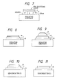
- Figs. 1 to 7 each show a typical model of a device of an MIS structure
- Figs. 8 to 10 each show that of an MIM structure
- Figs. 11 to 13 show each that of an IM structure.
- the polymer compound to be used in the present invention may be selected from among those which are described in JP-A-63-218728, and 63-3024 .
- it may be a polymer compound having linear repeating units wherein the first organic group R1 having at least two carbon atoms and at least 2 valences and the second organic group R2 having at least two carbon atoms and at least 2 valences are alternately bound to each other via a divalent binding group and at least one, preferably two, hydrocarbon-containing groups R3 having 10 to 30 carbon atoms and optionally containing substituent(s) is bound to said repeating unit via a covalent bond so as to make the compound hydrophobic.
- the hydrophobic nature may be imparted to the polymer compound by an ionic bond.
- a polymer compound to which a hydrophobic nature is imparted by an ionic bond has a repeating unit wherein the first organic group R1 having at least two carbon atoms and at least 3 valences and the second organic group R2 having at least two carbon atoms and at least 2 valences are alternately bound via a divalent binding group, and at least one hydrocarbon-containing group R3 having 10 to 30 carbon atoms and optionally substituent(s) is bound to said repeating unit via an ionic bond.
- the polymer compound has a precursor structure capable of forming a five- or six-membered ring. This is because such a structure can be converted into a five- or six-membered ring structure excellent in heat resistance.
- Preferred examples of the polymer compound to which a hydrophobic group has been introduced via a covalent bond are as follows. wherein R6 represents a R7 represents an alkyl or an aryl group;
- R3 represents a hydrocarbon-containing group having 10 to 30, preferably 16 to 22 carbon atoms.
- a preferred example thereof is a monovalent group selected from aliphatic groups, those wherein an alicyclic group is bound to an aliphatic one and those wherein an aromatic group is bound to an aliphatic one, each optionally substituted. Examples thereof are as follows: wherein n is 10 to 30, preferably 16 to 22. Among these groups, a straight-chain aliphatic hydrocarbon group is particularly preferred.
- substituent R3 examples include halogen atoms, nitro, amino, cyano, methoxy and acetoxy groups. However it is sometimes preferred to use a fluorine atom which can elevate the hydrophobic nature of the polymer compound, compared with a hydrogen atom.
- the R3 alkyl chain can be shortened by introducing fluorine atom(s) thereto.
- k is 2, which enables the formation of a film with 10 carbon atoms.
- the molecular weight of the polymer compound to be used in the present invention is not particularly restricted. Although a film can be produced according to the process of the present invention by using a polymer compound having a low molecular weight, however, the resulting film is poor in heat resistance, mechanical strength and chemical resistance. On the other hand, an excessively high molecular weight of the polymer compound brings about such a high viscosity as to make the film-formation difficult.
- the number-average molecular weight of the polymer compound may range from about 2,000 to 300,000, preferably from about 10,000 to 150,000.
- the present invention involves a case wherein either the compound of (3-1) or (3-2) is present alone as well as that wherein both of the compounds of (3-1) and (3-2) are present together.
- at least one of R3, R4 and R5 is the same as the R3 defined in the formulae (1) to (20) and examples thereof, while the other groups each represent an optionally substituted hydrocarbon-containing group having 1 to 30 carbon atoms or a hydrogen atom.
- a hydrocarbon-containing group having 1 to 4 carbon atoms and a hydrogen atom are preferred.
- a mixture of these polymer compounds are also available in the present invention.
- the process for forming LB film comprises spreading a film-forming material on the surface of water, compressing the material thus spreaded on the surface of water at a constant surface pressure to form a monomolecular film, and then transferring the film formed onto a subtrate by repeatedly passing the substrate through the film.
- the vertical dipping method there may be mentioned horizontal dipping method, revolving cylindrical method, etc.
- Shin Jikken Kagaku Koza "vol. 18, “Interface and Colloid", 498-508). Any procedure may be employed without restriction, as long as it has been commonly employed in the art.
- the LB technique enables the production of an orientated film whose thickness is controlled with an accuracy of several tens ⁇ .
- it is an excellent method for producing a film of a thickness less than 200 ⁇ , less than 1000 ⁇ , several hundreds ⁇ , or several tens ⁇ .
- the film on the substrate of the present invention also has the above-mentioned characteristics. However, a film of thickness 10,000 ⁇ or more, may be produced thereby.
- a compound represented by the formula CH3(CH2) n-1 Z is preferred from the viewpoints of performance and cost.
- those containing unsaturated bond(s) can be polymerized by, for example, UV-irradiation.
- the ratio between at least one of these compounds and the polymer compound is not particularly specified.
- organic polar solvent examples include N,N-dimethylformamide, N,N-dimethylacetamide, N,N-diethylformamide, N,N-diethylacetamide, N,N-dimethylmethoxyacetamide, dimethylsulfoxide, N-methyl-2-pyrrolidone, pyridine, dimethylsulfone, hexamethylphosphoramide, tetramethylenesulfone and dimethyltetramethylenesulfone.
- the substrate to be used in the present invention is not considerably restricted by anything other than the purpose of the application of the obtained film.
- commonly employed inorganic substrates made of, for example, glass, alumina or silica as well as those containing semiconductors of IV, III-V and II-VI groups such as metals, Si, GaAs and ZnS, ferroelectric materials such as PbTiO3, BaTiO3, LiNbO3 and LiTaO3 and magnetic thin films may be employed therefor.
- a surface-treated substrate may be preferably used in the embodiment of the present invention.
- a LB film, built-up on a substrate, is irradiated with an excimer laser through a mask, if desired.
- Preferred examples of the excimer laser are KrF, ArF and XeCl types.
- the film is irradiated with the excimer laser having a high energy density, the irradiated part is removed, which makes it possible to produce a patterned thin film without requiring any development step by using a developing solution.
- an organic solvent such as methanol or ethanol, aqueous ammonia, or an organic or inorganic alkaline solution may be used as a developing solution in the present invention.
- the pulse energy of the excimer laser is at least 5 mJ/cm2, more preferably at least 10 mJ/cm2, though it varies depending on the pulse interval.
- the polymer compound of the present invention having the pattern thus obtained can be converted into a five- or six-membered ring structure to give a heat resistant polymer film pattern, when said polymer compound has a precursor structure capable of giving a five- or six-membered ring structure.
- a precursor structure capable of giving a five- or six-membered ring structure is formed from a precursor structure capable of giving a five- or six-membered ring structure.
- those of the formulae (3) to (15) and (21) to (30) are capable of partial or complete ring closure so as to give a five- or six-membered ring involving hetero atom(s).
- each compound has the following strucutre:
- the method for the ring closure is not particularly restricted.
- the compound of the formula (5) may be imidized to give an imide of the formula (5′) through ring closure by heating to 300 to 400 °C, as shown below.
- a group which has been introduced in order to make the polymer compound hydrophobic is liberated as an alcohol.
- This alcohol can be vaporized at a temperature of 200 to 400 °C under a gas stream or under reduced pressure, if required.
- a polyimide film having excellent heat resistance can be obtained.
- a chemical curing agent such as acetic anhydride, pyridine or isoquinoline commonly employed in the imidization of a compound may be used optionally upon heating.
- the film which has been produced by building-up the polymer compound of the present invention on a substrate by the Langmuir-Blodgett technique, patterning the built-up film thus obtained and optionally subjecting the same to ring closure is excellent in heat resistance, mechanical properties and chemical resistance, and has high electric insulating characteristics. Furthermore, this film is extremely thin, namely, 10000 ⁇ or below in thickness. The thickness thereof may be lowered to 5000 ⁇ , 2000 ⁇ or even 10 to 1000 ⁇ , if desired.
- this film sustains excellent physical properties, in particular, a breakdown strength of 1 x 10⁶ V/cm or more, even at a thickness less than 1000 ⁇ , for example, several hundreds ⁇ or 50 to 100 ⁇ , which makes it useful in various devices. It is expected, in particular,that a film having a thickness of 50 to a few hundreds ⁇ would exert a specific effect such as a tunnel effect, which can be applied to various interesting purposes.
- the patterned thin film of the present invention is excellent in heat resistance, chemical resistance and mechanical properties and has an extremely low thickness, which makes it widely available in the fields of, for example, electronics, energy conversion and separation of materials.
- the chemical resistance of this film makes it useful as a photoresist in the field of microprocessing of semiconductors.
- the patterned thin film of the present invention is extremely thin, which makes it available as a resist for microprocessing at a submicronic or quartermicronic level. Furthermore, the excellent heat resistance of the patterned thin film of the present invention makes it applicable to a dry etching process.
- Typical examples of a dry etching process include plasma etching, reactive sputter etching and reactive ion beam etching. Namely, various materials such as Si, polysilicon, SiO2, Si3N4 or Al may be processed by these methods by appropriately selecting a reactive gas from, for example, CF4, CF4 + O2, CF4 + H2, C3H8, CCl4 and BCl3.
- the patterned thin film of the present invention which is excellent in photoconductivity, optical properties, insulating characteristics, thermal properties and chemical reactivity, may be applied as such to an electrical/electronic device in the field of electronics.
- the primary important electrical/electronic device involving the thin film of the present invention is a metal/insulator/semiconductor device, which will be called a MIS device hereinafter. It is a basic structure for the construction of a planar electronic device or an integrated circuit.
- Figs. 1 to 7 each show a typical model of the above-mentioned MIS device.
- the thin film of the present invention is formed on a semiconducting substrate and a metal electrode is placed thereon.
- the semiconductor may be selected from those of the IV group of the Periodic Table such as Si or Ge, those of the III-V group such as GaAs or GaP and those of the II-VI group such as CdTe, CdS, ZnS, ZnSe or CdHgTe.
- various transducers e.g.
- photoelectric conversion elements such as solar cells, light emitting elements such as LED (light emitting diode), EL (electroluminescence) or photodiods, light receiving elements, light detecting elements, gas sensors, or temperature sensor.
- the semiconductor to be used in the present invention may be either monocrystalline, polycrystalline or amorphous.
- Fig. 2 The model of Fig. 2 is the same as that of Fig. 1 except that two or more devices are formed on a single substrate. It is an interesting example of the application of the present invention whereby a charge-transfer device such as charge-coupled device (CCD) can be obtained.
- CCD charge-coupled device
- a semiconductor which is frequently provided in the form of a semiconducting film is formed on an insulating substrate provided with an electrode, which may be either transparent or patterned, and the thin film of the present invention is formed thereon.
- the model of Fig. 4 differs from that of Fig. 3 in that a thin film is inserted between an electrode in the side of an insulating substrate and a semiconducting film.
- the semiconducting film may be produced by any method commonly employed in the art, for example, molecular beam epitaxy (MBE), metal organic chemical vapour deposition (MOCVD), atomic layer epitaxy (ALE), vacuum evaporation, sputtering, spray pyrolysis or coating.
- the semiconductor may be selected from those cited above regarding Figs. 1 and 2. Thus, devices similar to those described in these cases may be obtained.
- a semiconducting film is formed on the thin film of the present invention. It is undesirable that the heat of formation of the semiconducting film exceeds the tolerance limit of the heat resistance of the thin film of the present invention. However, a film obtained through ring-closure can sufficiently withstand the building-up of, for example, amorphous silicon. Furthermore, recent developments in the low temperature formation techniques for semiconductors will make this process applicable to a number of semiconductors.
- FIGs. 5 and 6 are schematic models showing typical embodiments of an MIS devices having a field effect transistor (FET) structure (hereinafter referred to as "MISFET device”), which are drived by controlling the channel current with gate electrodes and which are the most important device among MIS devices.
- FET field effect transistor
- a semiconducting substrate is used.
- a semiconductor which is frequently provided in the form of a semiconducting film is formed on a insulating substrate in that of Fig. 6.
- the MISFET is a basic type of device and is applicable to various devices.
- a thin film transistor for driving a liquid crystal display may be formed by constructing this sturcture on a substrate of a large area.
- an integrated circuit may be formed by elevating the degree of integration of the same.
- an insulating film is incorporated thereto, optionally together with a film, sensitive to, for example, an ion, a gas or an active substance, an ion-sensitive FET (ISFET), a gas-sensitive FET (ChemFET), an immunological FET (IMFET) or an enzyme FET (ENFET) can be obtained.
- ISFET ion-sensitive FET
- ChemFET gas-sensitive FET
- IFET immunological FET
- ENFET enzyme FET
- each FET can be explained by the field effect that appears when an ion, a gas or an active substance comes into contact with the surface of the gate insulating film.
- the use of the thin film of the present invention makes further modifications of the same with various organic materials advantageous, compared to a case where conventional inorganic material is employed. It is particularly advantageous to utilize the interaction between hydrophobic long-chain alkyl group(s) in the film, if any, and a hydrophobic portion of a protein.
- a semiconducting film is formed on a quartz substrate and an insulating film and an ion-sensitive film are further located thereon.
- the thin film of the present invention is available as said insulating film.
- a compound semiconductor which can hardly be formulated into an excellent insulating film by a conventional manner such as oxidation for example, those belonging to the groups of III-V and II-VI, is to be used as a semiconductor in the construction of a device of the MIS structure.
- GaAs is used in practice as a metal-semiconductor FET (MESFET). It is expected that the use of the same as the MIS structure would further improve the performance of the obtained device.
- GaAs to the construction of a MIS integrated circuit is advantageous not only in that the driving voltage can be lowered thereby, but also in that an integrated circuit capable of working at a high speed can be readily produced by taking advantage of the large carrier mobility in the GaAs semiconductor.
- the second important electrical/electronic device comprising the thin film of the present invention is a metal/insulator/metal device, which will be called a MIM device.
- Figs. 8 to 10 each show a model of the MIM device wherein a metal, an insulating film and another metal is formed in this order on an insulating substrate or a semiconducting substrate.
- Fig. 8 shows the structure of a capacitor.
- the change in the capacitance caused by moisture is monitored, it may serve as a moisture sensor.
- a transistor of the MIM structure may be formed by using the same.
- the structure shown in Fig. 9 enables the construction of a hot electron transistor.
- a capacitor for a memory cell of a VLSI may be obtained by forming a capacitor on a semiconductor or a semiconducting device.
- Fig. 10 may be applied to a device wherein a hot electron is introduced into a semiconductor.
- a Josephson junction (JJ) device may be produced by substituting the metal with a superconductor such as Nb.
- the third electrical/electronic device comprising the thin film of the present invention is an insulating film/metal (IM) device.
- Fig. 11 shows a typical model of the most simple type thereof the thin film of the present invention is formed as an insulating film on a metal.
- An example of the application of this device is a liquid crystal orientation film obtained by forming the thin film of the present invention on a patterned electrode which is usually a transparent electrode such as ITO.
- Figs. 12 and 13 show additional examples of the application of the above-mentioned device.
- the thin film of the present invention is formed between two electrodes independently from each other.
- the device thus formed is available as, for example, a sensor for moisture or a gas.
- the refractive index of the thin film of the present invention may be adjusted by precisely controlling the thickness and selecting an appropriate compound which makes it highly useful as a component of an optical circuit.
- a mixed or laminated film comprising a functional LB material and a fatty acid
- said fatty acid may be substituted by the polymer of the present invention, whereby various functions may be imparted to the film thus obtained. Therefore the film thus produced is widely applicable to various purposes. For example, a film which contains a colorant or an enzyme and thus available in a photoelectrical transducer or a biosensor may be obtained thereby.
- a patterned thin film can be produced without requiring any developing procedure by irradiating a polymer LB film with an excimer laser having a high energy density.
- a patterned thin film which is excellent in heat resistance and has good chemical resistance and mechanical properties in addition to a low thickness as not usually achieved in a conventional manner, namely, 10000 ⁇ or below or 10 to 1000 ⁇ , if required, can be produced by partially or completely cyclizing said polymer and simultaneously vaporizing a known LB film compound mixed therewith.
- reaction product thus obtained was dissolved in 40 ml of hexamethylphosphoric triamide and cooled to 0 to 5 °C. Next, 2.38 g of thionyl chloride was added dropwise thereto at approximately 5 °C. After the completion of the addition, the resulting mixture was maintained at approximately 5 °C for an hour to thereby complete the reaction.
- the powder thus obtained was subjected to IR spectrometry, thermogravimetric analysis (TGA-DTA) and molecular weight- determination by GPC.
- a mixture of the obtained powder and stearyl alcohol at a molar ratio of 1 : 1 was dissolved in a mixture of distilled chloroform and dimethylacetamide (8 : 2 by volume) to thereby give 25 ml of a solution for the spreading of an LB film.
- a monomolecular film was prepared by spreading the solution obtained above on the surface of redistilled water at 20 °C. Then the obtained film was vertically built-up on a silicon semiconducting substrate while maintaining the surface pressure at 2.5 Pa (25 dyne/cm) a building-up rate of 10 mm/min to thereby form 31 layers.
- the built-up film thus obtained was irradiated with 10 pulses of an ArF excimer laser of a pulse energy of 50 mJ/cm2 through a test mask. As a result, the irradiated part of the built-up film was removed and thus a positive pattern (0.4 ⁇ m) was formed.
- the sensitivity was as high as 500 mJ/cm2.
- the patterned built-up film was further heated to 400 °C for an hour. It was proved from peaks at 1790 cm ⁇ 1 and 1710 cm ⁇ 1 in FT-ATR-IR analysis that an ⁇ , ⁇ -unsaturated five-membered ring imide ring was formed thereby.
- silicon was etched with a gas mixture (CF4 + O2) by using the above-mentioned resist pattern as a mask.
- CF4 + O2 a gas mixture
- Talystep method it was found by Talystep method that a difference in the level at a depth of 2 ⁇ m was formed in the silicon.
- a similar result was obtained by irradiating the film with 25 pulses of an ArF excimer laser of a pulse energy of 25 mJ/cm2.
- a similar result was obtained by irradiating the same with 70 pulses of an ArF excimer laser of a pulse energy of 10 mJ/cm2.
Landscapes
- Physics & Mathematics (AREA)
- Spectroscopy & Molecular Physics (AREA)
- General Physics & Mathematics (AREA)
- Application Of Or Painting With Fluid Materials (AREA)
Applications Claiming Priority (4)
| Application Number | Priority Date | Filing Date | Title |
|---|---|---|---|
| JP20974988A JPH0259069A (ja) | 1988-08-24 | 1988-08-24 | パターン化された超薄膜の製法 |
| JP209749/88 | 1988-08-24 | ||
| JP5267689A JPH02232265A (ja) | 1989-03-03 | 1989-03-03 | パターン化された超薄膜の製法 |
| JP52676/89 | 1989-03-03 |
Publications (2)
| Publication Number | Publication Date |
|---|---|
| EP0355810A2 true EP0355810A2 (fr) | 1990-02-28 |
| EP0355810A3 EP0355810A3 (fr) | 1990-09-05 |
Family
ID=26393313
Family Applications (1)
| Application Number | Title | Priority Date | Filing Date |
|---|---|---|---|
| EP19890115561 Withdrawn EP0355810A3 (fr) | 1988-08-24 | 1989-08-23 | Procédé de structuration de films minces |
Country Status (1)
| Country | Link |
|---|---|
| EP (1) | EP0355810A3 (fr) |
Cited By (1)
| Publication number | Priority date | Publication date | Assignee | Title |
|---|---|---|---|---|
| US8377544B2 (en) | 1999-07-29 | 2013-02-19 | Mitsubishi Gas Chemical Company, Inc. | Glass fabric base material/thermosetting resin copper-clad laminate having a high-elasticity |
Family Cites Families (3)
| Publication number | Priority date | Publication date | Assignee | Title |
|---|---|---|---|---|
| US4693958A (en) * | 1985-01-28 | 1987-09-15 | Lehigh University | Lithographic plates and production process therefor |
| JPS633024A (ja) * | 1986-06-20 | 1988-01-08 | Kanegafuchi Chem Ind Co Ltd | イオン結合を含む高分子化合物 |
| EP0262446B1 (fr) * | 1986-09-04 | 1993-07-21 | Kanegafuchi Kagaku Kogyo Kabushiki Kaisha | Polymères amphiphiles photosensibles à haut poids moléculaire et leur procédé de production |
-
1989
- 1989-08-23 EP EP19890115561 patent/EP0355810A3/fr not_active Withdrawn
Cited By (1)
| Publication number | Priority date | Publication date | Assignee | Title |
|---|---|---|---|---|
| US8377544B2 (en) | 1999-07-29 | 2013-02-19 | Mitsubishi Gas Chemical Company, Inc. | Glass fabric base material/thermosetting resin copper-clad laminate having a high-elasticity |
Also Published As
| Publication number | Publication date |
|---|---|
| EP0355810A3 (fr) | 1990-09-05 |
Similar Documents
| Publication | Publication Date | Title |
|---|---|---|
| EP0246602B1 (fr) | Dispositif comportant une couche mince en polymère | |
| US4943471A (en) | Patterned thin film and process for preparing the same | |
| EP0237017B1 (fr) | Dispositif du type électrique ou électronique comportant une couche mince de polyimide | |
| JPS62129316A (ja) | ポリイミド前駆体を部分的に閉環させた薄膜 | |
| US4910293A (en) | Langmuir-Blodgett films of polymers having pendent C10 -C30 hydrocarbon groups | |
| US20080315192A1 (en) | Integrated Circuit Comprising an Organic Semiconductor, and Method for the Production of an Integrated Circuit | |
| EP0218114B1 (fr) | Film et son procédé de fabrication | |
| JPH0626704B2 (ja) | 基板との接着性が改良された超薄膜とその製法 | |
| EP0403817B1 (fr) | Structures diélectriques comprenant du matériau résistant au décapage et son procédé de fabrication | |
| EP0247358A2 (fr) | Précurseur de copolymère polyimide amphiphile, son procédé de préparation et film fin | |
| CA1303281C (fr) | Couche mince a motif alterne, procede de fabrication | |
| US4868281A (en) | Ionic bond containing condensation polymers | |
| US20080139766A1 (en) | Perfluoroalkyleneoxy group-substituted phenylethylsilane compound and polymer thereof | |
| JPH0259069A (ja) | パターン化された超薄膜の製法 | |
| JPH02232265A (ja) | パターン化された超薄膜の製法 | |
| EP0239980A2 (fr) | Dispositif électrique-électronique incluant une couche mince en polyimide | |
| US4988570A (en) | Process for forming a film | |
| JPH0749110B2 (ja) | ポリイミド前駆体薄膜を含む複合物品 | |
| JPS63126578A (ja) | 薄膜を含む複合物品 | |
| JPH0236237A (ja) | パターン化された簿膜およびその製法 | |
| JP5458296B2 (ja) | 微細加工構造及びその加工方法並びに電子デバイス及びその製造方法 | |
| JPH0671575B2 (ja) | 薄 膜 | |
| JPH058094B2 (fr) | ||
| Kabeta et al. | Photochemical conversion of electrically conductive polysilane films into insulators | |
| JPH01232037A (ja) | 感光性両性高分子化合物の薄膜を含む複合物品 |
Legal Events
| Date | Code | Title | Description |
|---|---|---|---|
| PUAI | Public reference made under article 153(3) epc to a published international application that has entered the european phase |
Free format text: ORIGINAL CODE: 0009012 |
|
| AK | Designated contracting states |
Kind code of ref document: A2 Designated state(s): BE DE FR GB |
|
| PUAL | Search report despatched |
Free format text: ORIGINAL CODE: 0009013 |
|
| AK | Designated contracting states |
Kind code of ref document: A3 Designated state(s): BE DE FR GB |
|
| 17P | Request for examination filed |
Effective date: 19901228 |
|
| STAA | Information on the status of an ep patent application or granted ep patent |
Free format text: STATUS: THE APPLICATION HAS BEEN WITHDRAWN |
|
| 18W | Application withdrawn |
Withdrawal date: 19930113 |