EP0357278A2 - Vielseitiges Steuersystem, das eine Mikrosteuerung verwendet - Google Patents
Vielseitiges Steuersystem, das eine Mikrosteuerung verwendet Download PDFInfo
- Publication number
- EP0357278A2 EP0357278A2 EP89308211A EP89308211A EP0357278A2 EP 0357278 A2 EP0357278 A2 EP 0357278A2 EP 89308211 A EP89308211 A EP 89308211A EP 89308211 A EP89308211 A EP 89308211A EP 0357278 A2 EP0357278 A2 EP 0357278A2
- Authority
- EP
- European Patent Office
- Prior art keywords
- microcontroller
- address
- bus
- eeprom
- addresses
- Prior art date
- Legal status (The legal status is an assumption and is not a legal conclusion. Google has not performed a legal analysis and makes no representation as to the accuracy of the status listed.)
- Withdrawn
Links
Images



Classifications
-
- G—PHYSICS
- G06—COMPUTING OR CALCULATING; COUNTING
- G06F—ELECTRIC DIGITAL DATA PROCESSING
- G06F9/00—Arrangements for program control, e.g. control units
- G06F9/06—Arrangements for program control, e.g. control units using stored programs, i.e. using an internal store of processing equipment to receive or retain programs
- G06F9/22—Microcontrol or microprogram arrangements
-
- G—PHYSICS
- G05—CONTROLLING; REGULATING
- G05B—CONTROL OR REGULATING SYSTEMS IN GENERAL; FUNCTIONAL ELEMENTS OF SUCH SYSTEMS; MONITORING OR TESTING ARRANGEMENTS FOR SUCH SYSTEMS OR ELEMENTS
- G05B19/00—Program-control systems
- G05B19/02—Program-control systems electric
- G05B19/04—Program control other than numerical control, i.e. in sequence controllers or logic controllers
- G05B19/042—Program control other than numerical control, i.e. in sequence controllers or logic controllers using digital processors
Definitions
- the invention relates to electronic control systems that utilize a microcontroller, (a limited-capability central processing unit contained on one semiconductor chip.) Electronic control systems that are based on microcontrollers and that utilize external memories and/or auxiliary "slave" microcontrollers often require the support of a number of ancillary circuits to perform functions related to the system bus. This invention includes an ancillary integrated circuit capable of performing these functions in a wide variety of applications of electronic control systems.
- AMT automated mechanical transmission
- actuators such as pneumatic or electromechanical actuators.
- the invention is a versatile multipurpose electronic control apparatus utilizing certain types of microcontrollers.
- One object of the invention is to provide tri-statable address latches for enabling an external programmer to program Erasable Programmable Read-Only Memories (EPROMs) of the system that are external to a Main Microcontroller.
- EPROMs Erasable Programmable Read-Only Memories
- Another object is to provide a very flexible Address Decoder that is capable of accommodating a great variety of memory maps.
- Another object is to provide flexible write Protection for Electrically Erasable Programmable Read-Only Memories (EEPROMs).
- EEPROMs Electrically Erasable Programmable Read-Only Memories
- the write protection reduces the risk that information in memory will be inadvertently erased by writing over it; differing compromises between protection and convenience are provided within a single EEPROM.
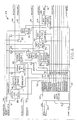
- An electronic control unit for controlling an AMT is the preferred example of use of the invention. It is designated generally in FIGS. 1 and 2 by reference numeral 2.
- the disclosures of the following United b States Patents, which provide detailed information about the AMT environment, are incorporated herein by reference: No. 4,361,060; No. 4,551,802; No. 4,567,263; No. 4,702,127.
- the electronic control unit 2 of the particular AMT embodiment being described utilizes a Main Microcontroller 4. model no. 8097BH, manufactured by Intel Corporation, of 3065 Bowers Avenue, Santa Clara, CA, 95051 (or similar microcontrollers). It has an external bus 6 for connection to additional memory such as external EPROM 8, RAM 12, and EEPROM 16, (with adjustable bus width), and for other I/O functions, including connection of a slave microcontroller 18 if desired.
- a Main Microcontroller 4 model no. 8097BH, manufactured by Intel Corporation, of 3065 Bowers Avenue, Santa Clara, CA, 95051 (or similar microcontrollers). It has an external bus 6 for connection to additional memory such as external EPROM 8, RAM 12, and EEPROM 16, (with adjustable bus width), and for other I/O functions, including connection of a slave microcontroller 18 if desired.
- the invention includes an Ancillary Circuit 20 on a single chip that performs bus-related functions in a wide variety of applications. Because of its versatility, the invented electronic control system is usable also as a standard building block for many applications other than control of an AMT.
- the Ancillary Circuit 20 eliminates various "glue" chips that are usually required for assembling a system and provides a simple means of attaching an optional slave microcontroller such as block 18.
- FIGS. 1 and 2 illustrate how this device 20 would be connected into a system having a slave microcontroller.
- the Ancillary Circuit 20 has four functional blocks (FIG. 3), namely: o Address Latches 22 o Address Decoder 24 o EEPROM Write Inhibit Logic 26 o External Interface Circuit 28. These blocks are described separately below.
- the 8097BH microcontroller 4 has 16 time-multiplexed address and data lines for its system bus 6.
- the lines are used to transmit an address at the beginning of a bus cycle and data later in the same cycle.
- the multiplexing requires that latches 22 be provided to hold the addresses for the external memories 8, 12, 16, during the portion of each bus cycle in which the bus 6 is being used to transfer data, FIG. 3.
- EPROM 8 program memory
- the procedure requires that the address latches 22 be tri-statable so that the External Prom Programmer 30 can take control of the address bus 32.
- Address latches 22 of this invention therefore include output drivers 34 (FIG. 3) capable of outputting three states, one of which has a high impedance that permits control of the address bus 32 to be driven by an external device.
- the tri-statable drivers 34 are logic devices that are controlled by a PGMPROM signal at a terminal 36; their outputs are in the high impedance state when PGMPROM is high. When PGMPROM is low the drivers 34 function as amplifiers that transmit the outputs of the address latches 22 to the bus 32.
- the desired external characteristics of the drivers 34 can be achieved in any of many routine designs, for example, the PGMPROM signal can drive a series-connected semiconductor from conduction to cutoff.
- the tri-statable drivers 34 allow the EPROM 8 to be programmed without removing it from the circuit, so it is unnecessary to provide sockets for holding the EPROMs.
- the address latches 22 are of a transparent type by which the address is made available to the external devices 8, etc. even before it is actually locked in at the latches 22.
- the latches 22 are open to receive addresses when an Address Latch Enable (ALE) signal at terminal 38 is high, and closed when it is low.
- ALE Address Latch Enable
- Address Decoder 24 is flexible enough to accommodate a variety of memory maps.
- a memory map is a representation of the organization of memories, i.e., RAM, EPROM, EEPROM, I/O, within the address space of the processor.
- the 8097BH microcontroller 4 is designed to accommodate both 8-bit-wide and 16-bit-wide devices 8, etc., simultaneously. In order to mix 8-bit and 16-bit devices on the same bus it is necessary to specify the bus width of the device at each memory location, e.g., the EPROM, (FIG. 4).
- PROMSEL′ (40, which has a tri-statable output driver 50) RAMSEL′ (42) EEPSEL′ (44) AUXSEL′ (46) BUSWIDTH (48).
- register select lines generated within the Address Decoder 24 that are used internally for controlling access to registers contained on the Ancillary Circuit chip itself, FIGS. 4 and 6. These lines and their signals, which are discussed further in a section below entitled “Internal Register Select Lines", are named: WREGWR Width register write 52 PREGWR PROMsel register write 54 RREGWR RAMsel register write 56 EREGWR EEPROM register write 58 AREGWR AUX register write 60 FIFORD FIFO read 62 FIFOWR FIFO write 64 STATRD Status register read 66 CNFIGWR Configuration register write 68 PORTARD PORTA read 70 PORTAWR PORTA write 72 PORTBRD PORTB read 74 PORTAWR PORTB write 76
- the purpose of the externally accessible address select lines 40 etc. and the bus width signal at line 48 is to provide an ability to access memory configurations that are likely to be needed for various systems, without requiring additional small-scale and medium-scale integrated circuitry. Because this Ancillary Circuit is intended to be used in applications with as-yet-undefined memory maps, a capability has been provided for it to be dynamically configured in order to accommodate a variety of system requirements. This is done by providing internal registers 78, 80, 82, 84, in the Address Decoder 24 of the Ancillary Circuit 20, to receive and store the address information of bus 6, to which it responds by operating its four chip select lines 40, 42, 44, 46, respectively. See FIG. 4.
- Block 78 consists of eight D-type flip-flops with asynchronous clear (RESET). The flip-flops are clocked by the rising edge of the PREGWR signal.
- Each of the registers 78, etc. is connected with a Decode Logic circuit; e.g., Prom Register 78 is connected with Prom Decode Logic circuit 88.
- the Decode Logic circuit 88 recognizes it, and outputs a signal to its tri-statable driver (switch) 50, which, if not then preempted by a PGMPROM command 36, transmits the signal via the PROMSEL line 40 to the EPROM 8.
- PROMSEL /(A13 * /A14 * /A15 + /A13 * /A14 * A15 * PROMREG2 + /A13 * A14 * /A15 * PROMREG1 + /A13 * A14 * A15 * PROMREG4 + A13 * /A14 * A15 * PROMREG3 + A13 * A14 * /A15 * PROMREG2 + /A12 * A13 * A14 * A15 * PROMREG5 + A12 * /A13 * /A14 * /A15 * PROMREG0 + /A11 * A12 * A13 * A14 * A15 * PROMREG6 + /A04 * A11 * A12 * A13 * A14 * A15 * PROMREG7 + /A05 * A11 * A12 * A13 * A14 * A15 * PROMREG7 + /A06 * A11 * A12 *
- the driver 50 is similar to the drivers 34 which are described elsewhere herein. In the same way (except without line drivers such as driver 50), Registers 80, 82, and 84 are connected with RAM Decode, EEP Decode, and AUX Decode Logic circuits respectively, which provide output signals to the lines RAMSEL, EEPSEL, and AUXSEL respectively when one of those external devices is selected.
- the Width Register 86 receives address information on the bus 6 (FIG. 4), which is decoded in the Width Decode Logic circuit 96.
- the output of circuit 96 is the BUSWIDTH line 48. It is connected to an input terminal of the Main Microcontroller 4, as shown in FIGS. 1 and 2.
- the Width Register 86 can be programmed by means of a command on the WREGWR output line 52 of the Register Address Decoder 100.
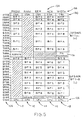
- the memory map 104 of FIG. 5 depicts on its vertical axis 106 various memory regions of the 8097BH Main Microcontroller 4, and on its horizontal axis 108 each of the Select lines.
- An example is the line PROMSEL′, 40. It is abbreviated in the heading of column 110 as PROM, and represents the EPROM, 8. Columns 112, 114, and 116 correspond to RAM, EEPROM, and AUX, respectively.
- the BUSWIDTH line 48 is represented on the map 104 by the last column 118.
- Each block within a column 110, 112, 114, 116 of the map represents a region within one of the external memories such as EPROM 8, to which a particular address from the Main Microcontroller 4 can be mapped.
- the register bit in the PROM register 78 that enables the mapping of each block is indicated in the block of column 110, and columns show similar bit numbers.
- PROMSEL′ This signal is used for selecting the program memory chips EPROM, 8.
- the 8097BH Main Microcontroller 4 uses address 2080H as its reset vector address and the addresses between 2000H and 200EH for its interrupt vectors. Therefore, it is necessary that it always be possible to access the EPROM at these locations regardless of the state of the configuration registers. Addresses between 2000H and 3FFFH always cause PROMSEL′ to be driven true (low state). Any other addresses to be selected with this signal must be specified via the associated 8-bit PROMSEL register 78.
- bits within this register are defined as follows: BIT ADDRESS RANGE 0 1000H - 1FFFH 1 4000H - 5FFFH 2 6000H - 9FFFH 3 A000H - BFFFH 4 C000H - DFFFH 5 E000H - EFFFH 6 F000H - F7FFH 7 F800H - FFEFH
- PROMON input signal on line 120 FIG. 4.
- PROMSEL′ signal, 40 When it is desired to run from an off-board memory, the PROMON signal 120 is pulled low, which causes the PROMSEL′ signal 40 to remain false (high state).
- the PROMSEL Register 78 is cleared to all zeros by driving the RESET′ line 122 true (low state).
- the registers RAM (80), EEP (82), AUX (84), and WIDTH (86) are cleared in the same way.
- PROMSEL′ signal 40 Since external prom programming requires the EPROM 8 to be selected by an External Prom Programmer 30, it is necessary for the PROMSEL′ signal 40 to be tri-statable.
- the PGMPROM signal at 36 is used to control the PROMSEL′ tri-statable driver 50, FIG. 4. When PGMPROM 36 is high PROMSEL′ 40 is switched to a high-impedance state.
- RAMSEL′ This signal line 42 is used for selecting the scratch pad and variable data memory chips of the RAM 12.
- the 8097BH contains 232 general-purpose registers located between addresses 18H - FFH.
- the spaces are denoted "CPU", in a row designated 124 of map 104. It is convenient for the user, therefore, for any additional random access memory to be placed directly above these registers in the system address space. Addresses between 0100H and 01FFH, column 112 of map 104, always cause the RAMSEL′ line to be driven true (low state). Any other addresses selected by this RAMSEL′ signal must be specified via the associated 8-bit RAMSEL Register 80.
- EEPSEL′ This signal is used for selecting Electrically Erasable Programmable Read Only Memory 16, which is the parameter storage memory (EEPROM).
- EEPROM Electrically Erasable Programmable Read Only Memory
- the EEPROM is selected by means of the EEPSEL′ line 44, FIG. 4.
- Bit 7 of the register 82 is a control bit that specifies the upper or lower half of the chip select map 104 of FIG. 5. When bit 7 is a logic 1, the other bits, zero to 6, are properly interpreted in accordance with the upper byte of the map. When bit 7 is a logic zero, those other bits are interpreted by the lower byte of the map.
- the address bus 32 is connected to the EEP Decode Logic 92, to transmit address information A00 - A15.
- the address A00 - A15 on bus 32 is the output of the address latches 22; it is the same address as was originally transmitted by the Main Microcontroller 4 on its system bus 6.
- the bus 32 also transmits the address data A00 - A15 directly to the EPROM 8, the RAM 12, and the EEPROM 16.
- the AUXSEL′ line 46 is an auxiliary chip select line provided to accommodate systems that require additional devices on the bus 6.
- Bit 7 of the register is a control bit that defines the interpretation of the remaining seven bits of the register, as was described above in relation to EEPROM′.
- the bus 32 transmits address information from the Address Latches 22 to the AUX Decode Logic 94, which also receives information from the AUX Register 84.
- the AUX Decode Logic 94 When a bit in the register 84 is set, the presence on bus 32 of one of the addresses associated (on the map 104) with that bit causes the AUXSEL′ line 46 to be driven true (low state).
- BUSWIDTH This signal, on line 48 (FIGS. 2, 3, and 4), is used to inform the 8097BH Main Microcontroller 4 of the bus width (8 or 16 bits) of the device (e.g., RAM 12) that is at the selected address.
- the Main Microcontroller 4 uses this information to determine which of the data lines of bus 6 will contain the requested data and how to sequence accesses to 16-bit information.
- the PWRWDTH pin 128, FIGS. 2, 3, and 4 defines the function of the BUSWIDTH pin 48 for this address range. If the PWRWDTH pin 128 is high, the BUSWIDTH pin 48 is high for these addresses; when the PWRWDTH pin is low, the BUSWIDTH pin is low for these addresses.
- the function of the BUSWIDTH Pin 48 for addresses in all other regions of column 118 of the map 104 is specified by the associated bits within the 16 bit BUSWIDTH register 86 (FIG. 4) as defined below.
- BIT ASSOCIATED ADDRESS RANGE 0 0100H - 01FFH 1 0200H - 03FFH 2 0400H - 05FFH 3 0600H - 07FFH 4 0800H - 09FFH 5 0A00H - 0BFFH 6 0C00H - 0DFFH 7 0E00H - 0FFFH 8 1000H - 1FFFH 9 4000H - 5FFFH A 6000H - 9FFFH B A000H - BFFFH C C000H - DFFFH D E000H - EFFFH E F000H - F7FFH F F800H - FFEFH
- the WIDTH Decode 96 receives inputs from the Width Register 86, the PWRWDTH line 128, and the latched address bus 32, as shown on FIG. 4. When a bit in the Width Register 86 is set, the presence on bus 32 of one lb of the addresses associated with that bit causes the BUSWIDTH line 48 to be driven high by the WIDTH Decode Logic 96, indicating that a 16-bit-wide device is at that address.
- the BUSWIDTH Register itself (86) is at address FFF4H. Because it is a 16-bit register, the BUSWIDTH signal at 48 responds high at that address. All other internal registers are 8 bits wide.
- the architecture of the Ancillary Circuit 20 requires that many of its internal registers be accessible by the 8097BH Main Microcontroller 4.
- the Address Decoder 24 of FIG. 4 contains the logic necessary to select each of these registers for read or write access as appropriate.
- a Register Address Decoder, block 100 performs the function. It is shown in more detail in FIG. 6.
- one input to the Register Address Decoder 100 is the WRL′ line 132. It carries a write low byte control signal from the Main Microcontroller 4.
- a PREG Write Logic block 134 receives this signal; it controls the write-only PROMSEL Register 78 of FIG. 4.
- the PREG Write Logic also receives inputs from the latched address bus 32. If a WRL′ signal occurs when the latched address bus 32 has the address FFF0H, the PREG Write Logic 134 outputs a PREGWR signal, which is conducted on line 54 to the PROMSEL Register 78.
- Other write-only logic circuits of the Register Address Decoder operate similarly.
- Block 136 SCONF Select Logic
- FFF8H When it receives its own address, FFF8H, it outputs a signal on line 138 to two NOR gates 140, 142.
- the gate 140 has another input from WRL′ line 132. Simultaneous occurrence of address FFF8H and a write signal WRL′ cause NOR gate 140 to output a Configuration Write signal CNFIGWR on line 68 to the write-only Configuration Register (not shown).
- NOR gate 142 receives a RD′ read control signal on a line 150 from the Main Microcontroller 4. When that signal coincides with address FFF8H from bus 32, the NOR gate 142 outputs a STATRD signal on a line 66 to a read-only FIFO Status Register (not shown).
- An Electrically Erasable Programmable Read-Only Memory (EEPROM) in a control system offers the convenience of a non-volatile memory that can easily be modified by the operational software. However, because it can be modified so easily, a greater risk exists for the data in it to be corrupted by noise or by an errant microcontroller, which can be affected by electromagnetic interference or low system voltage.
- EEPROM Electrically Erasable Programmable Read-Only Memory
- the first type is of application- specific parameters related to the configuration or values of the system being controlled, for example calibrations related to the wheel base of the truck, the engine, the number of gears in the transmission, etc. They may have to be entered only once or twice in the life of a system, for example when the system is tested before installation, and again later when it is installed in a particular truck.
- the other type of information may have to be updated relatively frequently (e.g., once or more per day).
- the invented system includes circuits that provide secure protection where required for the parametric information, at the same time that it is amenable to easy modification of data that must be up-dated more frequently.
- the problem is solved by controlling the output enable of the EEPROM 16 via an EEPOUT′ signal, line 146, FIG. 3.
- EEPROMs are ordinarily designed so that it is impossible to write to them if their output enable is true. Therefore, if a mechanism is provided whereby the output enable is always pulled true when the EEPSEL′ signal (the EEPROM select signal) is true for locations where it is known that writes should not be performed, a significant layer of protection has been added.
- the logic signal on pin 148 can be changed by means of an external jumper wire. If EEPLOCK 148 is false (grounded), then when such an access is made, EEPOUT′ 146 is pulled true only if the read line RD′ signal 150 is true (low state). Thus when the system is in the unprotected mode the output enable is on or off depending upon whether there is a read or write signal.
- EEPROM located from FE00H to FFEFH is not protected and can always be written by a valid write cycle.
- Convenient but unprotected storage (in the upper addresses) is provided for data that must be modified frequently, and strong hardware protection is available in the lower addresses for infrequently modified data.
- the state of the EEPLOCK pin 148 is readable by the Main Microcontroller via a status register.
- EEPOUT /(/A15 * EEPLOCK * /EEPSEL + /A14 * EEPLOCK * /EEPSEL + /A13 * EEPLOCK * /EEPSEL + /A12 * EEPLOCK * /EEPSEL + /A11 * EEPLOCK * /EEPSEL + /A10 * EEPLOCK * /EEPSEL + /A09 * EEPLOCK * /EEPSEL + /EEPSEL * /RD)
- the 8097BH was designed principally to be a stand-alone microcontroller; consequently, it does not have control signals that would enable it to be integrated easily into systems requiring more than one microcontroller. Significant overhead would be incurred in accomplishing the necessary intercontroller communications with a slave, for example for synchronization.
- the invented device provides a pair of First-In-First-Out (FIFO) memories to obviate the synchronization arrangements that are usually required when two microcontrollers communicate with each other.
- FIFO First-In-First-Out
- Each of these memories is one byte wide by 32 bytes deep. They are located in the External Interface 28, of FIG. 3.
- the other can be written by the slave 18 and read by the Main Microcontroller 4.
- FIFO memories have flexible interrupt capabilities so that either microcontroller can be interrupted by a variety of conditions occurring within the two FIFOs.
- Port A and Port B Two 8-bit ports that can be used independently as either input or output ports, are included on the Ancillary Circuit. They are called Port A and Port B. Twelve of the pins constituting each of these ports are multiplexed with an intercontroller communication interface (part of block 28, FIG. 3) between the slave microcontroller 18 and Main Microcontroller 4. The remaining four pins are always available for I/O activities.
Landscapes
- Engineering & Computer Science (AREA)
- Physics & Mathematics (AREA)
- General Physics & Mathematics (AREA)
- Software Systems (AREA)
- Theoretical Computer Science (AREA)
- Automation & Control Theory (AREA)
- General Engineering & Computer Science (AREA)
- Storage Device Security (AREA)
- Control Of Transmission Device (AREA)
- Stored Programmes (AREA)
- Read Only Memory (AREA)
- Microcomputers (AREA)
Applications Claiming Priority (2)
| Application Number | Priority Date | Filing Date | Title |
|---|---|---|---|
| US23736488A | 1988-08-29 | 1988-08-29 | |
| US237364 | 1988-08-29 |
Publications (1)
| Publication Number | Publication Date |
|---|---|
| EP0357278A2 true EP0357278A2 (de) | 1990-03-07 |
Family
ID=22893416
Family Applications (1)
| Application Number | Title | Priority Date | Filing Date |
|---|---|---|---|
| EP89308211A Withdrawn EP0357278A2 (de) | 1988-08-29 | 1989-08-14 | Vielseitiges Steuersystem, das eine Mikrosteuerung verwendet |
Country Status (6)
| Country | Link |
|---|---|
| EP (1) | EP0357278A2 (de) |
| JP (1) | JPH0367345A (de) |
| KR (1) | KR940002477B1 (de) |
| CN (1) | CN1042433A (de) |
| AU (1) | AU4021889A (de) |
| BR (1) | BR8904414A (de) |
Cited By (2)
| Publication number | Priority date | Publication date | Assignee | Title |
|---|---|---|---|---|
| RU2248606C1 (ru) * | 2003-05-27 | 2005-03-20 | Российская Федерация в лице Министерства Российской Федерации по атомной энергии - Минатом РФ | Устройство контроля однокристального микроконтроллера |
| KR100757720B1 (ko) * | 1999-10-27 | 2007-09-11 | 스미또모 가가꾸 가부시끼가이샤 | 진공 자외선 여기 물질용 형광체 |
Families Citing this family (5)
| Publication number | Priority date | Publication date | Assignee | Title |
|---|---|---|---|---|
| WO2002037288A2 (en) * | 2000-10-31 | 2002-05-10 | Koninklijke Philips Electronics N.V. | Extension for the advanced microcontroller bus architecture (amba) |
| US7036054B2 (en) * | 2003-07-02 | 2006-04-25 | Nokia Corporation | Memory bus checking procedure |
| CN103616836A (zh) * | 2013-11-28 | 2014-03-05 | 盛瑞传动股份有限公司 | 一种自动变速器用存储芯片 |
| CN104500717A (zh) * | 2014-09-04 | 2015-04-08 | 厦门大学 | 一种工程车辆换挡控制装置 |
| CN110022101B (zh) * | 2019-04-04 | 2024-04-19 | 苏州国科视清医疗科技有限公司 | 基于fsmc的多步进电机驱动方法、电路及装置 |
-
1989
- 1989-08-14 EP EP89308211A patent/EP0357278A2/de not_active Withdrawn
- 1989-08-25 AU AU40218/89A patent/AU4021889A/en not_active Abandoned
- 1989-08-25 CN CN89106965A patent/CN1042433A/zh active Pending
- 1989-08-29 BR BR898904414A patent/BR8904414A/pt unknown
- 1989-08-29 KR KR1019890012349A patent/KR940002477B1/ko not_active Expired - Lifetime
- 1989-08-29 JP JP1222766A patent/JPH0367345A/ja active Pending
Cited By (2)
| Publication number | Priority date | Publication date | Assignee | Title |
|---|---|---|---|---|
| KR100757720B1 (ko) * | 1999-10-27 | 2007-09-11 | 스미또모 가가꾸 가부시끼가이샤 | 진공 자외선 여기 물질용 형광체 |
| RU2248606C1 (ru) * | 2003-05-27 | 2005-03-20 | Российская Федерация в лице Министерства Российской Федерации по атомной энергии - Минатом РФ | Устройство контроля однокристального микроконтроллера |
Also Published As
| Publication number | Publication date |
|---|---|
| BR8904414A (pt) | 1990-04-17 |
| KR940002477B1 (ko) | 1994-03-24 |
| JPH0367345A (ja) | 1991-03-22 |
| AU4021889A (en) | 1990-03-01 |
| KR900003742A (ko) | 1990-03-27 |
| CN1042433A (zh) | 1990-05-23 |
Similar Documents
| Publication | Publication Date | Title |
|---|---|---|
| US6057705A (en) | Programmable pin designation for semiconductor devices | |
| US5359717A (en) | Microprocessor arranged to access a non-multiplexed interface or a multiplexed peripheral interface | |
| US5251304A (en) | Integrated circuit microcontroller with on-chip memory and external bus interface and programmable mechanism for securing the contents of on-chip memory | |
| US20050097255A1 (en) | I2C device including bus switches and programmable address | |
| US4958323A (en) | Semiconductor file memory | |
| KR940002477B1 (ko) | 마이크로제어기를 이용한 다목적 제어 시스템 | |
| JPH05217361A (ja) | メモリカード | |
| US4488257A (en) | Method for confirming incorporation of a memory into microcomputer system | |
| EP0057096B1 (de) | Informationsverarbeitungsanlage | |
| US6085282A (en) | Method and apparatus for distinguishing register reads from memory reads in a flash memory | |
| EP0338089A1 (de) | Anordnung zum schutz eines lokalen speichers in einem multiprozessor | |
| KR950008440B1 (ko) | 비트 클리어 및 레지스터 초기화 기능을 갖는 반도체 기억 회로 | |
| US6003110A (en) | Method and apparatus for converting memory addresses into memory selection signals | |
| US5692161A (en) | Method and apparatus for operating a microcomputer in an emulation mode to access an external peripheral | |
| EP0864983A2 (de) | Rechnersystem mit Speicheradressensteuerschaltung zum Schutz des Speichers gegen illegales Überschreiben | |
| EP0463352B1 (de) | Schaltungsinnerer Emulatormikroprozessor mit getrenntem Nutzer- und Schaltungsinnerem Emulatorspeicher | |
| EP0428329B1 (de) | Schaltungsanordnung zur erweiterten Adressierung | |
| EP0613115A2 (de) | Steuereinrichtung zum Schreiben von Anzeigedaten | |
| US5790883A (en) | Multiple ports storage device with programmable overlapped data bits access | |
| KR0141079B1 (ko) | 메모리 맵방식 입출력영역의 자동인식 장치 | |
| KR890002324B1 (ko) | 프로그램 가능 메모리 보호회로 | |
| US5175846A (en) | Clock device for serial bus derived from an address bit | |
| US4587613A (en) | Microprocessor control system with a bit/byte memory array | |
| KR0132343Y1 (ko) | 모니터 식별정보 제어장치 | |
| KR100388207B1 (ko) | 플래시 메모리 컨트롤러 |
Legal Events
| Date | Code | Title | Description |
|---|---|---|---|
| PUAI | Public reference made under article 153(3) epc to a published international application that has entered the european phase |
Free format text: ORIGINAL CODE: 0009012 |
|
| AK | Designated contracting states |
Kind code of ref document: A2 Designated state(s): DE ES FR GB IT SE |
|
| STAA | Information on the status of an ep patent application or granted ep patent |
Free format text: STATUS: THE APPLICATION HAS BEEN WITHDRAWN |
|
| 18W | Application withdrawn |
Withdrawal date: 19910813 |
|
| R18W | Application withdrawn (corrected) |
Effective date: 19910813 |