EP0357424B1 - Plättchentragvorrichtung - Google Patents
Plättchentragvorrichtung Download PDFInfo
- Publication number
- EP0357424B1 EP0357424B1 EP89308822A EP89308822A EP0357424B1 EP 0357424 B1 EP0357424 B1 EP 0357424B1 EP 89308822 A EP89308822 A EP 89308822A EP 89308822 A EP89308822 A EP 89308822A EP 0357424 B1 EP0357424 B1 EP 0357424B1
- Authority
- EP
- European Patent Office
- Prior art keywords
- wafer
- vacuum
- control means
- supporting
- attraction means
- Prior art date
- Legal status (The legal status is an assumption and is not a legal conclusion. Google has not performed a legal analysis and makes no representation as to the accuracy of the status listed.)
- Expired - Lifetime
Links
Images


Classifications
-
- G—PHYSICS
- G03—PHOTOGRAPHY; CINEMATOGRAPHY; ANALOGOUS TECHNIQUES USING WAVES OTHER THAN OPTICAL WAVES; ELECTROGRAPHY; HOLOGRAPHY
- G03F—PHOTOMECHANICAL PRODUCTION OF TEXTURED OR PATTERNED SURFACES, e.g. FOR PRINTING, FOR PROCESSING OF SEMICONDUCTOR DEVICES; MATERIALS THEREFOR; ORIGINALS THEREFOR; APPARATUS SPECIALLY ADAPTED THEREFOR
- G03F7/00—Photomechanical, e.g. photolithographic, production of textured or patterned surfaces, e.g. printing surfaces; Materials therefor, e.g. comprising photoresists; Apparatus specially adapted therefor
- G03F7/70—Microphotolithographic exposure; Apparatus therefor
- G03F7/70691—Handling of masks or workpieces
- G03F7/707—Chucks, e.g. chucking or un-chucking operations or structural details
-
- G—PHYSICS
- G03—PHOTOGRAPHY; CINEMATOGRAPHY; ANALOGOUS TECHNIQUES USING WAVES OTHER THAN OPTICAL WAVES; ELECTROGRAPHY; HOLOGRAPHY
- G03F—PHOTOMECHANICAL PRODUCTION OF TEXTURED OR PATTERNED SURFACES, e.g. FOR PRINTING, FOR PROCESSING OF SEMICONDUCTOR DEVICES; MATERIALS THEREFOR; ORIGINALS THEREFOR; APPARATUS SPECIALLY ADAPTED THEREFOR
- G03F7/00—Photomechanical, e.g. photolithographic, production of textured or patterned surfaces, e.g. printing surfaces; Materials therefor, e.g. comprising photoresists; Apparatus specially adapted therefor
- G03F7/70—Microphotolithographic exposure; Apparatus therefor
- G03F7/708—Construction of apparatus, e.g. environment aspects, hygiene aspects or materials
- G03F7/70858—Environment aspects, e.g. pressure of beam-path gas, temperature
- G03F7/70866—Environment aspects, e.g. pressure of beam-path gas, temperature of mask or workpiece
-
- G—PHYSICS
- G03—PHOTOGRAPHY; CINEMATOGRAPHY; ANALOGOUS TECHNIQUES USING WAVES OTHER THAN OPTICAL WAVES; ELECTROGRAPHY; HOLOGRAPHY
- G03F—PHOTOMECHANICAL PRODUCTION OF TEXTURED OR PATTERNED SURFACES, e.g. FOR PRINTING, FOR PROCESSING OF SEMICONDUCTOR DEVICES; MATERIALS THEREFOR; ORIGINALS THEREFOR; APPARATUS SPECIALLY ADAPTED THEREFOR
- G03F7/00—Photomechanical, e.g. photolithographic, production of textured or patterned surfaces, e.g. printing surfaces; Materials therefor, e.g. comprising photoresists; Apparatus specially adapted therefor
- G03F7/70—Microphotolithographic exposure; Apparatus therefor
- G03F7/708—Construction of apparatus, e.g. environment aspects, hygiene aspects or materials
- G03F7/70858—Environment aspects, e.g. pressure of beam-path gas, temperature
- G03F7/70866—Environment aspects, e.g. pressure of beam-path gas, temperature of mask or workpiece
- G03F7/70875—Temperature, e.g. temperature control of masks or workpieces via control of stage temperature
-
- H—ELECTRICITY
- H10—SEMICONDUCTOR DEVICES; ELECTRIC SOLID-STATE DEVICES NOT OTHERWISE PROVIDED FOR
- H10P—GENERIC PROCESSES OR APPARATUS FOR THE MANUFACTURE OR TREATMENT OF DEVICES COVERED BY CLASS H10
- H10P72/00—Handling or holding of wafers, substrates or devices during manufacture or treatment thereof
- H10P72/70—Handling or holding of wafers, substrates or devices during manufacture or treatment thereof for supporting or gripping
- H10P72/72—Handling or holding of wafers, substrates or devices during manufacture or treatment thereof for supporting or gripping using electrostatic chucks
- H10P72/722—Details of electrostatic chucks
-
- H—ELECTRICITY
- H10—SEMICONDUCTOR DEVICES; ELECTRIC SOLID-STATE DEVICES NOT OTHERWISE PROVIDED FOR
- H10P—GENERIC PROCESSES OR APPARATUS FOR THE MANUFACTURE OR TREATMENT OF DEVICES COVERED BY CLASS H10
- H10P72/00—Handling or holding of wafers, substrates or devices during manufacture or treatment thereof
- H10P72/70—Handling or holding of wafers, substrates or devices during manufacture or treatment thereof for supporting or gripping
- H10P72/78—Handling or holding of wafers, substrates or devices during manufacture or treatment thereof for supporting or gripping using vacuum or suction, e.g. Bernoulli chucks
Definitions
- the present invention relates to a wafer supporting apparatus, more particularly to the wafer supporting apparatus usable with a semiconductor exposure apparatus wherein a mask and a semiconductor wafer is disposed in a vacuum or a predetermined reduced ambience; a predetermined exposure energy, for example, X-rays contained in a radiation from SOR (Synthetic Orbit Radiation) is applied to the wafer through the mask, by which the pattern of the mask is transferred onto the wafer.
- SOR Synthetic Orbit Radiation
- a wafer supporting apparatus including a vacuum attracting means utilizing vacuum attracting force and a wafer supporting apparatus having an electrostatic attracting means utilizing electrostatic force are known.
- a vacuum attracting type wafer supporting apparatus FIG. 3A is a top plan view thereof, and Figure 3B is a sectional view.
- vacuum attracting grooves 104 are formed, the grooves communicating with unshown vacuum source through a vacuum pipe 103.
- the wafer 101 is placed on the top surface of the apparatus 102, that is, on the contact surface, and is vacuum-attracted by the vacuum grooves 104, wherein the ambient pressure to the top surface of the wafer 101 is effective to urge the wafer 101 to the apparatus 102.
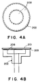
- Figure 4A is a top plan view
- Figure 4B is a sectional view
- the wafer 201 is placed on the top surface (contact surface) of the insulating layer 203, and a voltage is applied to the electrode 208. By the application of the voltage, an electrostatic force is produced to attract the wafer on the contact surface.
- a vacuum layer exists between the wafer and the contact surface of the apparatus with the result of significantly large resistance to the contact heat transfer.
- the resistance to the contact heat transfer between the wafer and wafer carrying surface is 10 -2 K.m 2 /W in the vacuum attraction, whereas it is 10 -4 K.m 2 /W in the electrostatic attraction, and therefore, the resistance is larger by approximately two orders in the vacuum attraction than in the electrostatic attraction.
- the heat produced in the wafer by absorption of exposure energy during the pattern transfer operation from the mask to the wafer is not easily released to the supporting apparatus in the vacuum attraction.
- the temperature rise of the wafer is a problem.
- the temperature rise of the mask as well as of the wafer is an additional problem. If the temperature of the mask rises, the pattern formed thereon is thermally deformed.
- a wafer supporting apparatus of the electrostatic attraction type when the electrode carrying the wafer on the attracting surface is supplied with the voltage, the attraction force is larger in the portion where the gap between the wafer and the attraction surface is smaller than where it is larger. Since the attraction force is smaller where the gap is large, the attraction force over the surface of the wafer is not uniform due to undulation. In some cases, the undulation is not corrected. In an extreme case, the wafer is demounted from the supporting apparatus.
- An object of the present invention is to provide a wafer supporting apparatus wherein the contact heat transfer resistance to the wafer is small, and wherein the wafer is positively and assuredly supported on the supporting surface.
- wafer supporting apparatus comprising a support structure having a supporting surface for supporting a wafer; vacuum attraction means for applying vacuum from a vacuum source to the rear side of the wafer to attract said wafer to said supporting surface; and electrostatic attraction means for attracting the wafer onto said supporting surface by electrostatic force; characterised by a pressure sensor connected to said vacuum attraction means, a valve for controlling the application of said vacuum source, and a control means adapted to operate in sequence said valve to apply vacuum to said wafer, to switch on said electrostatic attraction means, and to operate said valve to release said vacuum and to permit communication of the rear side of the wafer with ambient gas on receipt by said control means of a signal from said pressure sensor indicating that the pressure at the rear side of the wafer has reached a predetermined level.
- a method of supporting a wafer for the purpose of an exposure process comprising a) supporting the wafer on a support structure having vacuum attraction means and electrostatic attraction means, said vacuum attraction means and said electrostatic attraction means being controllable by control means and a pressure sensor, b) applying a vacuum to the rear side of the wafer by actuation of said vacuum attraction means by said control means for attracting the wafer onto the wafer supporting surface of said support structure until a predetermined pressure level is detected by said pressure sensor, c) actuating said electrostatic attraction means by said control means, d) thereafter de-activating said vacuum attraction means by said control means to release the vacuum, e) exposing the rear side of the wafer to ambient gas, and f) then applying exposure energy to the wafer while the latter is secured only by said electrostatic attraction means.
- the wafer is attracted by both of the vacuum attracting force and the electrostatic attracting force on the supporting surface. Thereafter, the vacuum attracting means is supplied with an ambient gas while the wafer continues to be attracted by the electrostatic attracting means, whereby the contact heat transfer resistance is reduced.
- Figure 1 is a top plan view of a wafer supporting apparatus according to an embodiment of the present invention.
- Figure 2A is a sectional view taken along a line A-A′ of Figure 1.
- Figure 2B is a sectional view taken along a line B-B′ of Figure 1.
- Figure 3A is a top plan view of a conventional vacuum attraction type wafer supporting means.
- Figure 3B is a sectional view of the apparatus of Figure 3.
- Figure 4A is a top plan view of a wafer supporting apparatus of a conventional electrostatic attraction wafer supporting apparatus.
- Figure 4B is a sectional view of an apparatus of Figure 1.
- the wafer supporting apparatus is shown as being used with a semiconductor exposure apparatus, although not shown, wherein a mask and a wafer are disposed in a vacuum ambience or a pressure-reduced ambience, and wherein a predetermined exposure energy such as X-rays contained in a synchrotron radiation beam is projected through the mask to the wafer, by which the pattern formed in the mask is transferred onto the wafer.
- a predetermined exposure energy such as X-rays contained in a synchrotron radiation beam
- a reference numeral 1 designated a semiconductor wafer onto which the pattern of the mask is to be transferred or printed.
- the wafer supporting apparatus of this embodiment includes a wafer supporting main assembly 2 for supporting the wafer 1 at an exposure position where the mask pattern is transferred thereonto and an insulating layer 3 constituting a contact surface with the wafer 1.
- the main assembly 2 is made of ceramic material such as Al 2 O 3 or SiC or metal such as SUS, Al.
- the insulating layer 3 is made of a material having high dielectric constant such as Al 2 O 3 . The thickness thereof is approximately 50 - 400 microns (micrometers). If the thickness of the insulating layer 3 is smaller, the electrostatic attraction force is larger.
- the top surface of the insulating layer 3 is formed into a contact surface 20 for contact with the wafer 1.
- the contact surface 20 is provided with vacuum attraction grooves 4 as shown in Figure 1 in the form of concentric circles.
- the vacuum attraction grooves 4 communicate with vacuum source 21 through a vacuum pipe 14.
- the vacuum pipe 14 is provided adjacent to the main assembly 2 with a pressure sensor 6 for detecting the pressure in the pipe 14. Between the pressure sensor 6 and the vacuum source 21, there is disposed a three way valve 7, by which the ambient gas or gases around the apparatus 24 can be introduced through a gas inlet 24 into the pipe at the pressure sensor 6 side.
- an electrode 8 is electrically connected to a high voltage source 10 through a switch 9. By closing the switch 9, a high voltage is applied to the electrode 8, by which an electrostatic force is produced between the apparatus and the wafer 1. Thus, the wafer is attracted and fixed on the insulating layer 3.
- an additional insulating layer provided on the bottom surface of the electrode 8.
- a water circulation region 11 is formed for circulating temperature control liquid (water) (temperature control medium).
- water temperature control liquid
- the cooling water controlled in its temperature at a predetermined level is supplied from a temperature controlled water source 23.
- the cooling water flows through the circulation region 11 to absorb the heat from the main assembly 2 and the wafer 1, and thereafter, is discharged through an outlet 13.
- the temperature-controlled water source 23 is controlled in its temperature in response to instructions from a controller 22, and also is controlled in the flow rate.
- the wafer is attracted in the following steps:
- the ambient gas around the main assembly 2 is introduced into the vacuum pipe 14 after the wafer is electrostatically attracted.
- a gas supplying source is connected the gas inlet 24 to introduce another gas or gases into the pipe 14.
- the ambient gas has relatively low thermal conductivity, such as air or nitrogen, it is possible that a highly thermally conductive gas such as He can be introduced into the vacuum pipe 14 from the gas inlet 24, by which the resistance to the contact heat transfer between the wafer 1 and the main assembly 2 of the supporting apparatus can be reduced.
- the wafer supporting means is provided with vacuum attraction means and electrostatic attraction means, by which the wafer can be assuredly retained and fixed on the wafer supporting surface.
- the undulation of the wafer can be corrected along the attracting surface of the supporting apparatus.
- the temperature rise of the wafer during the exposure operation of the wafer to the mask pattern can be suppressed. Therefore, the heat of the mask and the wafer can be removed efficiently, thus minimizing the thermal deformation of the mask pattern.
Landscapes
- Health & Medical Sciences (AREA)
- General Physics & Mathematics (AREA)
- Physics & Mathematics (AREA)
- Toxicology (AREA)
- Engineering & Computer Science (AREA)
- Environmental & Geological Engineering (AREA)
- Epidemiology (AREA)
- Public Health (AREA)
- Atmospheric Sciences (AREA)
- Life Sciences & Earth Sciences (AREA)
- Exposure Of Semiconductors, Excluding Electron Or Ion Beam Exposure (AREA)
- Exposure And Positioning Against Photoresist Photosensitive Materials (AREA)
- Container, Conveyance, Adherence, Positioning, Of Wafer (AREA)
Claims (9)
- Plättchentragvorrichtung, mit einer Tragestruktur mit einer Tragefläche zum Tragen eines Plättchens; einer Unterdruck-Anziehungseinrichtung (4, 7, 14, 21) zum Aufbringen eines Unterdrucks von einer Unterdruckquelle auf die Rückseite eines Plättchens, um das Plättchen an der Tragefläche anzuziehen; und einer elektrostatischen Anziehungseinrichtung (8, 9, 10) zum Anziehen des Plättchens auf der Tragefläche durch elektrostatische Kraft; gekennzeichnet durch einen mit der Unterdruck-Anziehungseinrichtung verbundenen Drucksensor (6), ein Ventil (7) zur Steuerung des Anlegens der Unterdruckquelle, und eine Steuereinrichtung (22), die geeignet ist, um aufeinanderfolgend das Ventil (7) anzusteuern, um Unterdruck auf das Plättchen aufzubringen, die elektrostatische Anziehungseinrichtung einzuschalten, und das Ventil (7) zu betätigen, um den Unterdruck abzulassen und eine Verbindung der Rückseite des Plättchens mit Umgebungsgas zuzulassen beim Empfang eines Signals von dem Drucksensor (6) durch die Steuereinrichtung, das angibt, daß der Druck an der Rückseite des Plättchens ein vorbestimmtes Niveau erreicht hat.
- Vorrichtung nach Anspruch 1, dadurch gekennzeichnet, daß die Unterdruck-Anziehungseinrichtung Nuten (4), die auf der Tragefläche ausgebildet sind, eine Unterdruckquelle (21) zum Aufbringen von Unterdruck in den Nuten und einen Gaseinlaß (14) zum Zuführen eines Gases in die Nuten (4) aufweist.
- Vorrichtung nach Anspruch 1 oder 2, gekennzeichnet durch eine Temperaturregeleinrichtung (11, 23) zum Zirkulieren eines temperaturgeregelten Mediums in der Tragestruktur.
- Vorrichtung nach Anspruch 3, dadurch gekennzeichnet, daß die Steuereinrichtung (22) auch die Temperaturregeleinrichtung (11, 23) steuert.
- Belichtungsvorrichtung mit Einrichtungen zum Aufbringen von Belichtungsenergie auf und durch eine Maske, wodurch ein in der Maske ausgebildetes Muster auf das Plättchen übertragen wird, mit einer Plättchentragvorrichtung nach einem der Ansprüche 1 bis 4.
- Verfahren zum Halten eines Plättchens für einen Belichtungsprozess, mit a) Tragen des Plättchens auf einer Tragevorrichtung mit einer Unterdruck-Anziehungseinrichtung und elektrostatischer Anziehungseinrichtung, wobei die Unterdruck-Anziehungseinrichtung und die elektrostatische Anziehungseinrichtung mittels einer Steuereinrichtung (22) und eines Drucksensors (6) steuerbar sind, b) Aufbringen eines Unterdrucks auf die Rückseite des Plättchens durch Betätigen der Unterdruck-Anziehungseinrichtung durch die Steuereinrichtung zum Anziehen des Plättchens an die Tragefläche der Tragestruktur bis ein vorbestimmtes Druckniveau von dem Drucksensor erfaßt wird, c) Betätigen der elektrostatischen Anziehungseinrichtung durch die Steuereinrichtung, d) danach Abschalten der Unterdruck-Anziehungseinrichtung durch die Steuereinrichtung, um den Unterdruck abzulassen, e) Aussetzen der Rückseite des Plättchens dem Umgebungsgas, und f) dann Aufbringen vom Belichtungsenergie auf das Plättchen, während letzteres nur von der elektrostatischen Anziehungseinrichtung gesichert ist.
- Verfahren nach Anspruch 6, dadurch gekennzeichnet, daß die Steuereinrichtung (22) aufeinanderfolgend ein Ventil (7) steuert, um den Unterdruck in Nuten (4), die in der Tragefläche der Tragestruktur ausgebildet sind aufzubringen, und um das Gas durch einen Gaseinlaß (24) in die Nuten einzuführen, nachdem die elektrostatische Anziehungseinrichtung betätigt ist.
- Verfahren nach Anspruch 6 oder 7, dadurch gekennzeichnet, daß die Temperatur der Tragestruktur durch ein die Tragestruktur passierendes temperaturgeregeltes Medium geregelt wird.
- Verfahren zum Belichten eines Plättchens mit den Schritten zum Halten des Plättchens unter Verwendung des Verfahrens nach einem der Ansprüche 6 bis 8 und Aufbringen von Belichtungsenergie auf und durch eine Maske, um ein auf der Maske ausgebildetes Muster auf das Plättchen zu übertragen.
Applications Claiming Priority (2)
| Application Number | Priority Date | Filing Date | Title |
|---|---|---|---|
| JP63218521A JP2748127B2 (ja) | 1988-09-02 | 1988-09-02 | ウエハ保持方法 |
| JP218521/88 | 1988-09-02 |
Publications (3)
| Publication Number | Publication Date |
|---|---|
| EP0357424A2 EP0357424A2 (de) | 1990-03-07 |
| EP0357424A3 EP0357424A3 (de) | 1990-10-17 |
| EP0357424B1 true EP0357424B1 (de) | 1996-10-23 |
Family
ID=16721236
Family Applications (1)
| Application Number | Title | Priority Date | Filing Date |
|---|---|---|---|
| EP89308822A Expired - Lifetime EP0357424B1 (de) | 1988-09-02 | 1989-08-31 | Plättchentragvorrichtung |
Country Status (4)
| Country | Link |
|---|---|
| US (1) | US4969168A (de) |
| EP (1) | EP0357424B1 (de) |
| JP (1) | JP2748127B2 (de) |
| DE (1) | DE68927364T2 (de) |
Cited By (1)
| Publication number | Priority date | Publication date | Assignee | Title |
|---|---|---|---|---|
| US7196775B2 (en) | 2004-08-23 | 2007-03-27 | Asml Holding N.V. | Patterned mask holding device and method using two holding systems |
Families Citing this family (53)
| Publication number | Priority date | Publication date | Assignee | Title |
|---|---|---|---|---|
| JPH0276212A (ja) * | 1988-09-13 | 1990-03-15 | Canon Inc | 多重露光方法 |
| JP2731950B2 (ja) * | 1989-07-13 | 1998-03-25 | キヤノン株式会社 | 露光方法 |
| EP0422814B1 (de) * | 1989-10-02 | 1999-03-17 | Canon Kabushiki Kaisha | Belichtungsvorrichtung |
| JPH03273663A (ja) * | 1990-03-23 | 1991-12-04 | Canon Inc | 基板保持装置 |
| EP0463853B1 (de) * | 1990-06-29 | 1998-11-04 | Canon Kabushiki Kaisha | Platte zum Arbeiten unter Vakuum |
| EP0779648A3 (de) * | 1990-07-02 | 1997-07-23 | Hitachi, Ltd. | Vakuum-Behandlungsverfahren und Vorrichtung |
| JP2748181B2 (ja) * | 1990-07-26 | 1998-05-06 | キヤノン株式会社 | ウエハチャック |
| JPH04162610A (ja) * | 1990-10-26 | 1992-06-08 | Canon Inc | マスク保持装置 |
| JP3004045B2 (ja) * | 1990-11-19 | 2000-01-31 | 株式会社東芝 | 露光装置 |
| US5203547A (en) * | 1990-11-29 | 1993-04-20 | Canon Kabushiki Kaisha | Vacuum attraction type substrate holding device |
| JPH04206948A (ja) * | 1990-11-30 | 1992-07-28 | Kyocera Corp | 静電チャック |
| JP3168018B2 (ja) * | 1991-03-22 | 2001-05-21 | キヤノン株式会社 | 基板吸着保持方法 |
| US5088006A (en) * | 1991-04-25 | 1992-02-11 | International Business Machines Corporation | Liquid film interface cooling system for semiconductor wafer processing |
| US5186238A (en) * | 1991-04-25 | 1993-02-16 | International Business Machines Corporation | Liquid film interface cooling chuck for semiconductor wafer processing |
| US5155652A (en) * | 1991-05-02 | 1992-10-13 | International Business Machines Corporation | Temperature cycling ceramic electrostatic chuck |
| DE4116392C2 (de) * | 1991-05-18 | 2001-05-03 | Micronas Gmbh | Halterung zur einseitigen Naßätzung von Halbleiterscheiben |
| EP0532236B1 (de) * | 1991-09-07 | 1997-07-16 | Canon Kabushiki Kaisha | System zur Stabilisierung der Formen von optischen Elementen, Belichtungsvorrichtung unter Verwendung dieses Systems und Verfahren zur Herstellung von Halbleitervorrichtungen |
| JP3224157B2 (ja) * | 1992-03-31 | 2001-10-29 | キヤノン株式会社 | X線マスクとその製造方法、並びに該x線マスクを用いたデバイス製造方法とx線露光装置 |
| JP2851766B2 (ja) * | 1993-04-28 | 1999-01-27 | 京セラ株式会社 | 静電チャック |
| TW277139B (de) * | 1993-09-16 | 1996-06-01 | Hitachi Seisakusyo Kk | |
| US6544379B2 (en) | 1993-09-16 | 2003-04-08 | Hitachi, Ltd. | Method of holding substrate and substrate holding system |
| US5593800A (en) * | 1994-01-06 | 1997-01-14 | Canon Kabushiki Kaisha | Mask manufacturing method and apparatus and device manufacturing method using a mask manufactured by the method or apparatus |
| US5548470A (en) * | 1994-07-19 | 1996-08-20 | International Business Machines Corporation | Characterization, modeling, and design of an electrostatic chuck with improved wafer temperature uniformity |
| US5854819A (en) * | 1996-02-07 | 1998-12-29 | Canon Kabushiki Kaisha | Mask supporting device and correction method therefor, and exposure apparatus and device producing method utilizing the same |
| US5828070A (en) * | 1996-02-16 | 1998-10-27 | Eaton Corporation | System and method for cooling workpieces processed by an ion implantation system |
| JP3814359B2 (ja) * | 1996-03-12 | 2006-08-30 | キヤノン株式会社 | X線投影露光装置及びデバイス製造方法 |
| JP3695000B2 (ja) * | 1996-08-08 | 2005-09-14 | 株式会社ニコン | 露光方法及び露光装置 |
| JP3372782B2 (ja) * | 1996-10-04 | 2003-02-04 | キヤノン株式会社 | 走査ステージ装置および走査型露光装置 |
| US5885428A (en) * | 1996-12-04 | 1999-03-23 | Applied Materials, Inc. | Method and apparatus for both mechanically and electrostatically clamping a wafer to a pedestal within a semiconductor wafer processing system |
| JP3178517B2 (ja) * | 1998-03-05 | 2001-06-18 | 日本電気株式会社 | パターン露光装置用試料台 |
| JP2000311933A (ja) | 1999-04-27 | 2000-11-07 | Canon Inc | 基板保持装置、基板搬送システム、露光装置、塗布装置およびデバイス製造方法ならびに基板保持部クリーニング方法 |
| JP2000349004A (ja) | 1999-06-03 | 2000-12-15 | Canon Inc | 位置決め装置、雰囲気置換方法、露光装置およびデバイス製造方法 |
| JP3492325B2 (ja) | 2000-03-06 | 2004-02-03 | キヤノン株式会社 | 画像表示装置の製造方法 |
| JP3869999B2 (ja) | 2000-03-30 | 2007-01-17 | キヤノン株式会社 | 露光装置および半導体デバイス製造方法 |
| EP1254606A1 (de) | 2001-05-04 | 2002-11-06 | Philip Morris Products S.A. | Einrichtung und Verfahren zum Lösen von Tabakballen |
| US20040187787A1 (en) * | 2003-03-31 | 2004-09-30 | Dawson Keith E. | Substrate support having temperature controlled substrate support surface |
| JP4227865B2 (ja) * | 2003-08-12 | 2009-02-18 | 株式会社ディスコ | プラズマエッチング方法及びプラズマエッチング装置 |
| JP3894562B2 (ja) * | 2003-10-01 | 2007-03-22 | キヤノン株式会社 | 基板吸着装置、露光装置およびデバイス製造方法 |
| US7245357B2 (en) * | 2003-12-15 | 2007-07-17 | Asml Netherlands B.V. | Lithographic apparatus and device manufacturing method |
| US8749762B2 (en) * | 2004-05-11 | 2014-06-10 | Asml Netherlands B.V. | Lithographic apparatus and device manufacturing method |
| JP2006245157A (ja) * | 2005-03-02 | 2006-09-14 | Canon Inc | 露光方法及び露光装置 |
| JP4692276B2 (ja) * | 2005-12-28 | 2011-06-01 | ウシオ電機株式会社 | 支持機構及び支持機構を使ったマスクステージ |
| US8469342B2 (en) * | 2007-07-23 | 2013-06-25 | Creative Technology Corporation | Substrate suction apparatus and method for manufacturing the same |
| US9130484B2 (en) | 2011-10-19 | 2015-09-08 | Sri International | Vacuum augmented electroadhesive device |
| US8982531B2 (en) * | 2011-10-19 | 2015-03-17 | Sri International | Additional force augmented electroadhesion |
| CN103367216A (zh) * | 2012-03-26 | 2013-10-23 | 上海宏力半导体制造有限公司 | 一种导水管和带有导水管的静电吸盘 |
| KR101578332B1 (ko) | 2012-07-26 | 2015-12-16 | 센주긴조쿠고교 가부시키가이샤 | 반도체 웨이퍼 반송 지그 |
| NL2013676A (en) * | 2014-02-11 | 2015-08-17 | Asml Netherlands Bv | A method of clamping articles for a lithographic apparatus, a controller for a lithographic apparatus, a chuck, a method of using a chuck and a device manufacturing method. |
| JP2019075477A (ja) * | 2017-10-17 | 2019-05-16 | 株式会社ディスコ | チャックテーブル機構 |
| US20200251357A1 (en) * | 2019-02-01 | 2020-08-06 | Edwards Limited | Method and apparatus for supplying gas to a chuck |
| US11196360B2 (en) * | 2019-07-26 | 2021-12-07 | Applied Materials, Inc. | System and method for electrostatically chucking a substrate to a carrier |
| CN112068402B (zh) * | 2020-09-09 | 2022-04-22 | 江西芯光微电子有限公司 | 一种用于光刻机的晶片吸盘 |
| CN118571823B (zh) * | 2023-12-06 | 2025-08-15 | 拓荆创益(沈阳)半导体设备有限公司 | 一种晶圆托盘及薄膜沉积装置 |
Family Cites Families (8)
| Publication number | Priority date | Publication date | Assignee | Title |
|---|---|---|---|---|
| US3711081A (en) * | 1970-03-31 | 1973-01-16 | Ibm | Semiconductor wafer chuck |
| JPS6013740U (ja) * | 1983-07-06 | 1985-01-30 | 日本電子株式会社 | 試料保持装置 |
| JPS6099538A (ja) * | 1983-11-01 | 1985-06-03 | 横河・ヒュ−レット・パッカ−ド株式会社 | ピンチヤツク |
| JPS61192435A (ja) * | 1985-02-21 | 1986-08-27 | Canon Inc | 静電吸着保持装置 |
| JPS6289337A (ja) * | 1985-10-16 | 1987-04-23 | Canon Inc | 吸着装置 |
| JPS62277234A (ja) * | 1986-05-23 | 1987-12-02 | Canon Inc | 静電チヤツク装置 |
| JPS6372877A (ja) * | 1986-09-12 | 1988-04-02 | Tokuda Seisakusho Ltd | 真空処理装置 |
| JP2649519B2 (ja) * | 1987-07-21 | 1997-09-03 | キヤノン株式会社 | 平板状物体移送位置決め装置 |
-
1988
- 1988-09-02 JP JP63218521A patent/JP2748127B2/ja not_active Expired - Fee Related
-
1989
- 1989-08-31 US US07/401,654 patent/US4969168A/en not_active Expired - Lifetime
- 1989-08-31 EP EP89308822A patent/EP0357424B1/de not_active Expired - Lifetime
- 1989-08-31 DE DE68927364T patent/DE68927364T2/de not_active Expired - Fee Related
Cited By (1)
| Publication number | Priority date | Publication date | Assignee | Title |
|---|---|---|---|---|
| US7196775B2 (en) | 2004-08-23 | 2007-03-27 | Asml Holding N.V. | Patterned mask holding device and method using two holding systems |
Also Published As
| Publication number | Publication date |
|---|---|
| US4969168A (en) | 1990-11-06 |
| EP0357424A3 (de) | 1990-10-17 |
| JP2748127B2 (ja) | 1998-05-06 |
| JPH0267745A (ja) | 1990-03-07 |
| DE68927364T2 (de) | 1997-03-06 |
| EP0357424A2 (de) | 1990-03-07 |
| DE68927364D1 (de) | 1996-11-28 |
Similar Documents
| Publication | Publication Date | Title |
|---|---|---|
| US4969168A (en) | Wafer supporting apparatus | |
| EP0320297B1 (de) | Verfahren zur Temperaturkontrolle einer Halbleiterscheibe auf einer Einspannvorrichtung | |
| KR100431658B1 (ko) | 기판 가열 장치 및 이를 갖는 장치 | |
| US5738165A (en) | Substrate holding apparatus | |
| JP4149002B2 (ja) | 静電チャックおよび物体の温度をプラズマ処理中制御する方法 | |
| US7731798B2 (en) | Heated chuck for laser thermal processing | |
| JP4397271B2 (ja) | 処理装置 | |
| US7372690B2 (en) | Substrate holder which is self-adjusting for substrate deformation | |
| EP0325243A2 (de) | Ätzgerät | |
| KR20060071852A (ko) | 히터 장착 정전 척 | |
| JPH11168056A (ja) | ウェハ保持装置 | |
| CN112309816B (zh) | 基板支承装置和包括基板支承装置的基板处理装置 | |
| JP3106499B2 (ja) | 露光装置 | |
| JP4364105B2 (ja) | 熱処理装置、及び熱処理方法 | |
| JP4004637B2 (ja) | 静電チャック、加熱冷却装置、加熱冷却方法及び真空処理装置 | |
| JP7556320B2 (ja) | 基板取り外し装置 | |
| JP3898895B2 (ja) | 加熱処理装置及び加熱処理方法 | |
| US20250022739A1 (en) | Process system, method, and substrate chuck | |
| JP2719332B2 (ja) | プラズマ処理方法 | |
| JPH04371579A (ja) | 静電吸着装置 | |
| KR102680635B1 (ko) | 냉각 유닛과 이를 포함하는 열처리 장치 및 열처리 방법 | |
| JPH037883A (ja) | 薄膜加熱装置 | |
| KR100284669B1 (ko) | 열전 반도체를 이용한 정전척의 표면온도 제어시스템 | |
| JPH08243915A (ja) | 化学的機械研磨装置 | |
| JP4851449B2 (ja) | 熱回路を有するウェーハ及びその電気供給システム |
Legal Events
| Date | Code | Title | Description |
|---|---|---|---|
| PUAI | Public reference made under article 153(3) epc to a published international application that has entered the european phase |
Free format text: ORIGINAL CODE: 0009012 |
|
| AK | Designated contracting states |
Kind code of ref document: A2 Designated state(s): DE FR GB NL |
|
| PUAL | Search report despatched |
Free format text: ORIGINAL CODE: 0009013 |
|
| AK | Designated contracting states |
Kind code of ref document: A3 Designated state(s): DE FR GB NL |
|
| 17P | Request for examination filed |
Effective date: 19901231 |
|
| 17Q | First examination report despatched |
Effective date: 19920911 |
|
| GRAH | Despatch of communication of intention to grant a patent |
Free format text: ORIGINAL CODE: EPIDOS IGRA |
|
| GRAH | Despatch of communication of intention to grant a patent |
Free format text: ORIGINAL CODE: EPIDOS IGRA |
|
| GRAA | (expected) grant |
Free format text: ORIGINAL CODE: 0009210 |
|
| AK | Designated contracting states |
Kind code of ref document: B1 Designated state(s): DE FR GB NL |
|
| REF | Corresponds to: |
Ref document number: 68927364 Country of ref document: DE Date of ref document: 19961128 |
|
| ET | Fr: translation filed | ||
| PLBE | No opposition filed within time limit |
Free format text: ORIGINAL CODE: 0009261 |
|
| STAA | Information on the status of an ep patent application or granted ep patent |
Free format text: STATUS: NO OPPOSITION FILED WITHIN TIME LIMIT |
|
| 26N | No opposition filed | ||
| REG | Reference to a national code |
Ref country code: GB Ref legal event code: IF02 |
|
| PGFP | Annual fee paid to national office [announced via postgrant information from national office to epo] |
Ref country code: DE Payment date: 20070831 Year of fee payment: 19 |
|
| PGFP | Annual fee paid to national office [announced via postgrant information from national office to epo] |
Ref country code: GB Payment date: 20070813 Year of fee payment: 19 |
|
| PGFP | Annual fee paid to national office [announced via postgrant information from national office to epo] |
Ref country code: NL Payment date: 20070816 Year of fee payment: 19 |
|
| PGFP | Annual fee paid to national office [announced via postgrant information from national office to epo] |
Ref country code: FR Payment date: 20070820 Year of fee payment: 19 |
|
| GBPC | Gb: european patent ceased through non-payment of renewal fee |
Effective date: 20080831 |
|
| NLV4 | Nl: lapsed or anulled due to non-payment of the annual fee |
Effective date: 20090301 |
|
| PG25 | Lapsed in a contracting state [announced via postgrant information from national office to epo] |
Ref country code: NL Free format text: LAPSE BECAUSE OF NON-PAYMENT OF DUE FEES Effective date: 20090301 |
|
| REG | Reference to a national code |
Ref country code: FR Ref legal event code: ST Effective date: 20090430 |
|
| PG25 | Lapsed in a contracting state [announced via postgrant information from national office to epo] |
Ref country code: FR Free format text: LAPSE BECAUSE OF NON-PAYMENT OF DUE FEES Effective date: 20080901 Ref country code: DE Free format text: LAPSE BECAUSE OF NON-PAYMENT OF DUE FEES Effective date: 20090303 |
|
| PG25 | Lapsed in a contracting state [announced via postgrant information from national office to epo] |
Ref country code: GB Free format text: LAPSE BECAUSE OF NON-PAYMENT OF DUE FEES Effective date: 20080831 |