EP0357434B1 - Appareil de formation d'images - Google Patents
Appareil de formation d'images Download PDFInfo
- Publication number
- EP0357434B1 EP0357434B1 EP89308835A EP89308835A EP0357434B1 EP 0357434 B1 EP0357434 B1 EP 0357434B1 EP 89308835 A EP89308835 A EP 89308835A EP 89308835 A EP89308835 A EP 89308835A EP 0357434 B1 EP0357434 B1 EP 0357434B1
- Authority
- EP
- European Patent Office
- Prior art keywords
- developer
- photoconductor drum
- image forming
- forming apparatus
- developer unit
- Prior art date
- Legal status (The legal status is an assumption and is not a legal conclusion. Google has not performed a legal analysis and makes no representation as to the accuracy of the status listed.)
- Expired - Lifetime
Links
Images




Classifications
-
- G—PHYSICS
- G03—PHOTOGRAPHY; CINEMATOGRAPHY; ANALOGOUS TECHNIQUES USING WAVES OTHER THAN OPTICAL WAVES; ELECTROGRAPHY; HOLOGRAPHY
- G03G—ELECTROGRAPHY; ELECTROPHOTOGRAPHY; MAGNETOGRAPHY
- G03G15/00—Apparatus for electrographic processes using a charge pattern
- G03G15/06—Apparatus for electrographic processes using a charge pattern for developing
- G03G15/08—Apparatus for electrographic processes using a charge pattern for developing using a solid developer, e.g. powder developer
- G03G15/09—Apparatus for electrographic processes using a charge pattern for developing using a solid developer, e.g. powder developer using magnetic brush
-
- G—PHYSICS
- G03—PHOTOGRAPHY; CINEMATOGRAPHY; ANALOGOUS TECHNIQUES USING WAVES OTHER THAN OPTICAL WAVES; ELECTROGRAPHY; HOLOGRAPHY
- G03G—ELECTROGRAPHY; ELECTROPHOTOGRAPHY; MAGNETOGRAPHY
- G03G15/00—Apparatus for electrographic processes using a charge pattern
- G03G15/06—Apparatus for electrographic processes using a charge pattern for developing
- G03G15/08—Apparatus for electrographic processes using a charge pattern for developing using a solid developer, e.g. powder developer
- G03G15/0896—Arrangements or disposition of the complete developer unit or parts thereof not provided for by groups G03G15/08 - G03G15/0894
- G03G15/0898—Arrangements or disposition of the complete developer unit or parts thereof not provided for by groups G03G15/08 - G03G15/0894 for preventing toner scattering during operation, e.g. seals
-
- G—PHYSICS
- G03—PHOTOGRAPHY; CINEMATOGRAPHY; ANALOGOUS TECHNIQUES USING WAVES OTHER THAN OPTICAL WAVES; ELECTROGRAPHY; HOLOGRAPHY
- G03G—ELECTROGRAPHY; ELECTROPHOTOGRAPHY; MAGNETOGRAPHY
- G03G15/00—Apparatus for electrographic processes using a charge pattern
- G03G15/01—Apparatus for electrographic processes using a charge pattern for producing multicoloured copies
- G03G15/0105—Details of unit
- G03G15/0126—Details of unit using a solid developer
Definitions
- the present invention relates to an image forming apparatus such as an electrophotographic copying machine or the like, for forming an image by developing a latent image formed on a photoconductor drum with developer delivered from a developer unit. More particularly, the invention relates to an image forming apparatus wherein the scattering of developer falling through the clearance between the photoconductor drum and the developer unit is resisted.
- an electrostatic latent image is formed, as shown in Fig. 7 on a photoconductor drum 51 (rotating in the clockwise direction as shown by the arrow B in the drawing), the electrostatic latent image then being developed with developer delivered from a developer unit 60, after which the image formed on the photoconductor drum 51 is transferred to copy paper to form a copy image.
- the developer unit 60 is provided with a developing sleeve 61 (rotating in the counterclockwise direction as shown by the arrow A in the drawing), which is disposed in a housing 62 and in a location facing the photoconductor drum 51, the developing sleeve 61 having a magnetic brush formed thereon to carry developer to the photoconductor drum 51.
- the housing 62 of the developer unit 60 is so disposed that a slight clearance is created with respect to the photoconductor drum 51 .
- part of the developer being carried by the magnetic brush provided on the circumferential surface of the developing sleeve 61 may fall downward through the clearance between the photoconductor drum 51 and the housing 62 to be scattered in a copy paper conveyance path beneath the developer unit 60 .
- the developer scattered in the copy paper conveyance path will adhere to the copy paper conveyed thereto and therefore stain the copy paper. If an image is transferred to the stained copy paper, the transferred image will come out blurred.
- a developer collecting member 80 for collecting the developer falling through the clearance between the photoconductor drum 51 and the housing 62 of the developer unit 60 is disposed beneath the position at which the photoconductor drum 51 faces the developer unit 60 .
- the photoconductor drum 51 is rotatably supported between a pair of photoconductor drum supporting side plates 52 , each having in the lower part thereof a supporting portion 52a so formed as to protrude toward the developer unit.
- the developer collecting member 80 is so mounted as to stretch between the supporting portions 52a of the photoconductor drum supporting side plates 52 , each end thereof being secured to the corresponding supporting portion 52a with a screw 82 or the like.
- the developer falling from between the photoconductor drum 51 and the developer unit 60 is collected on the developer collecting member 80 , thus preventing the developer from being scattered in the copy paper conveyance path beneath the developer collecting member 80 .
- the developer collecting member 80 is formed from sheet metal into such a shape as to prevent the collected developer from dropping. Since the developer collecting member 80 is formed from such sheet metal, when each end of the developer collecting member 80 is secured to the supporting portion 52a of the corresponding photoconductor drum supporting side plate 52 by a screw 82 , the entire developer collecting member 80 may be twisted depending on the tightening condition of the screw 82 . If the developer collecting member 80 is mounted in a twisted state, the pair of photoconductor drum supporting side plates 52 may be disaligned with each other, and the photoconductor drum 51 may not be properly supported between the photoconductor drum supporting side plates 52 .
- the photoconductor drum 51 may not be properly positioned with respect to the developer unit 60 . If the photoconductor drum 51 is not properly positioned with respect to the developer unit 60 , the electrostatic latent image on the photoconductor drum 51 will not be developed by the developer unit 60 .
- image forming apparatuses that are capable of forming a multi-color image using developers of different colors such as black and red.
- Some of such image forming apparatuses comprise, as shown in Fig. 8, a main developer unit 60 for developing an electrostatic latent image on the photoconductor drum 51 , for example, with a black developer, and a sub developer unit 70 for developing the latent image on the photoconductor drum 51 , for example, with a red developer, the sub developer unit 70 being disposed above the main developer unit 60 , both facing the photoconductor drum 51 (rotating in direction B ).
- the main developer unit 60 and the sub developer unit 70 are respectively provided with developing sleeves (rotating in direction A ) 61 and 71 disposed in respective housings 62 and 72 and facing the photoconductor drum 51 , the housings 62 and 72 being swingable about respective fulcrums 63 and 73 to move the respective developing sleeves 61 and 71 close to and away from the photoconductor drum 51 .
- the developing sleeves 61 and 71 are moved close to the photoconductor drum 51 and positioned in the developing position, the developer units 60 and 70 develop the latent image on the photoconductor drum using the developing sleeves 61 and 71 .
- the developer units 60 and 70 do not develop the latent image on the photoconductor drum 51 , the developing sleeves 61 and 71 being inoperative.
- developer collecting members 81 and 81 are disposed, one beneath the position at which the main developer unit 60 faces the photoconductor drum 51 and the other beneath the position at which the sub developer unit 70 faces the photoconductor drum 51 .
- the clearance is enlarged between the housings 62 and 72 of the developer units 60 and 70 and the respective developer collecting members 81 and 81 , the developer falling through the clearance between the photoconductor drum 51 and the developer units 60 and 70 will not be completely collected by the respective developer collecting members 81 and 81 , resulting in the scattering of developer below the developer collecting members 81 and 81 . Also, if the clearance is enlarged between the housings 62 and 72 of the developer units 60 and 70 and the respective developer collecting members 81 and 81 , air may flow through the clearance and cause the developer collected on the developer collecting members 81 to fly around.
- Providing larger size developer collecting members 81 may be considered to prevent the developer from scattering therebelow, even when the developer units 60 and 70 are positioned in the receding position away from the photoconductor drum 51 , but, since the clearance between the photoconductor drum 51 and the developer units 60 and 70 varies with the swinging motion of the developer units 60 and 70, it is not possible to completely prevent the developer from scattering downward with the provision of the developer collecting members 81 and 81.
- the image forming apparatus of this invention provides a generally improved device.
- an image forming apparatus for forming an image by developing a latent image on a photoconductor drum with developer delivered from a developer unit disposed facing the photoconductor drum, having developer collection means for collecting, in use, the developer falling from between the photoconductor drum and the developer unit, characterised in that a developer collecting member is disposed between, and integrally moulded with, a pair of photoconductor drum supporting side plates which rotatably support the photoconductor drum.
- the developer collecting member has an upwardly extending wall on the side near to the developer unit.
- the developer unit may be movable between a developing position close to the photoconductor drum and a retracted position away from the photoconductor drum and the developer collecting member may be provided with a flexible seal member which extends to the developer unit.
- the seal member may be attached to the outer surface, that is, the side nearest the developer unit, of the wall of the developer collecting member.
- the seal member may be attached to the inner surface, that is, the side nearest the photoconductor drum, of the wall of the developer collecting member.
- the seal member may be detachable from the developer collecting member.
- the seal member may be slidably connected to the developer unit by slide means to accommodate the movement of the developer unit towards and away from the photoconductor drum.
- the seal member may be detachably connected to the developer unit.
- the seal member may be attached to a mounting guide which is slidably mounted on and detached from the developer collecting member.
- the seal member may be slidably connected to a supporting guide which is detachable from the developer unit.
- the image forming apparatus may be provided with a plurality of developer units, the developer collecting members being disposed beneath the respective positions at which the developer units face the photoconductor drum.
- the invention described herein makes possible the objectives of (1) providing an image forming apparatus of the present invention in which a specified positional relationship is always provided between the photoconductor drum and the developer collecting member that collects the developer falling through the clearance between the photoconductor drum and the developer unit, and, accordingly the photoconductor drum is readily positioned in a specified position with respect to the developer unit; (2) providing an image forming apparatus in which the photoconductor drum is easily supported between the pair of photoconductor drum supporting side plates; (3) providing an image forming apparatus in which the developer falling from between the photoconductor drum and the developer unit is properly prevented by means of the seal member, from scattering below the developer unit even when the clearance changes between the photoconductor drum and the developer unit as the developer unit moves; (4) providing an image forming apparatus in which the sealing performance of the seal member is further improved by connecting it in such a way as to follow the movement of the developer unit; and (5) providing an image forming apparatus in which the seal member is easily replaceable by detachably attaching it to the developer collecting member
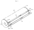
- Fig. 1 is a perspective view showing a photoconductor drum and its adjacent parts, with the photoconductor drum detached, of an image forming apparatus according to a first embodiment of the present invention.
- the developer unit (not shown) is disposed facing a photoconductor drum 51 , the developer unit being used to develop a latent image formed on the photoconductor drum 51 with developer.
- a developer collecting member 11 is disposed beneath the position at which the photoconductor drum 51 faces the developer unit (not shown).
- the developer collecting member 11 which collects the developer falling through the clearance between the photoconductor drum 51 and the developer unit is disposed in such a way as to connect a pair of photoconductor drum supporting side plates 52 which rotatably support the photoconductor drum 51 .
- Each photoconductor drum supporting side plate 52 is formed in a disc shape with a rotation shaft supporting hole 52a formed in the center thereof.
- each photoconductor drum supporting side plate 52 On the lower part of each photoconductor drum supporting side plate 52 is formed a supporting portion 52b which is disposed facing the photoconductor drum 51 and protruding toward the developer unit.
- the developer collecting member 11 is integrally molded with the photoconductor drum supporting plates 52 , using plastic, etc., the developer collecting member 11 being disposed to connect the two supporting portions 52b . Therefore, the two photoconductor drum supporting side plates 52 and the developer collecting member 11 combine to form an integrally molded frame-like construction, thus the photoconductor drum supporting side plates 52 being firmly connected with each other without going out of alignment with respect to each other.
- the developer collecting member 11 is a box-shape hollow construction with an open top, and the developer falling through the clearance between the photoconductor drum 51 and the developer unit is collected in the developer collecting member 11 .
- a flange 51a is fitted into each end of the photoconductor drum 51 , the flange 51a being provided with a rotation shaft mounting hole 51b formed in the center thereof.
- the photoconductor drum 51 is put into an assembly in the following manner. First, the photoconductor drum 51 is positioned between the two photoconductor drum supporting side plates 52 , and a rotation shaft 53 is put through the rotation shaft supporting hole 52a of one photoconductor drum supporting side plate 52 , to be inserted in the rotation shaft mounting holes 51b of the flanges 51a fitted to the photoconductor drum 51 . The rotation shaft 53 is then fixed to the flanges 51a , thus being made integrally rotatable with the photoconductor drum 51 . After that, the rotation shaft 53 is inserted in the rotation shaft supporting hole 52a of the other photoconductor drum supporting side plate 52 , thus being rotatably supported in the rotation shaft supporting holes 52a of the two photoconductor drum supporting side plates 52 .
- the photoconductor drum supporting side plates 52 are integrally molded with the developer collecting member 11 which firmly connects them together, the photoconductor drum 51 is able to be smoothly and quickly supported on the photoconductor drum supporting side plates 52 via the rotation shaft 53 . Since it is not necessary to use screws to fix the developer collecting member 11 to the photoconductor drum supporting side plates 52 , the assembling work efficiency of the photoconductor drum is further improved.
- An image forming apparatus in a second embodiments is provided, as shown in Fig. 2, with two developer units 60 and 70 .
- the developer units 60 and 70 are disposed one above the other, each facing the photoconductor drum 51 .
- the developer unit 60 in the lower position is used to develop a latent image on the photoconductor drum 51 , for example, with black developer.
- the sub developer unit 70 disposed above the main developer unit 60 is used to develop the latent image on the photoconductor drum 51 with a developer of a different color from the developer of the main developer unit 60 , for example, with red developer.
- the main developer unit 60 is provided in the housing 62 with a developing sleeve 61 disposed rotatably in the counterclockwise direction indicated by the arrow A in the drawing in a location facing the photoconductor drum 51 .
- the developing sleeve 61 is rotated to form a magnetic sleeve on its circumferential surface to carry developer.
- the main developer unit 60 is swingable about a fulcrum 63 between a developing position (indicated by a solid line in Fig. 2) and a receding position (indicated by a dash-dot line in Fig.
- the developing position being the position where the developing sleeve 61 is positioned close to the photoconductor drum 51 so that the developer on the magnetic brush contacts the photoconductor drum 51
- the receding position being the position where the developing sleeve 61 is positioned away from the photoconductor drum 51 so that the magnetic brush does not contact the photoconductor drum 51 .
- the sub developer unit 70 disposed above the main developer unit 60 is also provided in the housing 72 with a developing sleeve 71 disposed facing the photoconductor drum 51 the sub developer unit 70 being swingable about a fulcrum 73 in the same way as the main developer unit 60 between a developing position (indicated by a line of dashed and double dots in Fig. 2) where the developing sleeve 71 is positioned close to the photoconductor drum 51 and a receding position (indicated by a solid line in Fig. 2) where the developing sleeve 71 is positioned away from the photoconductor drum 51 . Either the main developer unit 60 or the sub developer unit 70 is selected, and moved to the developing position to develop the latent image on the photoconductor drum 51 .
- a developer collecting member 21 is disposed beneath the position at which the developing sleeve 61 of the main developer unit 60 faces the photoconductor drum 51 , while a developer collecting member 31 of a similar construction is disposed above the main developer unit 60 and beneath the position at which the developing sleeve 71 of the sub developer unit 70 faces the photoconductor drum 51 .
- the developer collecting members 21 and 31 are integrally molded with a pair of photoconductor drum supporting side plates 52 and 52 (Fig. 3). As shown in Fig. 3, the developer collecting members 21 and 31 are disposed respectively as connecting supporting portions 52d - 52d and 52e - 52e formed on the photoconductor drum supporting side plates 52 and protruding toward the main developer unit 60 and the sub developer unit 70 , respectively.
- the developer collecting members 21 and 31 are respectively provided with vertical wall portions 21a and 31a upwardly extending toward the side edge portions of the main developer unit 60 and the sub developer unit 70 respectively, the wall portions 21a and 31a being so disposed that they do not contact the housings 62 and 72 even when the main developer unit 60 and the sub developer unit 70 are moved to their respective receding positions.
- the seal members 22 and 32 are formed of a flexible material, the edge portions thereof respectively contacting the undersides of the respective housings 62 and 72 of the main developer unit 60 and the sub developer unit 70 .
- the respective seal members 22 and 32 are flexed to follow the movement of the developer units 60 and 70 with the edge portions thereof respectively contacting the undersides of the housings 62 and 72 .
- the respective seal members 22 and 32 flex by their own resilience to follow the movement of the developer units 60 and 70 with the edge portions thereof respectively contacting the undersides of the housings 62 and 72 .
- the seal members 22 and 32 Since the clearance between the photoconductor drum 51 and each of the main developer unit 60 and sub developer unit 70 is always sealed by the seal members 22 and 32 , the developer falling through the clearance is securely collected on the developer collecting members 21 and 31 without being scattered therebelow. Also, since the seal members 22 and 32 seal the clearance between the photoconductor drum 51 and each of the main developer unit 60 and sub developer unit 70 to block the circulation of air therethrough, there is no possibility that the developer collected on the developer collecting members 21 and 31 will fly around.
- the seal member 32 disposed beneath the sub developer unit 70 prevents the developer in the sub developer unit 70 from being scattered downward, and therefore prevents the developer in the sub developer unit 70 from getting mixed in the developer of different color in the main developer unit 60 disposed beneath the sub developer unit 70 , thus eliminating the possibility of deteriorating the color of the image developed by the main developer unit 60 .
- an image forming apparatus having two developer units has been described, but this embodiment is also applicable to one having three or more developer units, for example, a full-color image forming apparatus.
- This embodiment is also applicable to an image forming apparatus having a single developer.
- the developer units of the image forming apparatus according to this embodiment are so constructed that they move to the developing and receding positions by swinging motion, but alternatively, they may be constructed to achieve the same objects by reciprocal movement in parallel directions.
- An image forming apparatus in a third embodiment is provided, as shown in Fig. 4, with a main developer unit 60 and a sub developer unit 70 , like the foregoing second embodiment, each swingable between a developing position close to the photoconductor drum 51 and a receding position away therefrom.
- a developer collecting member 41 disposed beneath the main developer unit 60 is integrally molded with a pair of photoconductor drum supporting side plates 52 in the same way as the developer collecting members 21 and 31 in the second embodiment.
- the developer collecting member 41 is disposed in such a way as to connect the supporting portions 52d on the photoconductor drum supporting plates 52 , and is provided with an upwardly extending vertical wall portion 41a on the side edge thereof nearer to the main developer unit 20 .
- an outwardly open guide groove 41b is formed in the outer surface of the wall portion 41a of the developer collecting member 41 along the entire length thereof.
- a bar-like mounting guide 43 to which the base portion of the seal member 42 is fixed.
- the seal member 42 whose base portion is fixed to the mounting guide 43 has its entire center portion between the base portion and the edge portion supported by a supporting guide 44 .
- the supporting guide 44 is provided with a bar-like body 44b having a slit opening 44a into which the seal member 42 is slidably inserted and a guide portion 44c disposed above the body 44b and protruding from the sides of the body 44b .
- the guide portion 44c is slidably fitted in a guide groove 64 disposed on the underside of the housing 62 of the main developer unit 60 .
- the edge portion 42a of the seal member 42 is formed in a spherical shape so as to prevent it from being pulled out through the slit opening 44a in the body 44b of the supporting guide 44 .
- a developer collecting member 41 disposed beneath the sub developer unit 70 has the same construction as above, and a seal member 42 is also constructed in the same manner and attached to the developer collecting member 41 and the developer unit 70 .
- the seal members 42 in this embodiment prevent the developer falling from the clearance between the photoconductor drum 51 and the developer units 60 and 70 from being scattered downward, as well as the circulation of air therethrough. Since the seal members 42 in this embodiment are slidably connected to the respective developer units 60 and 70 , the seal members 42 properly move following the movement of the respective developer units 60 and 70 , when the developer units 60 and 70 are moved, thus improving the sealing effect between each of the developer units 60 and 70 and the photoconductor drum 51 . Also, since the seal members 42 are slidingly mounted on, and detached from the respective developer collecting members 41 , replacement of the seal members 42 is quite easy. Also, the seal members 42 are able to be removed when the developer units 60 and 70 are mounted in or detached from the apparatus, thus facilitating the mounting and detaching of the developer units 60 and 70 .
- this embodiment is also applicable to an image forming apparatus having three or more developer units, for example, to a full-color image forming apparatus, and is also applicable to an image forming apparatus having a single developer unit.
- the developer units may be so constructed, for example, that they move reciprocally in parallel directions.
- An image forming apparatus in a fourth embodiment has a construction, as shown in Fig. 6, such that a guide groove 41b is formed on the inner surface, the side nearer to the photoconductor drum 51 , of the wall portion 41a of the developer collecting member 41 , the base portion of the seal member 42 being detachably fitted in the guide groove 41b .
- the image forming apparatus in this embodiment has the same construction as that of the foregoing third embodiment.
Landscapes
- Physics & Mathematics (AREA)
- General Physics & Mathematics (AREA)
- Dry Development In Electrophotography (AREA)
- Electrophotography Configuration And Component (AREA)
Claims (11)
- Appareil de formation d'images pour former une image par développement d'une image latente sur un tambour photoconducteur (51) avec un révélateur délivré par une unité de développement (60, 61, 62) disposée en face du tambour photoconducteur, ayant des moyens de collecte du révélateur pour collecter, au cours de l'utilisation, le révélateur tombant entre le tambour photoconducteur (51) et l'unité de développement (60, 61, 62), caractérisé en ce qu'un dispositif de collecte du révélateur (11, 21, 31, 41) est disposé entre deux plaques latérales de support (52) du tambour photoconducteur et intégralement moulé avec elles, qui supportent le tambour photoconducteur, avec possibilité pour lui de se mouvoir en rotation.
- Appareil de formation d'images selon la revendication 1, caractérisé en ce que le dispositif de collecte du révélateur (11, 21, 31, 41) a une paroi s'étendant vers le haut sur le côté le plus proche de l'unité de développement.
- Appareil de formation d'images selon la revendication 1 ou 2, caractérisé en ce que l'unité de développement (60, 61, 62) est mobile entre une position de développement tout contre le tambour photoconducteur (51) et une position en retrait à l'écart du tambour photoconducteur (51) et le dispositif de collecte du révélateur (11, 21, 31, 41) est pourvu d'un élément d'étanchéité souple (22, 32, 42) qui s'étend jusqu'à l'unité de développement (60, 61, 62).
- Appareil de formation d'images selon la revendication 3, caractérisé en ce que l'élément d'étanchéité (22, 32, 42) est attaché à la surface extérieure (21a, 31a, 41a), c'est-à-dire, le côté de la paroi du dispositif de collecte du révélateur (11, 21, 31, 41) le plus proche de l'unité de développement.
- Appareil de formation d'images selon la revendication 3, caractérisé en ce que l'élément d'étanchéité (22, 32, 42) est attaché à la surface intérieure (41b), c'est-à-dire, le côté de la paroi du dispositif de collecte du révélateur (11, 21, 31, 41) le plus proche du tambour photoconducteur (51).
- Appareil de formation d'images selon la revendication 3, 4 ou 5, caractérisé en ce que l'élément d'étanchéité (22, 32, 42) est séparable du dispositif de collecte du révélateur (11, 21, 31, 41).
- Appareil de formation d'images selon la revendication 3, 4, 5 ou 6, caractérisé en ce que l'élément d'étanchéité (22, 32, 42) est relié à coulissement à l'unité de développement (60, 61, 62) par des moyens de coulissement (44, 44a, 44b, 44c) pour satisfaire au mouvement du révélateur vers le tambour photoconducteur (51) ou à l'écart de celui-ci.
- Appareil de formation d'images selon la revendication 7, caractérisé en ce que l'élément d'étanchéité (22, 32, 42, 44, 44a, 44b, 44c) est relié avec possibilité d'en être séparé à l'unité de développement (60, 61, 62).
- Appareil de formation d'images selon la revendication 4, caractérisé en ce que l'élément d'étanchéité (22, 32, 42) est attaché à un guide de montage (43) qui est monté sur le dispositif de collecte du révélateur (11, 21, 41) et en est séparé par coulissement.
- Appareil de formation d'images selon la revendication 3, caractérisé en ce que l'élément d'étanchéité (22, 32, 42) est relié à coulissement à un guide support (43) qui est séparable de l'unité de développement (60, 61, 62).
- Appareil de formation d'images selon l'une quelconque des revendications précédentes, caractérisé en ce que l'appareil de formation d'images est pourvu de plusieurs unités de développement (60, 61, 62, 70, 71, 72), le dispositif de collecte du révélateur (11, 21, 31, 41) étant disposé au-dessous des positions respectives où les unités de développement font face au tambour photoconducteur (51).
Applications Claiming Priority (6)
| Application Number | Priority Date | Filing Date | Title |
|---|---|---|---|
| JP114391/88 | 1988-08-31 | ||
| JP11439188U JPH0648532Y2 (ja) | 1988-08-31 | 1988-08-31 | 飛散現像剤回収装置 |
| JP114390/88 | 1988-08-31 | ||
| JP1988114390U JPH0235161U (fr) | 1988-08-31 | 1988-08-31 | |
| JP141468/88 | 1988-10-28 | ||
| JP14146888U JPH0710365Y2 (ja) | 1988-10-28 | 1988-10-28 | 飛散現像剤回収装置 |
Publications (3)
| Publication Number | Publication Date |
|---|---|
| EP0357434A2 EP0357434A2 (fr) | 1990-03-07 |
| EP0357434A3 EP0357434A3 (en) | 1990-11-07 |
| EP0357434B1 true EP0357434B1 (fr) | 1994-05-25 |
Family
ID=27312709
Family Applications (1)
| Application Number | Title | Priority Date | Filing Date |
|---|---|---|---|
| EP89308835A Expired - Lifetime EP0357434B1 (fr) | 1988-08-31 | 1989-08-31 | Appareil de formation d'images |
Country Status (4)
| Country | Link |
|---|---|
| US (1) | US4943829A (fr) |
| EP (1) | EP0357434B1 (fr) |
| KR (1) | KR930008607B1 (fr) |
| DE (1) | DE68915493T2 (fr) |
Families Citing this family (5)
| Publication number | Priority date | Publication date | Assignee | Title |
|---|---|---|---|---|
| US6385414B1 (en) * | 1999-08-23 | 2002-05-07 | Brother Kogyo Kabushiki Kaisha | Contaminant preventing structure for image forming apparatus and process cartridge |
| US20070297827A1 (en) * | 2006-05-19 | 2007-12-27 | David Clay Blaine | Developer Roll Shield to Reduce Toner Dusting |
| JP5094152B2 (ja) * | 2007-02-13 | 2012-12-12 | キヤノン株式会社 | 画像形成装置 |
| JP5388526B2 (ja) * | 2008-05-27 | 2014-01-15 | キヤノン株式会社 | 現像装置及びプロセスカートリッジ、並びに画像形成装置 |
| JP6226661B2 (ja) * | 2013-09-18 | 2017-11-08 | キヤノン株式会社 | プロセスカートリッジ |
Family Cites Families (8)
| Publication number | Priority date | Publication date | Assignee | Title |
|---|---|---|---|---|
| US3695224A (en) * | 1971-11-26 | 1972-10-03 | Stephen F Royka | Cascade development |
| US3900002A (en) * | 1972-05-10 | 1975-08-19 | Xerox Corp | Donor apparatus |
| US4168901A (en) * | 1975-01-21 | 1979-09-25 | Canon Kabushiki Kaisha | Developer housing sealing device for electrophotography |
| JPS57210371A (en) * | 1981-05-18 | 1982-12-23 | Toshiba Corp | Developing device |
| US4387982A (en) * | 1981-07-01 | 1983-06-14 | Xerox Corporation | Charged particle containment apparatus |
| JPS58109761U (ja) * | 1982-01-22 | 1983-07-26 | ミノルタ株式会社 | トナ−飛散防止装置 |
| US4676192A (en) * | 1983-09-30 | 1987-06-30 | Minolta Camera Kabushiki Kaisha | Dry process developing apparatus |
| DE3700593A1 (de) * | 1986-01-13 | 1987-07-16 | Sharp Kk | Rotations-entwicklungsvorrichtung |
-
1989
- 1989-08-29 US US07/400,206 patent/US4943829A/en not_active Expired - Fee Related
- 1989-08-31 KR KR1019890012665A patent/KR930008607B1/ko not_active Expired - Fee Related
- 1989-08-31 DE DE68915493T patent/DE68915493T2/de not_active Expired - Fee Related
- 1989-08-31 EP EP89308835A patent/EP0357434B1/fr not_active Expired - Lifetime
Also Published As
| Publication number | Publication date |
|---|---|
| EP0357434A3 (en) | 1990-11-07 |
| US4943829A (en) | 1990-07-24 |
| DE68915493D1 (de) | 1994-06-30 |
| DE68915493T2 (de) | 1994-09-08 |
| KR900003700A (ko) | 1990-03-26 |
| KR930008607B1 (ko) | 1993-09-10 |
| EP0357434A2 (fr) | 1990-03-07 |
Similar Documents
| Publication | Publication Date | Title |
|---|---|---|
| US6832061B2 (en) | Image forming apparatus with selectively lockable intermediate members for supporting developing and forming devices of same | |
| US5198866A (en) | Rotary developing device having adjustable developing units for image forming equipment | |
| JPS62116969A (ja) | 画像形成装置 | |
| US5517294A (en) | Image-forming machine equipped with cleaning means | |
| US6601991B2 (en) | Roller device for an image transferring device | |
| US4782360A (en) | Rotary type developing apparatus | |
| AU645790B2 (en) | Inside contamination prevention structure for a device utilizing toner particles | |
| US4943829A (en) | Image forming apparatus | |
| US4748473A (en) | Printing apparatus with detack device | |
| US6522845B2 (en) | Image forming apparatus and image forming unit detachably attachable thereto | |
| WO1990000761A1 (fr) | Appareil de developpement d'images electrostatiques sur une bande de film | |
| US5379096A (en) | Developing device | |
| US5614997A (en) | Transfer device configuration in an image-reproducing station | |
| JPH0242454A (ja) | プロセスカートリッジ及び画像形成装置 | |
| JPH0224688A (ja) | 画像形成装置 | |
| JPH0648532Y2 (ja) | 飛散現像剤回収装置 | |
| JPH06348189A (ja) | 画像形成装置 | |
| JPH0710365Y2 (ja) | 飛散現像剤回収装置 | |
| JP2011209673A (ja) | ベルト装置及び画像形成装置 | |
| JP2000086075A (ja) | 画像形成装置 | |
| JP3484266B2 (ja) | 画像形成装置 | |
| JPH07306622A (ja) | クリーニング装置及び電子写真画像形成装置 | |
| JPS63121075A (ja) | 画像形成装置のクリ−ニング構造 | |
| JP2558680B2 (ja) | 像形成装置 | |
| JPS61233757A (ja) | 画像形成装置 |
Legal Events
| Date | Code | Title | Description |
|---|---|---|---|
| PUAI | Public reference made under article 153(3) epc to a published international application that has entered the european phase |
Free format text: ORIGINAL CODE: 0009012 |
|
| AK | Designated contracting states |
Kind code of ref document: A2 Designated state(s): DE FR GB NL |
|
| PUAL | Search report despatched |
Free format text: ORIGINAL CODE: 0009013 |
|
| AK | Designated contracting states |
Kind code of ref document: A3 Designated state(s): DE FR GB NL |
|
| 17P | Request for examination filed |
Effective date: 19901218 |
|
| 17Q | First examination report despatched |
Effective date: 19920916 |
|
| GRAA | (expected) grant |
Free format text: ORIGINAL CODE: 0009210 |
|
| AK | Designated contracting states |
Kind code of ref document: B1 Designated state(s): DE FR GB NL |
|
| REF | Corresponds to: |
Ref document number: 68915493 Country of ref document: DE Date of ref document: 19940630 |
|
| ET | Fr: translation filed | ||
| PLBE | No opposition filed within time limit |
Free format text: ORIGINAL CODE: 0009261 |
|
| STAA | Information on the status of an ep patent application or granted ep patent |
Free format text: STATUS: NO OPPOSITION FILED WITHIN TIME LIMIT |
|
| 26N | No opposition filed | ||
| PGFP | Annual fee paid to national office [announced via postgrant information from national office to epo] |
Ref country code: FR Payment date: 19970811 Year of fee payment: 9 |
|
| PGFP | Annual fee paid to national office [announced via postgrant information from national office to epo] |
Ref country code: GB Payment date: 19970822 Year of fee payment: 9 |
|
| PGFP | Annual fee paid to national office [announced via postgrant information from national office to epo] |
Ref country code: NL Payment date: 19970826 Year of fee payment: 9 |
|
| PGFP | Annual fee paid to national office [announced via postgrant information from national office to epo] |
Ref country code: DE Payment date: 19970905 Year of fee payment: 9 |
|
| PG25 | Lapsed in a contracting state [announced via postgrant information from national office to epo] |
Ref country code: GB Free format text: LAPSE BECAUSE OF NON-PAYMENT OF DUE FEES Effective date: 19980831 |
|
| PG25 | Lapsed in a contracting state [announced via postgrant information from national office to epo] |
Ref country code: NL Free format text: LAPSE BECAUSE OF NON-PAYMENT OF DUE FEES Effective date: 19990301 |
|
| GBPC | Gb: european patent ceased through non-payment of renewal fee |
Effective date: 19980831 |
|
| PG25 | Lapsed in a contracting state [announced via postgrant information from national office to epo] |
Ref country code: FR Free format text: LAPSE BECAUSE OF NON-PAYMENT OF DUE FEES Effective date: 19990430 |
|
| NLV4 | Nl: lapsed or anulled due to non-payment of the annual fee |
Effective date: 19990301 |
|
| PG25 | Lapsed in a contracting state [announced via postgrant information from national office to epo] |
Ref country code: DE Free format text: LAPSE BECAUSE OF NON-PAYMENT OF DUE FEES Effective date: 19990601 |
|
| REG | Reference to a national code |
Ref country code: FR Ref legal event code: ST |