EP0357475A1 - Elektro-optisches Messverfahren für die Frequenzanalyse von Signalen hoher Bandbreite - Google Patents
Elektro-optisches Messverfahren für die Frequenzanalyse von Signalen hoher Bandbreite Download PDFInfo
- Publication number
- EP0357475A1 EP0357475A1 EP89402016A EP89402016A EP0357475A1 EP 0357475 A1 EP0357475 A1 EP 0357475A1 EP 89402016 A EP89402016 A EP 89402016A EP 89402016 A EP89402016 A EP 89402016A EP 0357475 A1 EP0357475 A1 EP 0357475A1
- Authority
- EP
- European Patent Office
- Prior art keywords
- light wave
- frequency
- electro
- electrical signal
- analyzed
- Prior art date
- Legal status (The legal status is an assumption and is not a legal conclusion. Google has not performed a legal analysis and makes no representation as to the accuracy of the status listed.)
- Granted
Links
Images
Classifications
-
- G—PHYSICS
- G02—OPTICS
- G02F—OPTICAL DEVICES OR ARRANGEMENTS FOR THE CONTROL OF LIGHT BY MODIFICATION OF THE OPTICAL PROPERTIES OF THE MEDIA OF THE ELEMENTS INVOLVED THEREIN; NON-LINEAR OPTICS; FREQUENCY-CHANGING OF LIGHT; OPTICAL LOGIC ELEMENTS; OPTICAL ANALOGUE/DIGITAL CONVERTERS
- G02F2/00—Demodulating light; Transferring the modulation of modulated light; Frequency-changing of light
-
- G—PHYSICS
- G01—MEASURING; TESTING
- G01R—MEASURING ELECTRIC VARIABLES; MEASURING MAGNETIC VARIABLES
- G01R23/00—Arrangements for measuring frequencies; Arrangements for analysing frequency spectra
- G01R23/16—Spectrum analysis; Fourier analysis
- G01R23/17—Spectrum analysis; Fourier analysis with optical or acoustical auxiliary devices
Definitions
- the present invention relates generally to the measurement of electrical signals with a very wide frequency band. More particularly, the invention relates to the measurement of the frequency characteristics of electrical signals with a very wide frequency band by an electro-optical measurement method.
- J.A. VALDMANIS and G. MOUROU have recently developed a method for measuring the waveform of a very wide band electrical signal by electro-optical sampling. This measurement method makes it possible to reach temporal resolutions of the order of a picosecond.
- Subpicosecond Electrooptic Sampling: Principles and Applications and published in IEEE JOURNAL OF QUANTUM ELECTRONICS, VOL. QE-22, N ° 1, JANUARY 1986, J.A. VALDMANlS and G. MOUROU describe the general configuration of an electro-optical sampling measurement system.
- This measurement method by electro-optical sampling exploits the existence of birefringence in certain crystals having an electro-optical property.
- a rectilinearly polarized light wave meets an electric wave produced by an electric signal in a birefringent crystal, it undergoes a polarization rotation due to the interaction with the electric wave.
- the interaction between the two waves induces a phase delay in the light wave.
- the light wave observed in cross polarization then has an intensity modulated by the electrical signal and it suffices to measure the variations in intensity of the light wave with the aid of an optical detector to trace the electrical signal.
- a light wave formed by a train of pulses of very small width is used in order to sample the electrical signal.
- An electro-optical sampling measurement system is superior in time resolution to traditional measurement systems of the purely electronic type such as the sampling oscilloscope. This superiority is mainly due to the fact that the rotation of polarization of the light wave in the electro-optical crystal is an instantaneous phenomenon which does not present a measurable time constant and consequently the temporal resolution of such a system is essentially limited only by the width of the light wave sampling pulses.
- the present invention aims to provide electro-optical systems for the frequency analysis of electrical signals having temporal performances at least equivalent to those of measurement systems with electro-optical sampling but not having their drawbacks mentioned above.
- an electro-optical system according to the invention for the frequency analysis of an electrical signal is as defined by claim 1.
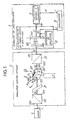
- the electro-optical spectrum analyzer comprises a laser source 1, an electro-optical modulator 2, and a spectroscopy device 3.
- the laser source 1 is of the monochromatic type with continuous emission and with very small line width.
- the laser source 1 is for example made up of a gas laser source of the Helium-Neon (He-Ne) type, frequency stabilized and emitting a light wave L of wavelength 0, frequency 0 and very small width of skate.
- He-Ne Helium-Neon
- the electro-optical modulator 2 is a POCKELS cell comprising a polarizer 20, a compensator 21, a crystal 22 having an electro-optical property, and a polarizer-analyzer 23.
- the polarizer 20 is for example made up of a GLAN or NICOLL prism. It receives the light wave L supplied by the laser source 1 at a first face 200 and delivers a light wave rectilinearly polarized L p by a second face 201. The light wave L p is applied through the compensator 21 to a first face 220 of the crystal 22.
- the electro-optical crystal 22 is for example made up of a crystal of ADP ((NH4) H2PO4) of parallelepiped shape.
- the crystal 22 comprises perpendicular crystallographic axes x and z to which correspond respectively extraordinary refractive indices n e and ordinary n o .
- the first face 220 of the crystal 22 is parallel to the plane defined by the crystallographic axes x and z.
- Second and third parallel faces 221 and 222 of the crystal 22 perpendicular to the first face 220 include conductive strips R between which an electrical signal to be analyzed V is applied.
- the electric signal V produces in the crystal 22 a transverse electric field E perpendicular to the direction of propagation of the light wave L p and parallel to the crystallographic axis z of the crystal 22.
- the light wave L p undergoes a phase delay ⁇ during the crossing of the crystal 22.
- the phase delay ⁇ is a function of the electrical signal V whose amplitude variations introduce into the crystal 22 modifications of its birefringence property, that is to say variations of the indices of refraction n o and n e whose difference n o- n e is substantially proportional to the electrical signal V.
- a light wave L ⁇ modulated in phase as a function of the electrical signal V is produced by crystal 22.
- the light wave L ⁇ is provided by a fourth face 223 of the crystal 22, and is applied to a first face 230 of the polarizer-analyzer 23.
- the polarizer-analyzer 23 is of the analogous type to the polarizer 20. It is oriented in a crossed manner with respect to the polarizer 20 and therefore comprises a direction ⁇ / 2 from the direction of the polarizer 20. By a second face 231 parallel to the first face 230, the polarizer 23 provides a light wave L A in rectilinear polarization crossed with respect to the light wave L p .
- the light wave L A has an amplitude modulation as a function of the electrical signal V.
- the light wave L p has a plane of polarization PL p oriented, as shown in FIG. 1, at ⁇ / 4 relative to the crystallographic axes x and z of the crystal 22, which is obtained by means of a suitable orientation of the polarizer 20 relative to the crystal 22.
- phase delay ⁇ 0 introduced by the compensator 21 being equal to ⁇ / 2
- the amplitude of the electrical signal V is generally very low compared to the value of the parameter V ⁇ of the order of a kilovolt, so that the ratio V / V ⁇ is very low and the modulator 2 operates in a zone of linearity ZL .
- the intensity IL A as a function of the signal V is expressed by the equality: IT HAS ⁇ (IL0 / 2). (1 + ⁇ .V / V ⁇ ).
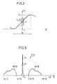
- the light wave L A modulated linearly in amplitude by the electric signal V has a frequency spectrum S ( ⁇ ) comprising a line of frequency RL at the frequency ⁇ 0 corresponding to the light wave emitted by the laser source 1 and two lateral bands BD ( ⁇ ) and BG ( ⁇ ) due to the amplitude modulation of the wave L A and corresponding to the frequency spectrum B (f) electrical signal V.
- the lateral bands BG ( ⁇ ) and BD ( ⁇ ) comprise low and high limit frequencies respectively equal to ⁇ 0-F M and ⁇ 0 + f m and ⁇ 0 + f M , where f m and f M are respectively the low and low limit frequencies high of the frequency spectrum B (f) of the signal V.
- the light wave L A therefore carries all the information relating to the electrical signal V to be analyzed and it is easy knowing the frequency spectrum of the light wave L A to deduce therefrom the frequency spectrum B (f) of the signal V .
- the spectroscopy device 3 has the function of frequency analyzing the spectrum of the light wave L A in order to determine the spectrum B (f) of the electrical signal V.
- the spectroscopy device 3 is for example made up of a scanning FABRY-PEROT interferometer 30, an optical photodiode detector 31, and an oscilloscope 32.
- the FABRY-PEROT scanning interferometer is a device well known to those skilled in the art and its operation will not be described here in detail. It essentially comprises a tunable cavity 300 and a scanning generator 301.
- the light wave L A is injected into the cavity 300 through a first semi-transparent wall 3000.
- a second semi-transparent wall 3001 of the cavity 300 is equipped with 'a piezoelectric control device and is movable in position relative to the first wall 3000.
- the movement of the wall 3001 is controlled by a low frequency scanning ramp signal BA. Under the control of the ramp signal BA, the cavity 300 is successively tuned to different frequencies of a frequency domain to be explored and delivers corresponding frequency light components CF through the second wall 3001.
- a photodiode 310 of the optical detector 31 receives the frequency light components CF supplied by the cavity 300 and delivers in response a current representative of the intensity of said components. From the current delivered by the photodiode 310, the detector 31 produces an intensity signal IF representing the intensity of the various frequency components CF in the frequency domain explored.
- the scanning ramp signal BA and the intensity signal IF are applied respectively to inputs X and Y of the oscilloscope 32 in order to display the frequency spectrum S ( ⁇ ) on the cathode-ray screen of the oscilloscope 32.
- the cavity 300 is chosen in order to present a free frequency interval between the frequency ⁇ 0 and a maximum frequency ⁇ M (Fig. 3) in which is included the lateral band BD ( ⁇ ) of the frequency spectrum S ( ⁇ ) .
- the electro-optical spectrum analyzer according to the invention can be used in order to characterize electronic components and microwave microcircuits on a semiconductor substrate.
- the microcircuit substrate consists of a crystal having an electro-optical property such as gallium arsenide (AsGa)
- AsGa gallium arsenide
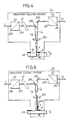
- an electro-optical modulator 2a for an in situ analysis of an electrical signal V in a microcircuit produced on an electro-optical crystalline substrate SB comprises a polarizer 20, a compensator 21, two similar mirrors 22a and 22b, a converging lens 22c, and a polarizer-analyzer 23.
- the polarizer 20, compensator 21 and polarizer-analyzer 23 are similar to those included in the modulator 2 shown in FIG. 1 and have the same functions.
- modulator 2a the crystal electro-optic 22 (Fig. 1) is deleted and the phase modulation of the polarized light wave L p is carried out directly in the electro-optical crystalline substrate SB.
- the light wave L p polarized rectilinearly and leaving the compensator 21 is oriented by the mirror 22a towards a point P in the vicinity of a conductive tape R located on an upper face FS of the substrate SB.
- the conductive tape R conveys the electrical signal to be analyzed V.
- the light wave L p is applied to the point P of the substrate SB through the converging lens 22c.
- the function of the converging lens 22c is to decrease the spatial resolution of the measurement by focusing the light wave L p on the point P which decreases on the surface and can thus be brought closer to the conductive tape R.
- the light wave L p is directed towards the point P with an angle of incidence substantially less than ⁇ / 2 and propagates in the substrate SB to a metallized lower face FI brought to a reference voltage.
- the light wave L p is retroreflected towards the upper face FS.
- the light wave leaving the substrate SB via the upper face FS is phase modulated and forms the light wave L ⁇ .
- the electric signal V produces an electric field E substantially longitudinal to the directions of propagation of the incident and reflected light waves. By electro-optical effect, the light waves propagating in the substrate SB undergo a phase delay as a function of the electrical signal V.
- the light wave L ⁇ leaving the substrate SB passes through the converging lens 22c and is directed by the mirror 22b to the first face 230 of the polarizer-analyzer 23.
- the polarizer-analyzer 23 delivers the light wave L A rectilinearly polarized and amplitude modulated by the electrical signal V.
- an electro-optical modulator 2b shown in FIG. 5, comprising a 22d electro-optical crystal measuring probe can be used.
- the probe 22d is then placed near the conductive tape R conveying the electrical signal V so that the probe 22d is crossed by lines of the electric field E produced by the signal V. It is thus possible to analyze the electric signal V without any connection between the conductive tape R and the electro-optical modulator 2b.
- the invention can give rise to multiple embodiments other than those described with reference to FIGS. 1 to 5.
- the spectroscopy device 3 included in the analyzer and described with reference to FIG. 1 can be used.
- An oscilloscope representation of the spectrum of the signal to be analyzed is not always desired.
- the spectroscopy device consists for example of a spectrograph with a dispersive element delivering a recording of the spectrum on a paper support.
- the invention can take the form of a frequency meter and include, for example, a tuned MICHELSON interferometer. manually until the photodiode optical detector 31 delivers a maximum response indicating that the interferometer is tuned to the fundamental frequency. A reading on a graduated cursor of the interferometer then indicates the desired value of the fundamental frequency of the signal.
- an electro-optical spectrum analyzer according to the invention is essentially limited by the performance of the interferometer included in the spectroscopy device and by the stability and the line width of the light wave produced by the laser source. .
- a particular embodiment of a spectrum analyzer according to the invention constituted from a FABRY-PEROT interferometer and from a commercially available laser source achieves the following performances in the case of a non-contact in situ measurement: - bandwidth of a few kilohertz at 8000 GHz, - sensitivity less than 1 mV, - spectral resolution substantially equal to 1 kHz, and - spatial resolution of a few micrometers.
Landscapes
- Physics & Mathematics (AREA)
- General Physics & Mathematics (AREA)
- Mathematical Physics (AREA)
- Nonlinear Science (AREA)
- Optics & Photonics (AREA)
- Spectrometry And Color Measurement (AREA)
- Measuring Instrument Details And Bridges, And Automatic Balancing Devices (AREA)
- Investigating Or Analysing Materials By Optical Means (AREA)
Applications Claiming Priority (2)
| Application Number | Priority Date | Filing Date | Title |
|---|---|---|---|
| FR8809735 | 1988-07-19 | ||
| FR8809735A FR2634560B1 (fr) | 1988-07-19 | 1988-07-19 | Systemes de mesure electro-optiques pour l'analyse frequentielle de signaux a tres large bande |
Publications (2)
| Publication Number | Publication Date |
|---|---|
| EP0357475A1 true EP0357475A1 (de) | 1990-03-07 |
| EP0357475B1 EP0357475B1 (de) | 1994-04-20 |
Family
ID=9368541
Family Applications (1)
| Application Number | Title | Priority Date | Filing Date |
|---|---|---|---|
| EP89402016A Expired - Lifetime EP0357475B1 (de) | 1988-07-19 | 1989-07-13 | Elektro-optisches Messverfahren für die Frequenzanalyse von Signalen hoher Bandbreite |
Country Status (6)
| Country | Link |
|---|---|
| US (1) | US5041778A (de) |
| EP (1) | EP0357475B1 (de) |
| JP (1) | JPH0247562A (de) |
| CA (1) | CA1320250C (de) |
| DE (1) | DE68914753T2 (de) |
| FR (1) | FR2634560B1 (de) |
Cited By (2)
| Publication number | Priority date | Publication date | Assignee | Title |
|---|---|---|---|---|
| US5041779A (en) * | 1990-08-17 | 1991-08-20 | The United States Of America As Represented By The Secretary Of The Army | Nonintrusive electro-optic field sensor |
| CN100399180C (zh) * | 2006-02-17 | 2008-07-02 | 中国科学院上海光学精密机械研究所 | 幅度调制效应补偿装置 |
Families Citing this family (7)
| Publication number | Priority date | Publication date | Assignee | Title |
|---|---|---|---|---|
| FR2680248B1 (fr) * | 1991-08-09 | 1993-10-08 | Slimane Loualiche | Procede et systeme de mesure de signaux electrique a haute frequence par effet electro-optique. |
| US5365237A (en) * | 1993-05-13 | 1994-11-15 | Thermo Trex Corporation | Microwave camera |
| US5481183A (en) * | 1993-05-13 | 1996-01-02 | Johnson; Paul A. | Electro-optic spectrum analyzer |
| RU2276394C1 (ru) * | 2004-09-20 | 2006-05-10 | Олег Федорович Меньших | Устройство для обнаружения эффекта резонанса "красного смещения" электромагнитных волн в анизотропных средах |
| RU2276347C1 (ru) * | 2004-10-15 | 2006-05-10 | Олег Фёдорович Меньших | Устройство для измерения "красного смещения" плоскополяризованного когерентного излучения |
| RU2428678C1 (ru) * | 2010-04-08 | 2011-09-10 | Олег Фёдорович Меньших | Устройство для регистрации вращательного электродинамического эффекта |
| RU2561143C1 (ru) * | 2014-03-03 | 2015-08-27 | Олег Фёдорович Меньших | Мостовая схема проверки вращательного магнитодинамического эффекта |
Citations (1)
| Publication number | Priority date | Publication date | Assignee | Title |
|---|---|---|---|---|
| US4695790A (en) * | 1986-01-02 | 1987-09-22 | General Dynamics Electronics Division | RF frequency spectrum analyzer subsystem |
Family Cites Families (5)
| Publication number | Priority date | Publication date | Assignee | Title |
|---|---|---|---|---|
| NL181528C (nl) * | 1980-01-12 | 1987-09-01 | Sumitomo Electric Industries | Inrichting voor het meten van een spanning of van een elektrisch veld met gebruikmaking van licht. |
| EP0058801B1 (de) * | 1980-12-17 | 1987-02-04 | Imperial Chemical Industries Plc | Messapparat mit Verwendung optischer Interferenztechnik |
| JPS58122464A (ja) * | 1982-01-13 | 1983-07-21 | Fujitsu Ltd | スペクトルアナライザ |
| US4618819A (en) * | 1984-03-27 | 1986-10-21 | The University Of Rochester | Measurement of electrical signals with subpicosecond resolution |
| US4891580A (en) * | 1988-04-29 | 1990-01-02 | American Telephone And Telegraph Co., At&T Bell Laboratories | Electro-optic measurements of voltage waveforms on electrical conductors |
-
1988
- 1988-07-19 FR FR8809735A patent/FR2634560B1/fr not_active Expired - Lifetime
-
1989
- 1989-07-13 EP EP89402016A patent/EP0357475B1/de not_active Expired - Lifetime
- 1989-07-13 DE DE68914753T patent/DE68914753T2/de not_active Expired - Fee Related
- 1989-07-17 CA CA000605846A patent/CA1320250C/en not_active Expired - Fee Related
- 1989-07-17 US US07/380,445 patent/US5041778A/en not_active Expired - Fee Related
- 1989-07-19 JP JP1184857A patent/JPH0247562A/ja active Pending
Patent Citations (1)
| Publication number | Priority date | Publication date | Assignee | Title |
|---|---|---|---|---|
| US4695790A (en) * | 1986-01-02 | 1987-09-22 | General Dynamics Electronics Division | RF frequency spectrum analyzer subsystem |
Non-Patent Citations (3)
| Title |
|---|
| IEEE JOURNAL OF QUANTUM ELECTRONICS, vol. QE-22, no. 1, 1 janvier 1986, pages 69-78, IEEE, New York, US; J.A. VALDMANIS et al.: "Subpicosecond electrooptic sampling: Principles and applications" * |
| JAPANESE JOURNAL OF APPLIED PHYSICS/PART 1: REGULAR PAPERS & SHORT NOTES, no. 6, 26 juin 1987, pages 936-940, Tokyo, JP; T. HIKITA et al.: "A versatile spectrometer by the use of a pressure-scanned fabry-perot interferometer and a piezoelectrically-scanned fabry-perot interferometer in tandem arrangement" * |
| PATENT ABSTRACTS OF JAPAN, vol. 7, no. 234 (P-230)[1379], 18 octobre 1983, page 69 P 230; & JP-A-58 122 464 (FUJITSU K.K.) 21-07-1983 * |
Cited By (2)
| Publication number | Priority date | Publication date | Assignee | Title |
|---|---|---|---|---|
| US5041779A (en) * | 1990-08-17 | 1991-08-20 | The United States Of America As Represented By The Secretary Of The Army | Nonintrusive electro-optic field sensor |
| CN100399180C (zh) * | 2006-02-17 | 2008-07-02 | 中国科学院上海光学精密机械研究所 | 幅度调制效应补偿装置 |
Also Published As
| Publication number | Publication date |
|---|---|
| FR2634560B1 (fr) | 1990-11-30 |
| EP0357475B1 (de) | 1994-04-20 |
| DE68914753T2 (de) | 1994-11-24 |
| US5041778A (en) | 1991-08-20 |
| FR2634560A1 (fr) | 1990-01-26 |
| DE68914753D1 (de) | 1994-05-26 |
| JPH0247562A (ja) | 1990-02-16 |
| CA1320250C (en) | 1993-07-13 |
Similar Documents
| Publication | Publication Date | Title |
|---|---|---|
| US4681449A (en) | High speed testing of electronic circuits by electro-optic sampling | |
| US4594511A (en) | Method and apparatus for double modulation spectroscopy | |
| JP6646519B2 (ja) | 全反射分光計測装置及び全反射分光計測方法 | |
| US20030001558A1 (en) | Method of characterizing free-space radiation using a chirped optical pulse | |
| WO2015038561A1 (en) | Cavity-enhanced frequency comb spectroscopy system employing a prism cavity | |
| Kozma et al. | Compact autocorrelator for the online measurement of tunable 10 femtosecond pulses | |
| US5256968A (en) | Measurement of high-frequency electrical signals by electro-optical effect | |
| EP0357475B1 (de) | Elektro-optisches Messverfahren für die Frequenzanalyse von Signalen hoher Bandbreite | |
| US5706084A (en) | Modulated source interferometry with combined amputude & frequency modulation | |
| EP0346386A1 (de) | Elektrooptisches netzwerkanalyse-messsystem | |
| US4910454A (en) | System for electrical signal sampling with ultrashort optical pulses | |
| JP3072814B2 (ja) | 電気光学プローブ及びその製造方法 | |
| US4982151A (en) | Voltage measuring apparatus | |
| US5737082A (en) | Method of electro-optical measurement for vector components of electric fields and an apparatus thereof | |
| JP2017211182A (ja) | 光学解析装置及び光学解析方法 | |
| WO2004027399A1 (ja) | 時間分解・非線形複素感受率測定装置 | |
| JP6652542B2 (ja) | 光学解析装置及び光学解析方法 | |
| Vickers et al. | Fabry–Pe´ rot enhancement of external electro-optic sampling | |
| EP1674878B1 (de) | Elektrooptische Sonde zur Messung elektrischer oder elektromagnetischer Felder mit einer Steuerung der Wellenlänge des Betriebspunkts | |
| JP2000171488A (ja) | 電気光学プロ―ブ | |
| CN115792402A (zh) | 一种电光探测模块、高压电脉冲信号测量装置和方法 | |
| WO2003093777A2 (fr) | Dispositif et procede de determination du 'chirp' d'un modulateur electro-optique du type mach-zehnder | |
| EP2356511B1 (de) | Durchstimmbarer optoelektronischer Frequenz-Diskriminator | |
| Cyr et al. | PMD measurements in multipath components: the single-waveplate example | |
| Struszewski et al. | All-optical vector network analyzer with 500 GHz bandwidth and 76 MHz frequency resolution |
Legal Events
| Date | Code | Title | Description |
|---|---|---|---|
| PUAI | Public reference made under article 153(3) epc to a published international application that has entered the european phase |
Free format text: ORIGINAL CODE: 0009012 |
|
| AK | Designated contracting states |
Kind code of ref document: A1 Designated state(s): DE GB |
|
| 17P | Request for examination filed |
Effective date: 19900320 |
|
| 17Q | First examination report despatched |
Effective date: 19920327 |
|
| RAP1 | Party data changed (applicant data changed or rights of an application transferred) |
Owner name: FRANCE TELECOM |
|
| GRAA | (expected) grant |
Free format text: ORIGINAL CODE: 0009210 |
|
| AK | Designated contracting states |
Kind code of ref document: B1 Designated state(s): DE GB |
|
| REF | Corresponds to: |
Ref document number: 68914753 Country of ref document: DE Date of ref document: 19940526 |
|
| GBT | Gb: translation of ep patent filed (gb section 77(6)(a)/1977) |
Effective date: 19940505 |
|
| PGFP | Annual fee paid to national office [announced via postgrant information from national office to epo] |
Ref country code: GB Payment date: 19940615 Year of fee payment: 6 |
|
| PGFP | Annual fee paid to national office [announced via postgrant information from national office to epo] |
Ref country code: DE Payment date: 19940721 Year of fee payment: 6 |
|
| PLBE | No opposition filed within time limit |
Free format text: ORIGINAL CODE: 0009261 |
|
| STAA | Information on the status of an ep patent application or granted ep patent |
Free format text: STATUS: NO OPPOSITION FILED WITHIN TIME LIMIT |
|
| 26N | No opposition filed | ||
| PG25 | Lapsed in a contracting state [announced via postgrant information from national office to epo] |
Ref country code: GB Effective date: 19950713 |
|
| GBPC | Gb: european patent ceased through non-payment of renewal fee |
Effective date: 19950713 |
|
| PG25 | Lapsed in a contracting state [announced via postgrant information from national office to epo] |
Ref country code: DE Effective date: 19960402 |