EP0357475B1 - Elektro-optisches Messverfahren für die Frequenzanalyse von Signalen hoher Bandbreite - Google Patents
Elektro-optisches Messverfahren für die Frequenzanalyse von Signalen hoher Bandbreite Download PDFInfo
- Publication number
- EP0357475B1 EP0357475B1 EP89402016A EP89402016A EP0357475B1 EP 0357475 B1 EP0357475 B1 EP 0357475B1 EP 89402016 A EP89402016 A EP 89402016A EP 89402016 A EP89402016 A EP 89402016A EP 0357475 B1 EP0357475 B1 EP 0357475B1
- Authority
- EP
- European Patent Office
- Prior art keywords
- light wave
- frequency
- electrical signal
- analyzed
- electro
- Prior art date
- Legal status (The legal status is an assumption and is not a legal conclusion. Google has not performed a legal analysis and makes no representation as to the accuracy of the status listed.)
- Expired - Lifetime
Links
- 238000004458 analytical method Methods 0.000 title claims description 8
- 239000013078 crystal Substances 0.000 claims description 27
- 238000001228 spectrum Methods 0.000 claims description 27
- 238000005259 measurement Methods 0.000 claims description 23
- 239000000758 substrate Substances 0.000 claims description 15
- 238000004611 spectroscopical analysis Methods 0.000 claims description 9
- 239000000523 sample Substances 0.000 claims description 8
- 230000005684 electric field Effects 0.000 claims description 6
- 230000004044 response Effects 0.000 claims description 6
- 239000004020 conductor Substances 0.000 claims 2
- 238000001514 detection method Methods 0.000 claims 2
- 230000001427 coherent effect Effects 0.000 claims 1
- 230000003287 optical effect Effects 0.000 description 13
- 238000005070 sampling Methods 0.000 description 11
- 238000011065 in-situ storage Methods 0.000 description 5
- 230000010287 polarization Effects 0.000 description 4
- 230000002123 temporal effect Effects 0.000 description 4
- CPBQJMYROZQQJC-UHFFFAOYSA-N helium neon Chemical compound [He].[Ne] CPBQJMYROZQQJC-UHFFFAOYSA-N 0.000 description 3
- 238000000691 measurement method Methods 0.000 description 3
- 238000000034 method Methods 0.000 description 3
- JBRZTFJDHDCESZ-UHFFFAOYSA-N AsGa Chemical compound [As]#[Ga] JBRZTFJDHDCESZ-UHFFFAOYSA-N 0.000 description 2
- PEDCQBHIVMGVHV-UHFFFAOYSA-N Glycerine Chemical compound OCC(O)CO PEDCQBHIVMGVHV-UHFFFAOYSA-N 0.000 description 2
- 230000007423 decrease Effects 0.000 description 2
- 230000003993 interaction Effects 0.000 description 2
- 230000008569 process Effects 0.000 description 2
- 230000035945 sensitivity Effects 0.000 description 2
- 229910001218 Gallium arsenide Inorganic materials 0.000 description 1
- 230000005697 Pockels effect Effects 0.000 description 1
- 230000008901 benefit Effects 0.000 description 1
- 238000005388 cross polarization Methods 0.000 description 1
- 238000010586 diagram Methods 0.000 description 1
- 238000010249 in-situ analysis Methods 0.000 description 1
- 238000012625 in-situ measurement Methods 0.000 description 1
- 238000012986 modification Methods 0.000 description 1
- 230000004048 modification Effects 0.000 description 1
- 230000005693 optoelectronics Effects 0.000 description 1
- 230000001902 propagating effect Effects 0.000 description 1
- 230000003252 repetitive effect Effects 0.000 description 1
- 239000004065 semiconductor Substances 0.000 description 1
- 230000003595 spectral effect Effects 0.000 description 1
- VLCQZHSMCYCDJL-UHFFFAOYSA-N tribenuron methyl Chemical compound COC(=O)C1=CC=CC=C1S(=O)(=O)NC(=O)N(C)C1=NC(C)=NC(OC)=N1 VLCQZHSMCYCDJL-UHFFFAOYSA-N 0.000 description 1
Images


Classifications
-
- G—PHYSICS
- G02—OPTICS
- G02F—OPTICAL DEVICES OR ARRANGEMENTS FOR THE CONTROL OF LIGHT BY MODIFICATION OF THE OPTICAL PROPERTIES OF THE MEDIA OF THE ELEMENTS INVOLVED THEREIN; NON-LINEAR OPTICS; FREQUENCY-CHANGING OF LIGHT; OPTICAL LOGIC ELEMENTS; OPTICAL ANALOGUE/DIGITAL CONVERTERS
- G02F2/00—Demodulating light; Transferring the modulation of modulated light; Frequency-changing of light
-
- G—PHYSICS
- G01—MEASURING; TESTING
- G01R—MEASURING ELECTRIC VARIABLES; MEASURING MAGNETIC VARIABLES
- G01R23/00—Arrangements for measuring frequencies; Arrangements for analysing frequency spectra
- G01R23/16—Spectrum analysis; Fourier analysis
- G01R23/17—Spectrum analysis; Fourier analysis with optical or acoustical auxiliary devices
Definitions
- the present invention relates generally to the measurement of electrical signals with a very wide frequency band. More particularly, the invention relates to the measurement of the frequency characteristics of electrical signals with a very wide frequency band by an electro-optical measurement method.
- J.A. VALDMANIS and G. MOUROU have recently developed a method for measuring the waveform of a very wide band electrical signal by electro-optical sampling. This measurement method makes it possible to reach temporal resolutions of the order of a picosecond.
- Subpicosecond Electrooptic Sampling: Principles and Applications and published in IEEE JOURNAL OF QUANTUM ELECTRONICS, VOL. QE-22, N ° 1, JANUARY 1986, J.A. VALDMANIS and G. MOUROU describe the general configuration of an electro-optical sampling measurement system.
- This measurement method by electro-optical sampling exploits the existence of birefringence in certain crystals having an electro-optical property.
- a rectilinearly polarized light wave meets an electric wave produced by an electric signal in a birefringent crystal, it undergoes a polarization rotation due to the interaction with the electric wave.
- the interaction between the two waves induces a phase delay in the light wave.
- the light wave observed in cross polarization then has an intensity modulated by the electrical signal and it suffices to measure the variations in intensity of the light wave with the aid of an optical detector to trace the electrical signal.
- a light wave formed by a train of pulses of very small width is used in order to sample the electrical signal.
- An electro-optical sampling measurement system is superior in time resolution to traditional measurement systems of the purely electronic type such as the sampling oscilloscope. This superiority is mainly due to the fact that the rotation of polarization of the light wave in the electro-optical crystal is an instantaneous phenomenon which does not present a measurable time constant and consequently the temporal resolution of such a system is essentially limited only by the width of the light wave sampling pulses.
- a disadvantage of these first measurement systems with electro-optical sampling lies in the fact that it is necessary to use a laser source with pulsed emission delivering light pulses of very small width, less than the picosecond. Indeed, a laser source of this type generally has a length of several meters and is therefore very bulky. In addition, it is difficult to settle and is relatively expensive. Another important drawback of this measurement system is that it is only possible to measure signals whose repetition frequencies are integer multiples of the repetition frequency of the light pulses delivered by the laser source. In conclusion, these two drawbacks lead to the fact that these first measurement systems with electro-optical sampling remain experimental systems which are difficult to industrialize and to market.
- the pulse laser source is replaced by a continuous source, such as a helium-neon laser
- the "slow" optical detector is replaced by an ultra-fast scanning camera.
- the camera directly receives the amplitude modulated light wave emitted by the output analyzer of the electro-optical modulator.
- the system is "related" to a standard oscilloscope, but the role of the vertical amplifier and deflection plates is replaced by the ultra-fast electro-optical modulator, and instead of the modulation of the vertical position of a beam of electrons, its intensity is modulated.
- a sinusoidal generator having a frequency (85 MHz) significantly lower than the frequency band of the electrical signal to be analyzed cuts the signal to be analyzed and synchronizes the scanning of the camera, so that the continuous laser beam is repeatedly modulated by the electrical signal to be analyzed in a periodically modulated light wave which is detected in synchronism by the camera.
- the second measurement systems periodically explore the time course of an electrical signal to be analyzed, and do not indicate characteristics of the frequency spectrum of the signal to be analyzed.
- US-A-4,695,790 describes a spectrum analyzer comprising a continuous laser source, an electro-optical modulator and several sets with optical bandpass filter and optical detector connected to the output of the electro-optical modulator through a star coupler.
- An RF electrical signal to be analyzed modulates the optical wave produced by the laser source through the electro-optical modulator.
- Filtered electrical signals produced at outputs of the optical detectors are applied to a processor which processes the filtered electrical signals in parallel to produce the spectrum of the electrical signal to be analyzed.
- the invention aims not to produce the spectrum of an electrical signal but a general representation of the characteristics of the spectrum and in particular the bandwidth and the high and low limit frequencies of this spectrum.
- the invention does not use complex electronic processing means, such as a battery of optical filter-detectors according to the aforementioned American patent, but known electrical and optical devices combined judiciously.
- An electro-optical system according to the invention has the advantage, compared to the analyzer described in the American patent, of being able to analyze electrical signals at very high frequencies because most of the signal analysis is carried out by means optical.
- the system according to the invention offers temporal performances at least equivalent to those of measurement systems with electro-optical sampling but not having their drawbacks mentioned above.
- an electro-optical system according to the invention for the frequency analysis of an electrical signal is as defined by claim 1.
- the electro-optical spectrum analyzer comprises a laser source 1, an electro-optical modulator 2, and a spectroscopy device 3.
- the laser source 1 is of the monochromatic type with continuous emission and with very small line width.
- the laser source 1 is for example constituted by a gas laser source of the Helium-Neon (He-Ne) type, frequency stabilized and emitting a light wave L of wavelength ⁇ 0, of frequency f0 and of very small width of skate.
- He-Ne Helium-Neon
- the electro-optical modulator 2 is a POCKELS cell comprising a polarizer 20, a compensator 21, a crystal 22 having an electro-optical property, and a polarizer-analyzer 23.
- the polarizer 20 is for example made up of a GLAN or NICOLL prism. It receives the light wave L supplied by the laser source 1 at a first face 200 and delivers a light wave rectilinearly polarized L p by a second face 201. The light wave L p is applied through the compensator 21 to a first face 220 of the crystal 22.
- the electro-optical crystal 22 is for example made up of a crystal of ADP ((NH4) H2PO4) of parallelepiped shape.
- the crystal 22 comprises perpendicular x and z crystallographic axes to which correspond respectively extraordinary refractive indices n e and ordinary n o .
- the first face 220 of the crystal 22 is parallel to the plane defined by the crystallographic axes x and z.
- Second and third parallel faces 221 and 222 of the crystal 22 perpendicular to the first face 220 include conductive strips R between which an electrical signal to be analyzed V is applied.
- the electric signal V produces in the crystal 22 a transverse electric field E perpendicular to the direction of propagation of the light wave L p and parallel to the crystallographic axis z of the crystal 22.
- the light wave L p undergoes a phase delay ⁇ during the crossing of the crystal 22.
- the phase delay ⁇ is a function of the electrical signal V whose amplitude variations introduce into the crystal 22 modifications of its birefringence property, that is to say variations of the indices of refraction n o and n e whose difference n o- n e is substantially proportional to the electrical signal V.
- a light wave L ⁇ modulated in phase as a function of the electrical signal V is produced by crystal 22.
- the light wave L ⁇ is provided by a fourth face 223 of the crystal 22, and is applied to a first face 230 of the polarizer-analyzer 23.
- the polarizer-analyzer 23 is of the analogous type to the polarizer 20. It is oriented in a crossed manner with respect to the polarizer 20 and therefore comprises a direction ⁇ / 2 from the direction of the polarizer 20. By a second face 231 parallel to the first face 230, the polarizer 23 supplies a light wave L A in rectilinear polarization crossed with respect to the light wave L p .
- the light wave L A has an amplitude modulation as a function of the electrical signal V.
- the light wave L p has a plane of polarization PL p oriented, as shown in FIG. 1, at ⁇ / 4 relative to the crystallographic axes x and z of the crystal 22, which is obtained by means of a suitable orientation of the polarizer 20 relative to the crystal 22.
- phase delay ⁇ 0 introduced by the compensator 21 being equal to ⁇ / 2
- the amplitude of the electrical signal V is generally very low compared to the value of the parameter V ⁇ of the order of a kilovolt, so that the ratio V / V ⁇ is very low and the modulator 2 operates in a zone of linearity ZL .
- the intensity IL A as a function of the signal V is expressed by the equality: HE AT ⁇ (IL0 / 2). (1 + ⁇ .V / V ⁇ ).
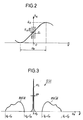
- the light wave L A linearly amplitude-modulated by the electrical signal V has a frequency spectrum S ( ⁇ ) comprising a frequency line RL at the frequency ⁇ 0 corresponding to the light wave emitted by the laser source 1 and two lateral bands BD ( ⁇ ) and BG ( ⁇ ) due to the amplitude modulation of the wave L A and corresponding to the frequency spectrum B (f) electrical signal V.
- the lateral bands BG ( ⁇ ) and BD ( ⁇ ) include low and high limit frequencies respectively equal to ⁇ 0-f M and ⁇ 0-f m , and ⁇ 0 + f m and ⁇ 0 + f M , where f m and f M are respectively the low and high limit frequencies of the frequency spectrum B (f) of the signal V.
- the light wave L A therefore carries all the information relating to the electrical signal V to be analyzed and it is easy knowing the frequency spectrum of the light wave L A to deduce therefrom the frequency spectrum B (f) of the signal V .
- the spectroscopy device 3 has the function of frequency analyzing the spectrum of the light wave L A in order to determine the spectrum B (f) of the electrical signal V.
- the spectroscopy device 3 is for example made up of a scanning FABRY-PEROT interferometer 30, an optical photodiode detector 31, and an oscilloscope 32.
- the FABRY-PEROT scanning interferometer is a device well known to those skilled in the art and its operation will not be described here in detail. It essentially comprises a tunable cavity 300 and a scanning generator 301.
- the light wave L A is injected into the cavity 300 through a first semi-transparent wall 3000.
- a second semi-transparent wall 3001 of the cavity 300 is equipped with 'a piezoelectric control device and is movable in position relative to the first wall 3000.
- the movement of the wall 3001 is controlled by a low frequency scanning ramp signal BA. Under the control of the ramp signal BA, the cavity 300 is successively tuned to different frequencies of a frequency domain to be explored and delivers corresponding frequency light components CF through the second wall 3001.
- a photodiode 310 of the optical detector 31 receives the frequency light components CF supplied by the cavity 300 and delivers in response a current representative of the intensity of said components. From the current delivered by the photodiode 310, the detector 31 produces an intensity signal IF representing the intensity of the different frequency components CF in the frequency domain explored.
- the scanning ramp signal BA and the intensity signal IF are applied respectively to inputs X and Y of the oscilloscope 32 in order to display the frequency spectrum S ( ⁇ ) on the cathode screen of the oscilloscope 32.
- the cavity 300 is chosen in order to have a free frequency interval between the frequency ⁇ 0 and a maximum frequency ⁇ M (Fig. 3) in which is included the lateral band BD ( ⁇ ) of the frequency spectrum S ( ⁇ ) .
- the electro-optical spectrum analyzer according to the invention can be used in order to characterize electronic components and microwave microcircuits on a semiconductor substrate.
- the substrate of the microcircuit consists of a crystal having an electro-optical property such as gallium arsenide (AsGa)
- AsGa gallium arsenide
- an electro-optical modulator 2a for an in situ analysis of an electrical signal V in a microcircuit produced on an electro-optical crystalline substrate SB comprises a polarizer 20, a compensator 21, two analogous mirrors 22a and 22b, a converging lens 22c, and a polarizer-analyzer 23.
- the polarizer 20, compensator 21 and polarizer-analyzer 23 are similar to those included in the modulator 2 shown in FIG. 1 and have the same functions.
- the crystal electro-optic 22 (Fig. 1) is eliminated and the phase modulation of the polarized light wave L p is carried out directly in the electro-optical crystalline substrate SB.
- the light wave L p polarized rectilinearly and leaving the compensator 21 is oriented by the mirror 22a towards a point P in the vicinity of a conductive ribbon R located on an upper face FS of the substrate SB.
- the conductive tape R conveys the electrical signal to be analyzed V.
- the light wave L p is applied to the point P of the substrate SB through the converging lens 22c.
- the function of the converging lens 22c is to decrease the spatial resolution of the measurement by focusing the light wave L p on the point P which decreases on the surface and can thus be brought closer to the conductive tape R.
- the light wave L p is directed towards the point P with an angle of incidence substantially less than ⁇ / 2 and propagates in the substrate SB to a metallized lower face FI brought to a reference voltage.
- the light wave L p is retroreflected towards the upper face FS.
- the light wave leaving the substrate SB via the upper face FS is phase modulated and forms the light wave L ⁇ .
- the electric signal V produces an electric field E substantially longitudinal to the directions of propagation of the incident and reflected light waves. By electro-optical effect, the light waves propagating in the substrate SB undergo a phase delay as a function of the electrical signal V.
- the light wave L ⁇ leaving the substrate SB passes through the converging lens 22c and is directed by the mirror 22b towards the first face 230 of the polarizer-analyzer 23.
- the polarizer-analyzer 23 delivers the light wave L A rectilinearly polarized and amplitude modulated by the electrical signal V.
- an electro-optical modulator 2b shown in FIG. 5, comprising a 22d electro-optical crystal measuring probe can be used.
- the probe 22d is then placed near the conductive tape R conveying the electrical signal V so that the probe 22d is crossed by lines of the electric field E produced by the signal V. It is thus possible to analyze the electric signal V without any connection between the conductive tape R and the electro-optical modulator 2b.
- the invention can give rise to multiple embodiments other than those described with reference to FIGS. 1 to 5.
- the spectroscopy device 3 included in the analyzer and described with reference to FIG. 1 can be used.
- An oscilloscope representation of the spectrum of the signal to be analyzed is not always desired.
- the spectroscopy device is for example made up of a spectrograph with a dispersive element delivering a recording of the spectrum on a paper support.
- the invention can take the form of a frequency meter and include for example a tuned MICHELSON interferometer manually until the photodiode optical detector 31 delivers a maximum response indicating that the interferometer is tuned to the fundamental frequency. A reading on a graduated cursor of the interferometer then indicates the desired value of the fundamental frequency of the signal.
Landscapes
- Physics & Mathematics (AREA)
- General Physics & Mathematics (AREA)
- Mathematical Physics (AREA)
- Nonlinear Science (AREA)
- Optics & Photonics (AREA)
- Spectrometry And Color Measurement (AREA)
- Measuring Instrument Details And Bridges, And Automatic Balancing Devices (AREA)
- Investigating Or Analysing Materials By Optical Means (AREA)
Claims (6)
- Elektro-optisches System zur Frequenzanalyse eines elektrischen Signals (V), in welchem vorgesehen sind
Mittel (1) zum Erzeugen und kontinuierlichen Abgeben einer ersten kohärenten monochromatischen Lichtwelle (L) konstanter Intensität,
Modulationsmittel (2) zum linearen Amplituden- oder Phasenmodulieren der ersten Lichtwelle (L) durch das zu analysierende elektrische Signal (V), um eine zweite modulierte Lichtwelle (LA) zu erzeugen, und
Spektroskopiemittel (3), die abstimmbare Frequenzmeßmittel (30) zum Empfang der zweiten Lichtquelle (LA) und, als Antwort, zur Ausgabe einer der Frequenzlichtkomponenten (CF) der zweiten Lichtwelle (LA), die eine Frequenz hat, die gleich derjenigen Frequenz ist, auf welche die abstimmbaren Frequenzmeßmittel (30) abgestimmt sind, Feststellmittel (31) zur Feststellung der Intensität der Frequenzlichtkomponenten, und Visualisationsmittel zum Sichtbarmachen (32) eines Intensitätssignals (IF) aufweisen, das von den Feststellmitteln (31) erzeugt ist und eine Intensität der einen der Frequenzlichtkomponenten (CF) repräsentiert,
dadurch gekennzeichnet, daß
die Spektroskopiemittel (3) Mittel (301) zur Erzeugung eines Frequenzabtastsignals (BA) aufweisen, welche die abstimmbaren Frequenzmeßmittel (30) sowie die Visualisationsmittel (32) nacheinander auf die verschiedenen Frequenzen des zu untersuchenden Frequenzbereichs abstimmen und ins Abtasten steuern, damit die abstimmbaren Frequenzmeßmittel (30) nacheinander die Frequenzkomponenten abgeben, um auf den ins Abtasten gesteuerten Visualisationsmitteln (32) ein Frequenzspektrum der zweiten Lichtwelle (LA) in dem zu untersuchenden Frequenzbereich anzuzeigen, um daraus die Frequenzcharakteristik (B(f)) des zu analysierenden elektrischen Signals (V) abzuleiten. - System nach Anspruch 1, dadurch gekennzeichnet, daß die Spektroskopiemittel (3) ein FABRY-PEROT Interferometer zum Abtasten aufweisen.
- System nach einem der Ansprüche 1 bis 2, dadurch gekennzeichnet, daß die Mittel (1) zum Erzeugen und Abgeben eine Laserquelle kontinuierlicher Emission umfassen, die frequenzstabilisiert ist und kleine Linienbreite hat.
- System nach einem der Ansprüche 1 bis 3, dadurch gekennzeichnet, daß die Modulationsmittel (2) einen elektro-optischen Kristall (22) aufweisen, der eine Oberfläche von Leiterstreifen (R) hat, zwischen welchen das elektrische Signal (V) aufgegeben wird, und der die erste, vorzugsweise polarisierte Lichtquelle (Lp) aufnimmt, um eine dritte Lichtquelle (Lφ) zu erzeugen, die von dem zu untersuchenden elektrischen Signal (V) phasenmoduliert ist, von welcher ausgehend ein Polarisator/Analysator (23) die zweite Lichtquelle (LA) ausgehend liefert, die von dem zu untersuchenden elektrischen Signal (V) moduliert ist.
- System nach Anspruch 4, dadurch gekennzeichnet, daß der elektro-optische Kristall durch das kristalline Substrat (2a, SB) einer Mikroschaltung oder ein zu charakterisierendes elektronisches Bauteil gebildet ist, in welchem ein elektrisches Feld (E) durch das zu untersuchende elektrische Signal (V) erzeugt ist.
- System nach einem der Ansprüche 1 bis 3, dadurch gekennzeichnet, daß die Modulationsmittel (2b) eine Meßsonde aus einem elektro-optischen Kristall (22d) umfaßt, die einem elektrischen, von dem zu untersuchenden elektrischen Signal (V) induzierten Feld (E) unterworfen ist und die erste vorzugsweise polarisierte Lichtquelle (Lp) empfängt, um eine dritte Lichtquelle (Lφ) zu erzeugen, die durch das zu untersuchende elektrische Signal (V) phasenmoduliert ist, von welcher ausgehend ein Polarisator/Analysator (23) die zweite, von dem elektrischen zu untersuchenden Signal (V) modulierte Lichtquelle (LA) liefert, wobei das elektrische Feld (E) in der Sonde (22d) durch Annähern der Sonde an einen das zu untersuchende elektrische Signal (V) führenden Leiter induziert wird.
Applications Claiming Priority (2)
| Application Number | Priority Date | Filing Date | Title |
|---|---|---|---|
| FR8809735 | 1988-07-19 | ||
| FR8809735A FR2634560B1 (fr) | 1988-07-19 | 1988-07-19 | Systemes de mesure electro-optiques pour l'analyse frequentielle de signaux a tres large bande |
Publications (2)
| Publication Number | Publication Date |
|---|---|
| EP0357475A1 EP0357475A1 (de) | 1990-03-07 |
| EP0357475B1 true EP0357475B1 (de) | 1994-04-20 |
Family
ID=9368541
Family Applications (1)
| Application Number | Title | Priority Date | Filing Date |
|---|---|---|---|
| EP89402016A Expired - Lifetime EP0357475B1 (de) | 1988-07-19 | 1989-07-13 | Elektro-optisches Messverfahren für die Frequenzanalyse von Signalen hoher Bandbreite |
Country Status (6)
| Country | Link |
|---|---|
| US (1) | US5041778A (de) |
| EP (1) | EP0357475B1 (de) |
| JP (1) | JPH0247562A (de) |
| CA (1) | CA1320250C (de) |
| DE (1) | DE68914753T2 (de) |
| FR (1) | FR2634560B1 (de) |
Families Citing this family (9)
| Publication number | Priority date | Publication date | Assignee | Title |
|---|---|---|---|---|
| US5041779A (en) * | 1990-08-17 | 1991-08-20 | The United States Of America As Represented By The Secretary Of The Army | Nonintrusive electro-optic field sensor |
| FR2680248B1 (fr) * | 1991-08-09 | 1993-10-08 | Slimane Loualiche | Procede et systeme de mesure de signaux electrique a haute frequence par effet electro-optique. |
| US5365237A (en) * | 1993-05-13 | 1994-11-15 | Thermo Trex Corporation | Microwave camera |
| US5481183A (en) * | 1993-05-13 | 1996-01-02 | Johnson; Paul A. | Electro-optic spectrum analyzer |
| RU2276394C1 (ru) * | 2004-09-20 | 2006-05-10 | Олег Федорович Меньших | Устройство для обнаружения эффекта резонанса "красного смещения" электромагнитных волн в анизотропных средах |
| RU2276347C1 (ru) * | 2004-10-15 | 2006-05-10 | Олег Фёдорович Меньших | Устройство для измерения "красного смещения" плоскополяризованного когерентного излучения |
| CN100399180C (zh) * | 2006-02-17 | 2008-07-02 | 中国科学院上海光学精密机械研究所 | 幅度调制效应补偿装置 |
| RU2428678C1 (ru) * | 2010-04-08 | 2011-09-10 | Олег Фёдорович Меньших | Устройство для регистрации вращательного электродинамического эффекта |
| RU2561143C1 (ru) * | 2014-03-03 | 2015-08-27 | Олег Фёдорович Меньших | Мостовая схема проверки вращательного магнитодинамического эффекта |
Family Cites Families (6)
| Publication number | Priority date | Publication date | Assignee | Title |
|---|---|---|---|---|
| NL181528C (nl) * | 1980-01-12 | 1987-09-01 | Sumitomo Electric Industries | Inrichting voor het meten van een spanning of van een elektrisch veld met gebruikmaking van licht. |
| EP0058801B1 (de) * | 1980-12-17 | 1987-02-04 | Imperial Chemical Industries Plc | Messapparat mit Verwendung optischer Interferenztechnik |
| JPS58122464A (ja) * | 1982-01-13 | 1983-07-21 | Fujitsu Ltd | スペクトルアナライザ |
| US4618819A (en) * | 1984-03-27 | 1986-10-21 | The University Of Rochester | Measurement of electrical signals with subpicosecond resolution |
| US4695790A (en) * | 1986-01-02 | 1987-09-22 | General Dynamics Electronics Division | RF frequency spectrum analyzer subsystem |
| US4891580A (en) * | 1988-04-29 | 1990-01-02 | American Telephone And Telegraph Co., At&T Bell Laboratories | Electro-optic measurements of voltage waveforms on electrical conductors |
-
1988
- 1988-07-19 FR FR8809735A patent/FR2634560B1/fr not_active Expired - Lifetime
-
1989
- 1989-07-13 EP EP89402016A patent/EP0357475B1/de not_active Expired - Lifetime
- 1989-07-13 DE DE68914753T patent/DE68914753T2/de not_active Expired - Fee Related
- 1989-07-17 CA CA000605846A patent/CA1320250C/en not_active Expired - Fee Related
- 1989-07-17 US US07/380,445 patent/US5041778A/en not_active Expired - Fee Related
- 1989-07-19 JP JP1184857A patent/JPH0247562A/ja active Pending
Also Published As
| Publication number | Publication date |
|---|---|
| FR2634560B1 (fr) | 1990-11-30 |
| DE68914753T2 (de) | 1994-11-24 |
| US5041778A (en) | 1991-08-20 |
| FR2634560A1 (fr) | 1990-01-26 |
| DE68914753D1 (de) | 1994-05-26 |
| EP0357475A1 (de) | 1990-03-07 |
| JPH0247562A (ja) | 1990-02-16 |
| CA1320250C (en) | 1993-07-13 |
Similar Documents
| Publication | Publication Date | Title |
|---|---|---|
| US4681449A (en) | High speed testing of electronic circuits by electro-optic sampling | |
| US5952818A (en) | Electro-optical sensing apparatus and method for characterizing free-space electromagnetic radiation | |
| US6111416A (en) | Electro-optical and magneto-optical sensing apparatus and method for characterizing free-space electromagnetic radiation | |
| EP0870180B1 (de) | Optisches bauelement zur polarisationsmodulation, und dessen verwendung in einem polarimeter oder ellipsometer | |
| US6414473B1 (en) | Electro-optic/magneto-optic measurement of electromagnetic radiation using chirped optical pulse | |
| JP6646519B2 (ja) | 全反射分光計測装置及び全反射分光計測方法 | |
| Kozma et al. | Compact autocorrelator for the online measurement of tunable 10 femtosecond pulses | |
| JP2008224452A (ja) | 全反射テラヘルツ波測定装置 | |
| WO2015038561A1 (en) | Cavity-enhanced frequency comb spectroscopy system employing a prism cavity | |
| EP0357475B1 (de) | Elektro-optisches Messverfahren für die Frequenzanalyse von Signalen hoher Bandbreite | |
| US9128059B2 (en) | Coherent anti-stokes raman spectroscopy | |
| US5256968A (en) | Measurement of high-frequency electrical signals by electro-optical effect | |
| CN114739922A (zh) | 一种多光频梳动态光谱检测系统和方法 | |
| FR2647552A1 (fr) | Systeme de mesure de signaux electriques a l'aide d'impulsions optiques ultracourtes | |
| JP3072814B2 (ja) | 電気光学プローブ及びその製造方法 | |
| US4982151A (en) | Voltage measuring apparatus | |
| JP2810976B2 (ja) | 電気信号測定方法および装置 | |
| JP3533651B1 (ja) | 時間分解・非線形複素感受率測定装置 | |
| JP6652542B2 (ja) | 光学解析装置及び光学解析方法 | |
| WO2003093777A2 (fr) | Dispositif et procede de determination du 'chirp' d'un modulateur electro-optique du type mach-zehnder | |
| JPH06273386A (ja) | 超音波の検出装置 | |
| EP2356511B1 (de) | Durchstimmbarer optoelektronischer Frequenz-Diskriminator | |
| CN115792402A (zh) | 一种电光探测模块、高压电脉冲信号测量装置和方法 | |
| Gaal et al. | Frequency counter for optical frequencies up to 40 THz | |
| Niklès et al. | Techniques for bandwidth measurements of optical guided-wave modulators |
Legal Events
| Date | Code | Title | Description |
|---|---|---|---|
| PUAI | Public reference made under article 153(3) epc to a published international application that has entered the european phase |
Free format text: ORIGINAL CODE: 0009012 |
|
| AK | Designated contracting states |
Kind code of ref document: A1 Designated state(s): DE GB |
|
| 17P | Request for examination filed |
Effective date: 19900320 |
|
| 17Q | First examination report despatched |
Effective date: 19920327 |
|
| RAP1 | Party data changed (applicant data changed or rights of an application transferred) |
Owner name: FRANCE TELECOM |
|
| GRAA | (expected) grant |
Free format text: ORIGINAL CODE: 0009210 |
|
| AK | Designated contracting states |
Kind code of ref document: B1 Designated state(s): DE GB |
|
| REF | Corresponds to: |
Ref document number: 68914753 Country of ref document: DE Date of ref document: 19940526 |
|
| GBT | Gb: translation of ep patent filed (gb section 77(6)(a)/1977) |
Effective date: 19940505 |
|
| PGFP | Annual fee paid to national office [announced via postgrant information from national office to epo] |
Ref country code: GB Payment date: 19940615 Year of fee payment: 6 |
|
| PGFP | Annual fee paid to national office [announced via postgrant information from national office to epo] |
Ref country code: DE Payment date: 19940721 Year of fee payment: 6 |
|
| PLBE | No opposition filed within time limit |
Free format text: ORIGINAL CODE: 0009261 |
|
| STAA | Information on the status of an ep patent application or granted ep patent |
Free format text: STATUS: NO OPPOSITION FILED WITHIN TIME LIMIT |
|
| 26N | No opposition filed | ||
| PG25 | Lapsed in a contracting state [announced via postgrant information from national office to epo] |
Ref country code: GB Effective date: 19950713 |
|
| GBPC | Gb: european patent ceased through non-payment of renewal fee |
Effective date: 19950713 |
|
| PG25 | Lapsed in a contracting state [announced via postgrant information from national office to epo] |
Ref country code: DE Effective date: 19960402 |