EP0358042A2 - Procédé autoaligné pour la fabrication d'une électrode de porte - Google Patents
Procédé autoaligné pour la fabrication d'une électrode de porte Download PDFInfo
- Publication number
- EP0358042A2 EP0358042A2 EP89115505A EP89115505A EP0358042A2 EP 0358042 A2 EP0358042 A2 EP 0358042A2 EP 89115505 A EP89115505 A EP 89115505A EP 89115505 A EP89115505 A EP 89115505A EP 0358042 A2 EP0358042 A2 EP 0358042A2
- Authority
- EP
- European Patent Office
- Prior art keywords
- layer
- structuring
- gate
- photoresist layer
- produced
- Prior art date
- Legal status (The legal status is an assumption and is not a legal conclusion. Google has not performed a legal analysis and makes no representation as to the accuracy of the status listed.)
- Granted
Links
Images


Classifications
-
- H—ELECTRICITY
- H10—SEMICONDUCTOR DEVICES; ELECTRIC SOLID-STATE DEVICES NOT OTHERWISE PROVIDED FOR
- H10D—INORGANIC ELECTRIC SEMICONDUCTOR DEVICES
- H10D30/00—Field-effect transistors [FET]
- H10D30/01—Manufacture or treatment
- H10D30/061—Manufacture or treatment of FETs having Schottky gates
- H10D30/0612—Manufacture or treatment of FETs having Schottky gates of lateral single-gate Schottky FETs
-
- H—ELECTRICITY
- H10—SEMICONDUCTOR DEVICES; ELECTRIC SOLID-STATE DEVICES NOT OTHERWISE PROVIDED FOR
- H10D—INORGANIC ELECTRIC SEMICONDUCTOR DEVICES
- H10D64/00—Electrodes of devices having potential barriers
- H10D64/01—Manufacture or treatment
- H10D64/012—Manufacture or treatment of electrodes comprising a Schottky barrier to a semiconductor
- H10D64/0124—Manufacture or treatment of electrodes comprising a Schottky barrier to a semiconductor to Group III-V semiconductors
- H10D64/0125—Manufacture or treatment of electrodes comprising a Schottky barrier to a semiconductor to Group III-V semiconductors characterised by the sectional shape, e.g. T or inverted T
Definitions
- the invention relates to a self-adjusting method for producing a control electrode according to the preamble of patent claim 1.
- the method is used in particular in the production of field effect transistors for analog applications which are controlled with a Schottky electrode.
- Such methods are used to manufacture field effect transistors from III / V semiconductor connections.
- at least four different substances e.g. Photoresist, silicon nitride, silicon dioxide and PMMA (polymethyl methacrylate), used for the process.
- the invention is based on the object of specifying a generic method in which the process sequence for producing the gate electrode is simplified and the transistor properties are improved.
- the process according to the invention has the advantage that the use of only two different materials for structuring the topology, the materials being able to be structured selectively, makes the process very user-friendly.
- the arrangement of the gate is determined by the special sequence of the manufacturing process and not by a critical adjustment step of the gate mask, which defines the gate position.
- Another advantage is that a small drain-source distance is produced by the self-adjusting process sequence.
- the method according to the invention begins after the production of the layer sequence for the field effect transistor and the component isolation (mesa etching or ion implantation).
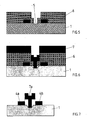
- a metal layer 4 is evaporated over the entire surface. Due to the overhang of the photoresist layer 3, the ohmic source and drain contacts 4a, 4b are formed on the component surface (FIG. 1). The metal and photoresist layers 3, 4 are removed using a lift-off process. Further process steps follow (alloying the ohmic contacts 4a, 4b) over the entire surface depositing a thin insulation layer of e.g. 0.3 ⁇ m thick SiOx (FIG.
- the desired channel thickness or position 5 of the gate is set by a wet chemical etching process in the uppermost layer of the component layer sequence 1 (gate recessing).
- a thick photoresist layer 6 of approximately 1.2 ⁇ m is then spun onto the component surface (FIG. 4). Exposing and developing the photoresist with a mask, the structure width of which is greater than the width of the dummy gate result in the in FIG. 5 shown T-shaped gate structure.
- the gate metal layer 7 applied to the photoresist layer 6 is removed by a lift-off method.
- the remaining photoresist layer 6 is removed in the 02 plasma.
- the contacts 4a, 4b, 7a are then reinforced by electroplating (FIG. 7).
- a first method variant of the self-adjusting process sequence according to the invention is based on the process shown in FIG. 2 process status shown.
- a photoresist layer 3a with a layer thickness of approximately 1.2 ⁇ m.
- a second structuring layer 8 e.g. made of germanium, evaporated with a layer thickness of approximately 10 nm.
- a thin photoresist layer 9 is spun onto the Ge layer (FIG. 8). The upper photoresist layer 9 is then exposed and developed.
- the underlying second structuring layer 8, the Ge layer is plasma-etched with CF4 + 3% 02 (FIG. 9).
- FIG. 12 shows a layer sequence applied from a thin lower photoresist layer 3b, for example made of Az 4040, a second structuring layer 8a made of eg Germanium with a layer thickness of 20 nm and an upper photoresist layer 10 made of Az 4110 at 400 rpm, for example, the layer thickness of which increases choose is that the dummy gate 2a is covered, however.
- RIE anisotropic O2 plasma etching
- the dummy gate is etched off by isotropic Cu etching, and negative photoresist edges are produced in the upper photoresist layer 10 by O2 plasma etching.
- a trapezoidal trench 11 is formed in the upper photoresist layer 10 (FIG. 14).
- the remaining dummy gate 2a is removed by plasma etching with, for example, CF4 + 3% O2 except for the component layer sequence 1.
- the gate position and the gate channel width are determined in the uppermost layer of the component layer sequence 1 by a recessing process.
- the further process steps for producing the gate electrode are, as described above and in FIGS. 6, 7 shown.
- dielectric materials can be used for the structuring layers 6, 8, which materials can be plasma-etched material-selectively compared to photoresists.
- CF4 or CHF3 or SF6 can be used as etching.
- a small drain-source distance of approximately 1 ⁇ m and a gate electrode 7a with an electrode length of approximately 0.15-0.8 ⁇ m and an electrode height of> 0.8 ⁇ m can be produced by the self-adjusting processes. It is advantageous that the ratio of height / length of the gate electrode is large with a small gate length. This advantageously reduces the lead resistance of the gate electrode (gate resistance) and the current gain of the transistor and its maximum Cutoff frequency is increased, and the minimum noise figure is also reduced.
- the gate electrode and the ohmic contacts for source and drain connection can also be produced by metal vapor deposition, which is carried out at an angle at an angle to the component surface. This advantageously reduces the parasitic source resistance.
- submicron gates down to 0.15 ⁇ m can be produced without using an electron beam recorder.
Landscapes
- Junction Field-Effect Transistors (AREA)
- Electrodes Of Semiconductors (AREA)
Applications Claiming Priority (4)
| Application Number | Priority Date | Filing Date | Title |
|---|---|---|---|
| DE3830302 | 1988-09-07 | ||
| DE3830302 | 1988-09-07 | ||
| DE3911512 | 1989-04-08 | ||
| DE3911512A DE3911512A1 (de) | 1988-09-07 | 1989-04-08 | Selbstjustierendes verfahren zur herstellung einer steuerelektrode |
Publications (3)
| Publication Number | Publication Date |
|---|---|
| EP0358042A2 true EP0358042A2 (fr) | 1990-03-14 |
| EP0358042A3 EP0358042A3 (fr) | 1991-01-09 |
| EP0358042B1 EP0358042B1 (fr) | 1995-12-06 |
Family
ID=25871918
Family Applications (1)
| Application Number | Title | Priority Date | Filing Date |
|---|---|---|---|
| EP89115505A Expired - Lifetime EP0358042B1 (fr) | 1988-09-07 | 1989-08-23 | Procédé autoaligné pour la fabrication d'une électrode de porte |
Country Status (2)
| Country | Link |
|---|---|
| EP (1) | EP0358042B1 (fr) |
| DE (2) | DE3911512A1 (fr) |
Families Citing this family (3)
| Publication number | Priority date | Publication date | Assignee | Title |
|---|---|---|---|---|
| DE3844339C2 (de) * | 1988-12-30 | 1996-11-07 | Licentia Gmbh | Verfahren zur Herstellung von Gate-Elektroden |
| DE4032411A1 (de) * | 1990-10-12 | 1992-04-16 | Daimler Benz Ag | Verfahren zur herstellung von t-gate-elektroden |
| DE10101825B4 (de) * | 2001-01-17 | 2006-12-14 | United Monolithic Semiconductors Gmbh | Verfahren zur Herstellung eines Halbleiter-Bauelements mit einer T-förmigen Kontaktelektrode |
Family Cites Families (5)
| Publication number | Priority date | Publication date | Assignee | Title |
|---|---|---|---|---|
| DE2855874A1 (de) * | 1978-12-22 | 1980-07-10 | Siemens Ag | Zahnaerztliche handstueckanordnung |
| US4341850A (en) * | 1979-07-19 | 1982-07-27 | Hughes Aircraft Company | Mask structure for forming semiconductor devices, comprising electron-sensitive resist patterns with controlled line profiles |
| JPS59229876A (ja) * | 1983-06-13 | 1984-12-24 | Toshiba Corp | シヨツトキ−ゲ−ト型電界効果トランジスタの製造方法 |
| US4616400A (en) * | 1984-12-21 | 1986-10-14 | Texas Instruments Incorporated | Process for fabricating a double recess channel field effect transistor |
| US4670090A (en) * | 1986-01-23 | 1987-06-02 | Rockwell International Corporation | Method for producing a field effect transistor |
-
1989
- 1989-04-08 DE DE3911512A patent/DE3911512A1/de not_active Ceased
- 1989-08-23 DE DE58909525T patent/DE58909525D1/de not_active Expired - Fee Related
- 1989-08-23 EP EP89115505A patent/EP0358042B1/fr not_active Expired - Lifetime
Also Published As
| Publication number | Publication date |
|---|---|
| EP0358042B1 (fr) | 1995-12-06 |
| DE3911512A1 (de) | 1990-03-22 |
| EP0358042A3 (fr) | 1991-01-09 |
| DE58909525D1 (de) | 1996-01-18 |
Similar Documents
| Publication | Publication Date | Title |
|---|---|---|
| DE69717356T2 (de) | Verfahren zur Herstellung von Heteroübergang-Bipolartransistoren mit hoher Verstärkung | |
| DE69126463T2 (de) | Verfahren zur Herstellung eines leitenden Elements | |
| DE3939319C2 (de) | Verfahren zum Herstellen eines asymmetrischen Feldeffekttransistors | |
| DE19548056C1 (de) | Verfahren zur Herstellung einer Gateelektrode für eine MOS-Struktur | |
| EP0030640B1 (fr) | Procédé pour la formation d'une électrode de porte auto-alignée pour un transistor à effet de champ V-MOS | |
| DE4138842C2 (de) | Gateelektrode und Verfahren zu deren Herstellung | |
| DE3587829T2 (de) | Verfahren zur herstellung von untereinander selbstalignierten gräben unter verwendung einer maske. | |
| DE2845460A1 (de) | Verfahren zur herstellung einer halbleitervorrichtung | |
| DE3825701A1 (de) | Verfahren zur herstellung eines bipolaren transistors | |
| DE3540422C2 (de) | Verfahren zum Herstellen integrierter Strukturen mit nicht-flüchtigen Speicherzellen, die selbst-ausgerichtete Siliciumschichten und dazugehörige Transistoren aufweisen | |
| DE69125450T2 (de) | Verfahren zur Herstellung von Feldeffekttransistoren mit einem eingefügten T-förmigen Schottky Gatter | |
| EP1354342B1 (fr) | Procede pour fabriquer un composant semi-conducteur comportant une electrode de contact en forme de t | |
| DE4446850C2 (de) | Verfahren zur Herstellung eines Transistors für eine Halbleitervorrichtung | |
| DE68918433T2 (de) | Halbleiteranordnung unter Verwendung asymmetrischer Seitewände und Verfahren zu ihrer Herstellung. | |
| EP0358042B1 (fr) | Procédé autoaligné pour la fabrication d'une électrode de porte | |
| EP0257328A1 (fr) | Procédé pour fabriquer des jonctions du type PN | |
| DE68916412T2 (de) | Halbleiteranordnung mit einem eingefügten Gate und Verfahren zur Herstellung. | |
| DE10225525A1 (de) | Verfahren zur Herstellung eines Hetero-Bipolar-Transistors und Hetero-Bipolar-Transistor | |
| DE10117741B4 (de) | Verfahren zur Herstellung eines Halbleiter-Bauelements mit T-förmigen Kontaktelektrode | |
| DE10052131C2 (de) | Verfahren zur Herstellung von Feldeffekttransistoren mit einer vollständig selbstjustierenden Technologie | |
| DE3839770A1 (de) | Verfahren zur herstellung von gate-elektroden | |
| EP1869711A2 (fr) | Production de transistors vdmos a etablissement de contact de grille optimise | |
| EP0466103A1 (fr) | Procédé de fabrication d'une métallisation par évaporation sous une direction d'incidence oblique, sur un matériau semi-conducteur | |
| DE102004031111B4 (de) | Verfahren zum Herstellen sublithografischer Gate-Strukturen eines Feldeffekttransistoren | |
| DE10330359B4 (de) | Verfahren zur Herstellung von InP-basierten Heterostruktur-Bipolartransistoren auf der Grundlage von III/V-Halbleitern |
Legal Events
| Date | Code | Title | Description |
|---|---|---|---|
| PUAI | Public reference made under article 153(3) epc to a published international application that has entered the european phase |
Free format text: ORIGINAL CODE: 0009012 |
|
| AK | Designated contracting states |
Kind code of ref document: A2 Designated state(s): DE FR GB |
|
| PUAL | Search report despatched |
Free format text: ORIGINAL CODE: 0009013 |
|
| AK | Designated contracting states |
Kind code of ref document: A3 Designated state(s): DE FR GB |
|
| 17P | Request for examination filed |
Effective date: 19910320 |
|
| 17Q | First examination report despatched |
Effective date: 19930630 |
|
| RAP1 | Party data changed (applicant data changed or rights of an application transferred) |
Owner name: TEMIC TELEFUNKEN MICROELECTRONIC GMBH Owner name: LICENTIA PATENT-VERWALTUNGS-GMBH |
|
| GRAA | (expected) grant |
Free format text: ORIGINAL CODE: 0009210 |
|
| AK | Designated contracting states |
Kind code of ref document: B1 Designated state(s): DE FR GB |
|
| REF | Corresponds to: |
Ref document number: 58909525 Country of ref document: DE Date of ref document: 19960118 |
|
| GBT | Gb: translation of ep patent filed (gb section 77(6)(a)/1977) |
Effective date: 19960221 |
|
| ET | Fr: translation filed | ||
| PGFP | Annual fee paid to national office [announced via postgrant information from national office to epo] |
Ref country code: GB Payment date: 19960717 Year of fee payment: 8 |
|
| PGFP | Annual fee paid to national office [announced via postgrant information from national office to epo] |
Ref country code: FR Payment date: 19960731 Year of fee payment: 8 |
|
| PGFP | Annual fee paid to national office [announced via postgrant information from national office to epo] |
Ref country code: DE Payment date: 19960821 Year of fee payment: 8 |
|
| PLBE | No opposition filed within time limit |
Free format text: ORIGINAL CODE: 0009261 |
|
| STAA | Information on the status of an ep patent application or granted ep patent |
Free format text: STATUS: NO OPPOSITION FILED WITHIN TIME LIMIT |
|
| 26N | No opposition filed | ||
| PG25 | Lapsed in a contracting state [announced via postgrant information from national office to epo] |
Ref country code: GB Free format text: LAPSE BECAUSE OF NON-PAYMENT OF DUE FEES Effective date: 19970823 |
|
| GBPC | Gb: european patent ceased through non-payment of renewal fee |
Effective date: 19970823 |
|
| PG25 | Lapsed in a contracting state [announced via postgrant information from national office to epo] |
Ref country code: FR Free format text: LAPSE BECAUSE OF NON-PAYMENT OF DUE FEES Effective date: 19980430 |
|
| PG25 | Lapsed in a contracting state [announced via postgrant information from national office to epo] |
Ref country code: DE Free format text: LAPSE BECAUSE OF NON-PAYMENT OF DUE FEES Effective date: 19980501 |
|
| REG | Reference to a national code |
Ref country code: FR Ref legal event code: ST |