EP0358063A2 - Träger von elektronischen Bauelementen - Google Patents
Träger von elektronischen Bauelementen Download PDFInfo
- Publication number
- EP0358063A2 EP0358063A2 EP89115742A EP89115742A EP0358063A2 EP 0358063 A2 EP0358063 A2 EP 0358063A2 EP 89115742 A EP89115742 A EP 89115742A EP 89115742 A EP89115742 A EP 89115742A EP 0358063 A2 EP0358063 A2 EP 0358063A2
- Authority
- EP
- European Patent Office
- Prior art keywords
- electronic component
- substrate
- component carrier
- carrier according
- setting
- Prior art date
- Legal status (The legal status is an assumption and is not a legal conclusion. Google has not performed a legal analysis and makes no representation as to the accuracy of the status listed.)
- Granted
Links
Images


Classifications
-
- H—ELECTRICITY
- H05—ELECTRIC TECHNIQUES NOT OTHERWISE PROVIDED FOR
- H05K—PRINTED CIRCUITS; CASINGS OR CONSTRUCTIONAL DETAILS OF ELECTRIC APPARATUS; MANUFACTURE OF ASSEMBLAGES OF ELECTRICAL COMPONENTS
- H05K13/00—Apparatus or processes specially adapted for manufacturing or adjusting assemblages of electric components
- H05K13/003—Placing of components on belts holding the terminals
- H05K13/0038—Placing of components on belts holding the terminals placing the components in a predetermined order
-
- B—PERFORMING OPERATIONS; TRANSPORTING
- B65—CONVEYING; PACKING; STORING; HANDLING THIN OR FILAMENTARY MATERIAL
- B65D—CONTAINERS FOR STORAGE OR TRANSPORT OF ARTICLES OR MATERIALS, e.g. BAGS, BARRELS, BOTTLES, BOXES, CANS, CARTONS, CRATES, DRUMS, JARS, TANKS, HOPPERS, FORWARDING CONTAINERS; ACCESSORIES, CLOSURES, OR FITTINGS THEREFOR; PACKAGING ELEMENTS; PACKAGES
- B65D73/00—Packages comprising articles attached to cards, sheets or webs
- B65D73/02—Articles, e.g. small electrical components, attached to webs
Definitions
- This invention relates to an electronic component carrier for continuously transferring and feeding electronic components, such as an integrated circuit (IC) and a large-scale integrated circuit (LSI), to an applicator for applying them to circuit boards.
- electronic components such as an integrated circuit (IC) and a large-scale integrated circuit (LSI)
- One such known carrier of the tape reel type comprises a tape-like substrate having a series of feed perforations formed through one lateral edge portion of the substrate and spaced equally from one another along the length of the substrate, and an adhesive layer formed either continuously or discontinuously on one side of the substrate, so that electronic components are bonded to the adhesive layer in spaced relation to one another.
- an electronic component carrier comprising:
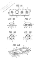
- An electronic component carrier shown in Fig. 1A comprises a tape-like substrate 1 having a suitable degree of flexibility.
- the substrate 1 has two rows of feed perforations 10 formed respectively through the opposite lateral edge portions of the substrate 1, the perforations 10 of each row being spaced at equal intervals from one another.
- the substrate 1 has at its one side a series of electronic component-mounting portions 2 disposed centrally of the width of the substrate 1 and spaced at a predetermined interval along the length of the substrate 1.
- the plane dimension of the electronic component-mounting portion 2 is substantially equal to the plane dimension of an electronic component 5 to be attached thereto.
- Push bar-insertion holes 3 are formed through the substrate 1 and are disposed at the central portions of the electronic component-mounting portions 2, respectively. The diameter of the push bar-insertion hole 3 is usually about 0.5 mm to about 10 mm.
- An adhesive layer 4 of a ring-shape is formed on the surface of each electronic component-mounting portion 2 and disposed in surrounding relation to the hole 3.
- the adhesive layer 4 is made of an adhesive of the rubber type, the acryl-type or the silicone type having suitable pressure-sensitive adhesive properties.
- the thickness of the adhesive layer 4 is usually about 1 ⁇ m to about 100 ⁇ m.
- the electronic components 5 held by the electronic component carrier of the above construction are to be supplied to an automatic applicator for applying them to circuit boards, the electronic components 5 are picked up and removed from the electronic component carrier by a suction nozzle.
- a push bar P is inserted through the hole 3 to push the electronic component 5 to facilitate the removal of the electronic component 5 from the adhesive layer 4.
- the use of the push bar P enables a smooth removal of the electronic component 5 from the adhesive layer 4.
- the substrate 1 is made of a plastic film, (preferably a film which is subjected to a electrical conductive treatment by mixing a film and a carbon powder or the like,) which has a thickness of about 0.15 mm - 1.0 mm and is made of polyethylene, polypropylene, hard polyvinyl chloride, polyester, polycarbonate and so on.
- the substrate 1 has a suitable flexibility and a self-supportability (suitable rigidity) in which a bending elastic modulus is not less than 50 kg/mm2 .
- the term "bending elastic modulus" herein used is given by a calculation method and an experiment method (which is conducted under a condition in which a temperature is 23 degree) prescribed in JIS-K6911.
- the substrate 1 is composed of the above-mentioned plastic film, so that the carrier can be easily stored by winding and the electronic component 5 is easily released from the adhesive layer 4 due to the fact that bending transformation of the substrate 1 in the upward direction can be small when the electronic component 5 is pushed up.
- Fig. 2 shows a modified electronic component carrier in which a cushioning layer 6 is interposed between the substrate 1 and the adhesive layer 4. More specifically, the cushioning layer 6 has an adhesive layer 61, and is bonded to the substrate 1 through the adhesive layer 61. With this construction, a deforming stress or an impact stress applied to the surface of the substrate 1 is absorbed and relieved by the cushioning layer 6. In addition, because of the cushioning ability of the cushioning layer 6, the adhesive layer 4 can be brought into intimate contact with an uneven surface of the electronic component 5, thereby firmly holding the electronic component 5 in a stable manner.
- the cushioning layer 6 can be made, for example, of an elastic foam of rubber and/or a synthetic resin, soft rubber, a thick non-woven fabric, or felt. The thickness of the cushioning layer 6 is about 0.05 mm to about 10 mm.
- the adhesive layer 4 be provided at the marginal portion of the electronic component-mounting portion 2, as shown in Figs. 1A and 1B. With such arrangement, the electronic component can be more positively held in position against an external impact acting in the direction of shear.
- an adhesive layer 4 may be divided into a plurality of discrete sections, so as to hold the electronic component 5 at a plurality of points.
- the adhesive layer 4 is provided in the form of a circle of dots or spots.
- an adhesive layer 4 has an uneven distribution of the adhesive strength.
- one adhesive dot 41 is omitted from the circle of adhesive dots shown in Fig. 3B.
- the adhesive layer 4 has a uniform distribution of the adhesive strength
- the releasing force is applied with an uneven distribution of stress relative to the overall adhesive layer 4, and therefore the release of the electronic component 5 from the adhesive layer can be initiated easily.
- Figs. 4A and 4B show a further modified electronic component carrier. More specifically, a substrate 1 has a number of cavity portions 11 spaced at a predetermined interval from one another along the length of the substrate 1, each cavity portion 11 being defined by a peripheral and a bottom wall. The central portion of the bottom wall of each cavity portion 11 is raised or stepped upwardly toward its opening, and an upper section of this raised portion serves as an electronic component-mounting portion 2. A push bar- insertion hole 3 is formed through the electronic component- mounting portion 2.
- the substrate 1 is formed by suitably shaping a plastics film, made, for example, of polystyrene, polypropylene, rigid polyvinyl chloride, polyester, or polycarbonate.
- the thickness of the plastics film is about 0.15 mm to about 1.0 mm. It is preferred that the plastic film be subjected to an electrically conductive treatment, for example, by adding carbon powder to the material of such plastic film.
- the substrate (1) has a suitable flexibility and a self-supportability (suitable rigidity) in which a bending elastic modulus" is not less than 50 kg/mm2.
- the two stepped portions, which perform the function of ribs and define the cavity portion 11 and the raised portion (electronic component- mounting portion) 2, respectively, are provided around the electronic component 5. Therefore, the bending strain developing in the bonding surface (the electronic component- mounting portion 2) due to an external bending force can be relieved.
- the plane dimension of the electronic component-mounting portion 2 raised as shown in Fig. 4B is substantially equal to the plane dimension of the electronic component 5 (Preferably, the difference is not more than ⁇ 20%).
- the height h of the electronic component- mounting portion 2 is 1 to 50 times greater than the thickness t . of the substrate 1.
- the plane dimension of the raised portion 2 is substantially equal to the plane dimension of the plane dimension of the electronic component 5, an right-angular corner portion is not provided between the portion 2 and the electronic component 5. Therefore, even when an external bending force is applied to the substrate 1, there is not encountered a stress concentration which would otherwise be caused by the notch effect due to such a right-angular corner portion. Also, if the height h of the electronic component- mounting portion 2 is 1 to 50 times greater than the thickness of the substrate 1, its stepped portion can perform the function of a rib which withstands an external bending force, thereby relieving the deformation of the electronic component- mounting portion 2 which would be caused by such external bending force. Therefore, the effect of such bending deformation on the interface between the electronic component- mounting portion 2 and the adhesive layer 4 is relieved, thereby preventing the portion 2 from being released from the substrate 1.
- Fig. 5 shows a further modified electronic component carrier which differs from the electronic component carrier of Figs. 4A and 4B in that a corner portion where the bottom wall 11a and the peripheral wall 11b of a cavity portion 11 are merged together is arcuately curved as at R.
- Figs. 12A and 12B show the manner in which an electronic component 5′ is removed from a conventional electronic component carrier. More specifically, when the electronic component 5′ is to be released from an adhesive layer 4′, the electronic component 5′ is held by a suction nozzle V, and is picked up. At this time, optionally, the electronic component 5′ is pushed by a push bar P.
- the suction force is applied to the bottom wall 11a′ of a cavity portion 11′ through the adhesive layer 4′.
- the material of the substrate 1′ is thin so that it can be easily shaped or formed into a predetermined configuration having the cavity portion. Therefore, a deforming stress is exerted on the bottom wall 11a′ in the direction f of the suction.
- a corner portion C where the bottom wall 11a′ and the peripheral wall 11b′ jointly constituting the cavity portion 11′ are merged together is substantially right-angular, the bottom wall 11a′ is deformed or turned about the corner portion C in the direction of release of the electronic component 5′, as shown in Fig. 12B.
- the amount of such deformation is 3 to 5 mm.
- the position of release is displaced, and therefore the release of the electronic component 5′ can not be carried out smoothly.
- the curved corner portion R absorbs and relieves the deflection stress exerted on the bottom wall 11a. Therefore, even when the electronic component 5 is attracted by a suction nozzle or the like, the bottom wall 11a is hardly deformed, and the position of release is not displaced so much, thereby achieving a smooth release of the electronic component.
- the dimension of the curved corner portion R is represented by a radius r of curvature of its outer surface.
- the ratio of the curvature radius s to the depth D of the cavity 11 is not less than 1/10, and more preferably in the range of between 1/5 and 4/5.
- W represents the distance between two points g and g (on the opposite longer side walls ) at which the curvature of the peripheral wall 11b start.
- the ratio of r/W is in the range of between 1/70 and 1/5, and more preferably in the range of between 1/35 and 1/10. If the ratio of r/D and the ratio of r/W are less than 1/10 and 1/70, respectively, the bottom wall 11a can not sufficiently relieve a deforming stress applied thereto.
- the depth D of the cavity portion is 3 to 10 mm, and the distance W is 15 to 50 mm.
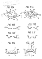
- Figs. 6A and 6B show a further modified electronic component carrier which differs from the electronic component carrier of Fig. 5 in that that portion 110 of the bottom wall 11a of the cavity portion 11 extending between the electronic- mounting portion 2 and the peripheral wall 11a of the cavity portion 11 is arcuately curved outwardly to provide an arc- shaped curved portion R.
- the curvature of this arc-shaped curved portion R can be uneven (i.e., not uniform), as shown in Figs. 6C and 6D.
- the dimension of the curved portion R is suitably determined as described above, using its shape of Fig. 6C as a reference.
- the electronic component-mounting portion 2 can be bulged downwardly to provide an annular mounting portion on which the electronic component 5 is mounted at its marginal portion through the adhesive layer 4. With this arrangement, the electronic component 5 can be stably fixed to the carrier and also can be more smoothly released from the adhesive layer 4 by the push bar.
- a polystyrene film having a thickness of 0.4 mm was formed by vacuum forming into the shape of the substrate shown in Fig. 5 to provide a substrate.
- a plurality of such substrates were prepared.
- Each of the four sides of the resultant cavity portion was 28 mm, and its depth was 5 mm.
- Each of the four sides of an electronic component- mounting portion was 15 mm, and its height was 1 mm.
- a push bar-insertion hole had a diameter of 3 mm.
- An adhesive layer having a thickness of 0.03 mm was formed on the electronic component-mounting portion of each of the substrates, and an electronic component (QFP-type LSI) was bonded to the adhesive layer. Then, the electronic component-pickup ratio was measured with respect to all the electronic component carriers thus prepared. More specifically, it was determined whether or not after the push bar was brought into contact with the electronic component, the electronic component was released from the adhesive layer when the push bar was further advanced or pushed by a distance of 5 mm.
- the electronic component-pickup ratio was calculated from the following formula:
- Comparative examples were prepared according to the same procedure except that the curved portion was not provided.
- a substrate was formed using a film having a thickness of 0.4 mm
- a substrate was formed using a film having a thickness of 0.3 mm.
- the test results of the examples and the comparative examples are shown in TABLE 1.
- TABLE 1 Size of Curvature Electronic component pickup Ratio r/D r/W Example 1 1/10 1/56 8/10
- Example 2 1/5 1/28 10/10
- Figs. 8A to 11C show further modified electronic component carriers, respectively.
- reference numeral 111 denotes a valley portion formed by a peripheral wall 11b of a cavity portion 11 and that portion 110 of a bottom wall of the cavity portion which extends between an electronic component-mounting portion 2 and the peripheral wall 11b.
- the surface of the valley portion 111 is corrugated in the direction of the periphery of the electronic component-mounting portion 2 as indicated by an arrow a (For example, the cross-section of each corrugation is rectangular). In other words, the valley portion 111 is uneven in the peripheral direction.
- the electronic component is received within the cavity portion 11 and is bonded to the electronic component-mounting portion 2 through an adhesive layer.
- the moment acts on the valley portion uniformly in its peripheral direction.
- the direction of this moment is the peripheral direction, and although the valley portion 111 is bent or deformed upwardly, the bending strain developing in the valley portion is uneven, because the surface of the valley portion 111 is uneven in its peripheral direction. Therefore, the valley portion 111 can not be so easily bent or deformed and has an increased rigidity withstanding the bending deformation.
- a sufficiently-increased vertical stress is allowed to develop between the electronic component and the adhesive layer, and therefore the electronic component can be easily released and picked up.
- the valley portion 111 has an uneven surface in the peripheral direction, it may has any shape.
- four shallow tapered surfaces 112 can be provided at four right-angular corners of a square-shaped valley portion 111, and a deeply-recessed surface 113 is formed between each two adjacent tapered surfaces 112.
- the shallow tapered surfaces 112 can be wider, that is, increased in size.
- an inclined surface 114 can be provided on each of the four corners of the square-shaped valley 111.
- the electronic components are firmly bonded adhesively to the substrate during the transfer of the electronic components, and therefore the electronic components are accurately maintained in position.
- the electronic component can be easily picked up by means of the push rod or other suitable means, thus achieving a high-speed processing of the components.
Landscapes
- Engineering & Computer Science (AREA)
- Manufacturing & Machinery (AREA)
- Microelectronics & Electronic Packaging (AREA)
- Mechanical Engineering (AREA)
- Packaging Frangible Articles (AREA)
- Packages (AREA)
Applications Claiming Priority (8)
| Application Number | Priority Date | Filing Date | Title |
|---|---|---|---|
| JP118999/88 | 1988-09-09 | ||
| JP11899988 | 1988-09-09 | ||
| JP12681688U JPH069989Y2 (ja) | 1988-09-27 | 1988-09-27 | 電子部品搬送帯 |
| JP126816/88 | 1988-09-27 | ||
| JP1989002921U JPH0734845Y2 (ja) | 1988-09-09 | 1989-01-13 | 電子部品搬送体 |
| JP2921/89 | 1989-01-13 | ||
| JP2458189U JPH0718618Y2 (ja) | 1989-03-02 | 1989-03-02 | 電子部品用搬送体 |
| JP24581/89 | 1989-03-02 |
Publications (3)
| Publication Number | Publication Date |
|---|---|
| EP0358063A2 true EP0358063A2 (de) | 1990-03-14 |
| EP0358063A3 EP0358063A3 (de) | 1991-01-30 |
| EP0358063B1 EP0358063B1 (de) | 1995-02-08 |
Family
ID=27453744
Family Applications (1)
| Application Number | Title | Priority Date | Filing Date |
|---|---|---|---|
| EP89115742A Expired - Lifetime EP0358063B1 (de) | 1988-09-09 | 1989-08-25 | Träger von elektronischen Bauelementen |
Country Status (4)
| Country | Link |
|---|---|
| US (1) | US4966281A (de) |
| EP (1) | EP0358063B1 (de) |
| DE (1) | DE68921032T2 (de) |
| MY (1) | MY104173A (de) |
Cited By (9)
| Publication number | Priority date | Publication date | Assignee | Title |
|---|---|---|---|---|
| WO1991011898A1 (en) * | 1990-01-29 | 1991-08-08 | Novapak, Inc. | Electronic component carrier |
| US5101975A (en) * | 1990-10-31 | 1992-04-07 | Novapak, Inc. | Electronic component carrier |
| US5103976A (en) * | 1990-09-25 | 1992-04-14 | R. H. Murphy Company, Inc. | Tray for integrated circuits with supporting ribs |
| WO1992014348A1 (en) * | 1991-02-12 | 1992-08-20 | Minnesota Mining And Manufacturing Company | Packaging tape |
| US5361901A (en) * | 1991-02-12 | 1994-11-08 | Minnesota Mining And Manufacturing Company | Carrier tape |
| EP0756448A3 (de) * | 1992-04-30 | 1997-03-05 | Minnesota Mining And Manufacturing Company | Trägerband mit generischen Taschen für elektronische Bauelemente |
| US5746319A (en) * | 1990-09-25 | 1998-05-05 | R.H. Murphy Co., Inc. | Tray for integrated circuits |
| US6068130A (en) * | 1999-02-05 | 2000-05-30 | Lucent Technologies Inc. | Device and method for protecting electronic component |
| EP1270438A4 (de) * | 1999-12-15 | 2009-04-29 | Denki Kagaku Kogyo Kk | Folie für geprägtes trägerband |
Families Citing this family (44)
| Publication number | Priority date | Publication date | Assignee | Title |
|---|---|---|---|---|
| GB8825154D0 (en) * | 1988-10-27 | 1988-11-30 | Reel Service Ltd | Tape for storage of electronic components |
| US5234104A (en) * | 1991-02-04 | 1993-08-10 | Illinois Tool Works Inc. | Carrier tape system |
| US5152393A (en) * | 1991-07-08 | 1992-10-06 | Advantek, Inc. | Microchip storage tape |
| US5186328A (en) * | 1991-09-23 | 1993-02-16 | Molex Incorporated | Packaging system for electrical connectors |
| US5199564A (en) * | 1992-03-13 | 1993-04-06 | Minnesota Mining And Manufacturing Company | Carrier tape for electronic through-hole components |
| US5351821A (en) * | 1992-04-30 | 1994-10-04 | Minnesota Mining And Manufacturing Company | Carrier tape with generic pockets |
| JPH07101461A (ja) * | 1993-09-30 | 1995-04-18 | Yayoi Kk | エンボスキャリアテープ |
| US5667073A (en) * | 1994-06-23 | 1997-09-16 | Okui; Tokujiro | Carrier tape for storage use of electronic components |
| JP3365058B2 (ja) * | 1994-07-07 | 2003-01-08 | 松下電器産業株式会社 | チップ部品集合体の製造方法およびチップ部品の装着方法 |
| DE4432355C2 (de) * | 1994-09-12 | 1996-11-07 | Beiersdorf Ag | Verpackung für Messer und dergleichen |
| US5518120A (en) * | 1994-12-20 | 1996-05-21 | Conductive Containers Inc. | Anti-static package for protecting sensitive electronic components from electrostatic charges |
| US5673795A (en) * | 1995-06-26 | 1997-10-07 | Minnesota Mining And Manufacturing Company | Discrete packaging system for electronic device |
| US5648136A (en) * | 1995-07-11 | 1997-07-15 | Minnesota Mining And Manufacturing Co. | Component carrier tape |
| JPH09133121A (ja) * | 1995-11-10 | 1997-05-20 | Matsushita Electric Ind Co Ltd | 部品保持体 |
| US5765692A (en) * | 1995-11-13 | 1998-06-16 | Minnesota Mining And Manufacturing Company | Carrier tape with adhesive and protective walls |
| US5664680A (en) * | 1996-04-09 | 1997-09-09 | Caritech Inc. | Pockets for microchip carriers |
| US5964353A (en) * | 1996-05-20 | 1999-10-12 | Ilinois Tool Works Inc. | Energy absorbing carrier tape |
| US6059116A (en) * | 1996-06-21 | 2000-05-09 | Thermalloy, Inc. | Heat sink packaging devices |
| KR100213874B1 (ko) * | 1996-07-29 | 1999-08-02 | 윤종용 | 전자부품이 배치된 테이프 및 이를 이용하기 위한 시스템 |
| JP3039424B2 (ja) * | 1997-02-17 | 2000-05-08 | 信越ポリマー株式会社 | エンボスキャリアテープ |
| US6016917A (en) | 1997-04-24 | 2000-01-25 | Peak International, Inc. | Component carrier having a pocket including a pedestal |
| US5833073A (en) * | 1997-06-02 | 1998-11-10 | Fluoroware, Inc. | Tacky film frame for electronic device |
| US5908114A (en) * | 1997-09-09 | 1999-06-01 | Gelpak, Llc | Tape carrier for electronic and electrical parts |
| US5878890A (en) * | 1997-09-30 | 1999-03-09 | Kaneko Denki Kabushiki Kaisha | Carrier tape |
| US6003676A (en) * | 1997-12-05 | 1999-12-21 | Tek Pak, Inc. | Product carrier and method of making same |
| US5913425A (en) * | 1997-12-08 | 1999-06-22 | Peak International, Inc. | Component carrier having anti-reflective pocket |
| US6029427A (en) * | 1999-04-05 | 2000-02-29 | Lucent Technologies, Inc. | Method and apparatus for handling semiconductor chips |
| US6398034B1 (en) * | 2000-02-29 | 2002-06-04 | National Semiconductor Corporation | Universal tape for integrated circuits |
| US6412641B1 (en) * | 2000-06-19 | 2002-07-02 | Advanced Micro Devices, Inc. | Packaging for encapsulated dice employing EMR-sensitive adhesives |
| MY126840A (en) | 2000-06-23 | 2006-10-31 | Sumitomo Bakelite Co | Electronic parts carrier tape |
| US20030209847A1 (en) * | 2002-05-10 | 2003-11-13 | Allison Claudia Leigh | Handling device comprising multiple immobilization segments |
| US20110005667A1 (en) * | 2002-05-10 | 2011-01-13 | Delphon Industries LLC | Multiple segment vacuum release handling device |
| US20030213716A1 (en) * | 2002-05-17 | 2003-11-20 | Brian Cleaver | Wafer shipping and storage container |
| US6926937B2 (en) * | 2002-09-11 | 2005-08-09 | Entegris, Inc. | Matrix tray with tacky surfaces |
| US7108899B2 (en) * | 2002-09-11 | 2006-09-19 | Entegris, Inc. | Chip tray with tacky surface |
| US7127805B2 (en) * | 2002-11-20 | 2006-10-31 | Intel Corporation | Electronic device carrier and manufacturing tape |
| JP4517856B2 (ja) * | 2004-12-27 | 2010-08-04 | Tdk株式会社 | 電子部品連 |
| JP2006199300A (ja) * | 2005-01-18 | 2006-08-03 | Matsushita Electric Ind Co Ltd | 電子部品包装帯及びその製造方法 |
| US20070074996A1 (en) * | 2005-10-05 | 2007-04-05 | Nice Travis S | Carrier tape and heat shrinking cover tape for integrated circuit devices |
| US8069636B1 (en) * | 2008-03-05 | 2011-12-06 | Charles Gutentag | Method and apparatus to facilitate retention and removal of components placed on adhesive backed carrier tape for automated handling |
| US10105927B1 (en) | 2013-03-15 | 2018-10-23 | Delphon Industries, Llc | Silicone-free thermoplastic elastomer (TPE) materials for use in carrier devices |
| US10384860B2 (en) * | 2016-07-27 | 2019-08-20 | Taiyo Yuden Co., Ltd. | Carrier tape for electronic component storage tape, electronic component storage tape, and method for manufacturing electronic component storage tape |
| WO2019118244A1 (en) | 2017-12-11 | 2019-06-20 | Delphon Industries, Llc | Carrier for reversibly immobilizing one or more objects |
| CN115604544B (zh) * | 2021-07-08 | 2025-09-09 | 荣耀终端股份有限公司 | 摄像组件及电子设备 |
Family Cites Families (9)
| Publication number | Priority date | Publication date | Assignee | Title |
|---|---|---|---|---|
| GB2040569B (en) * | 1978-12-26 | 1983-09-01 | Murata Manufacturing Co | Chip-like electronic component series and method for supplying chip-like electronic components |
| NL8005052A (nl) * | 1980-09-08 | 1982-04-01 | Philips Nv | Verpakking voor elektrische en/of elektronische componenten. |
| US4657137A (en) * | 1981-05-22 | 1987-04-14 | North American Philips Corporation | Multi-chip packaging system |
| JPS5827398A (ja) * | 1981-08-11 | 1983-02-18 | 松下電器産業株式会社 | 電子部品集合体 |
| JPS6092700A (ja) * | 1983-10-26 | 1985-05-24 | 株式会社東芝 | フラツトパツケ−ジ集積回路素子収納装置 |
| SE8403625D0 (sv) * | 1984-07-09 | 1984-07-09 | Mydata Automation Ab | Kassettmagasin for ytmonteringsmaskin |
| JPH0637489B2 (ja) * | 1985-09-21 | 1994-05-18 | 杏林製薬株式会社 | キノロンカルボン酸誘導体およびその製造方法 |
| NL8503063A (nl) * | 1985-11-08 | 1987-06-01 | Philips Nv | Bandverpakking voor elektrische en/of elektronische onderdelen. |
| GB2203676B (en) * | 1987-02-25 | 1991-03-20 | Tdk Corp | Carrier tape for electronic circuit elements and method of manufacturing an electronic circuit element series |
-
1989
- 1989-08-14 US US07/393,177 patent/US4966281A/en not_active Expired - Fee Related
- 1989-08-22 MY MYPI89001140A patent/MY104173A/en unknown
- 1989-08-25 EP EP89115742A patent/EP0358063B1/de not_active Expired - Lifetime
- 1989-08-25 DE DE68921032T patent/DE68921032T2/de not_active Expired - Fee Related
Cited By (10)
| Publication number | Priority date | Publication date | Assignee | Title |
|---|---|---|---|---|
| WO1991011898A1 (en) * | 1990-01-29 | 1991-08-08 | Novapak, Inc. | Electronic component carrier |
| US5103976A (en) * | 1990-09-25 | 1992-04-14 | R. H. Murphy Company, Inc. | Tray for integrated circuits with supporting ribs |
| US5746319A (en) * | 1990-09-25 | 1998-05-05 | R.H. Murphy Co., Inc. | Tray for integrated circuits |
| US5794784A (en) * | 1990-09-25 | 1998-08-18 | R. H. Murphy Co., Inc. | Tray for integrated circuits |
| US5101975A (en) * | 1990-10-31 | 1992-04-07 | Novapak, Inc. | Electronic component carrier |
| WO1992014348A1 (en) * | 1991-02-12 | 1992-08-20 | Minnesota Mining And Manufacturing Company | Packaging tape |
| US5361901A (en) * | 1991-02-12 | 1994-11-08 | Minnesota Mining And Manufacturing Company | Carrier tape |
| EP0756448A3 (de) * | 1992-04-30 | 1997-03-05 | Minnesota Mining And Manufacturing Company | Trägerband mit generischen Taschen für elektronische Bauelemente |
| US6068130A (en) * | 1999-02-05 | 2000-05-30 | Lucent Technologies Inc. | Device and method for protecting electronic component |
| EP1270438A4 (de) * | 1999-12-15 | 2009-04-29 | Denki Kagaku Kogyo Kk | Folie für geprägtes trägerband |
Also Published As
| Publication number | Publication date |
|---|---|
| EP0358063A3 (de) | 1991-01-30 |
| DE68921032D1 (de) | 1995-03-23 |
| EP0358063B1 (de) | 1995-02-08 |
| DE68921032T2 (de) | 1995-07-06 |
| US4966281A (en) | 1990-10-30 |
| MY104173A (en) | 1994-02-28 |
Similar Documents
| Publication | Publication Date | Title |
|---|---|---|
| EP0358063B1 (de) | Träger von elektronischen Bauelementen | |
| EP0440694B1 (de) | Gurt zur speicherung von elektronischen bauelementen | |
| US5203143A (en) | Multiple and split pressure sensitive adhesive stratums for carrier tape packaging system | |
| EP0399784B1 (de) | Nicht geschachteltes Trägerband für Bauteile | |
| US5499717A (en) | Embossed carrier tape system | |
| US5524765A (en) | Carrier tape packaging system utilizing a layer of gel for retaining small components | |
| US4702788A (en) | Method of receiving small-sized electronic parts | |
| KR100362076B1 (ko) | 테이프형상부품포장체, 부품수납용테이프, 테이프형상커버 및 부품포장장치 | |
| US5908114A (en) | Tape carrier for electronic and electrical parts | |
| US20050016898A1 (en) | Electronic package carrier tape | |
| US4654693A (en) | Electronic parts carrier with a chip-supporting top tape | |
| US5967328A (en) | Part carrier strip | |
| KR19990081983A (ko) | 부품 캐리어 테이프 | |
| KR920006163Y1 (ko) | 전자부품용 반송체 | |
| US6892886B2 (en) | Carrier tape with reinforced restraining member | |
| JPH0734845Y2 (ja) | 電子部品搬送体 | |
| KR100311820B1 (ko) | 연성기판의 엠보싱 스페이서 | |
| JPH10324388A (ja) | 電子部品の搬送帯 | |
| EP0711712B1 (de) | Band-und-Spule-Verpackungssystem für single-in-line elektronische Schaltungen | |
| JP2704202B2 (ja) | 合成樹脂製パレット | |
| JP4090615B2 (ja) | 電子部品包装容器 | |
| JPH069989Y2 (ja) | 電子部品搬送帯 | |
| JP2581686Y2 (ja) | キャリアテープ | |
| JPH0617145B2 (ja) | 電子部品搬送体 | |
| JP3907240B2 (ja) | キャリアテープ |
Legal Events
| Date | Code | Title | Description |
|---|---|---|---|
| PUAI | Public reference made under article 153(3) epc to a published international application that has entered the european phase |
Free format text: ORIGINAL CODE: 0009012 |
|
| AK | Designated contracting states |
Kind code of ref document: A2 Designated state(s): DE FR GB NL |
|
| PUAL | Search report despatched |
Free format text: ORIGINAL CODE: 0009013 |
|
| AK | Designated contracting states |
Kind code of ref document: A3 Designated state(s): DE FR GB NL |
|
| 17P | Request for examination filed |
Effective date: 19910327 |
|
| 17Q | First examination report despatched |
Effective date: 19930514 |
|
| GRAA | (expected) grant |
Free format text: ORIGINAL CODE: 0009210 |
|
| AK | Designated contracting states |
Kind code of ref document: B1 Designated state(s): DE FR GB NL |
|
| REF | Corresponds to: |
Ref document number: 68921032 Country of ref document: DE Date of ref document: 19950323 |
|
| ET | Fr: translation filed | ||
| PLBE | No opposition filed within time limit |
Free format text: ORIGINAL CODE: 0009261 |
|
| STAA | Information on the status of an ep patent application or granted ep patent |
Free format text: STATUS: NO OPPOSITION FILED WITHIN TIME LIMIT |
|
| 26N | No opposition filed | ||
| PGFP | Annual fee paid to national office [announced via postgrant information from national office to epo] |
Ref country code: FR Payment date: 19980814 Year of fee payment: 10 |
|
| PGFP | Annual fee paid to national office [announced via postgrant information from national office to epo] |
Ref country code: GB Payment date: 19980817 Year of fee payment: 10 |
|
| PGFP | Annual fee paid to national office [announced via postgrant information from national office to epo] |
Ref country code: NL Payment date: 19980827 Year of fee payment: 10 |
|
| PGFP | Annual fee paid to national office [announced via postgrant information from national office to epo] |
Ref country code: DE Payment date: 19980831 Year of fee payment: 10 |
|
| PG25 | Lapsed in a contracting state [announced via postgrant information from national office to epo] |
Ref country code: GB Free format text: LAPSE BECAUSE OF NON-PAYMENT OF DUE FEES Effective date: 19990825 |
|
| PG25 | Lapsed in a contracting state [announced via postgrant information from national office to epo] |
Ref country code: NL Free format text: LAPSE BECAUSE OF NON-PAYMENT OF DUE FEES Effective date: 20000301 |
|
| GBPC | Gb: european patent ceased through non-payment of renewal fee |
Effective date: 19990825 |
|
| PG25 | Lapsed in a contracting state [announced via postgrant information from national office to epo] |
Ref country code: FR Free format text: LAPSE BECAUSE OF NON-PAYMENT OF DUE FEES Effective date: 20000428 |
|
| NLV4 | Nl: lapsed or anulled due to non-payment of the annual fee |
Effective date: 20000301 |
|
| PG25 | Lapsed in a contracting state [announced via postgrant information from national office to epo] |
Ref country code: DE Free format text: LAPSE BECAUSE OF NON-PAYMENT OF DUE FEES Effective date: 20000601 |
|
| REG | Reference to a national code |
Ref country code: FR Ref legal event code: ST |