EP0358423B1 - Pufferspeichersubsystem für Peripheriesteuerungen und Verfahren - Google Patents
Pufferspeichersubsystem für Peripheriesteuerungen und Verfahren Download PDFInfo
- Publication number
- EP0358423B1 EP0358423B1 EP89308916A EP89308916A EP0358423B1 EP 0358423 B1 EP0358423 B1 EP 0358423B1 EP 89308916 A EP89308916 A EP 89308916A EP 89308916 A EP89308916 A EP 89308916A EP 0358423 B1 EP0358423 B1 EP 0358423B1
- Authority
- EP
- European Patent Office
- Prior art keywords
- cpu
- access
- data
- buffer
- bus
- Prior art date
- Legal status (The legal status is an assumption and is not a legal conclusion. Google has not performed a legal analysis and makes no representation as to the accuracy of the status listed.)
- Expired - Lifetime
Links
Images


Classifications
-
- G—PHYSICS
- G06—COMPUTING OR CALCULATING; COUNTING
- G06F—ELECTRIC DIGITAL DATA PROCESSING
- G06F3/00—Input arrangements for transferring data to be processed into a form capable of being handled by the computer; Output arrangements for transferring data from processing unit to output unit, e.g. interface arrangements
- G06F3/06—Digital input from, or digital output to, record carriers, e.g. RAID, emulated record carriers or networked record carriers
- G06F3/0601—Interfaces specially adapted for storage systems
-
- G—PHYSICS
- G06—COMPUTING OR CALCULATING; COUNTING
- G06F—ELECTRIC DIGITAL DATA PROCESSING
- G06F13/00—Interconnection of, or transfer of information or other signals between, memories, input/output devices or central processing units
- G06F13/10—Program control for peripheral devices
- G06F13/12—Program control for peripheral devices using hardware independent of the central processor, e.g. channel or peripheral processor
- G06F13/122—Program control for peripheral devices using hardware independent of the central processor, e.g. channel or peripheral processor where hardware performs an I/O function other than control of data transfer
-
- G—PHYSICS
- G06—COMPUTING OR CALCULATING; COUNTING
- G06F—ELECTRIC DIGITAL DATA PROCESSING
- G06F3/00—Input arrangements for transferring data to be processed into a form capable of being handled by the computer; Output arrangements for transferring data from processing unit to output unit, e.g. interface arrangements
- G06F3/06—Digital input from, or digital output to, record carriers, e.g. RAID, emulated record carriers or networked record carriers
- G06F3/0601—Interfaces specially adapted for storage systems
- G06F3/0628—Interfaces specially adapted for storage systems making use of a particular technique
- G06F3/0655—Vertical data movement, i.e. input-output transfer; data movement between one or more hosts and one or more storage devices
- G06F3/0656—Data buffering arrangements
Definitions
- the present invention relates to a buffer memory subsystem for use in data processing systems such as a buffer memory subsystem that facilitates access of data stored in a buffer memory by a peripheral controller and associated method.
- peripheral devices such as mass storage devices, printers, modems and the like often require certain control logic for proper operation.
- CPU central processing unit
- peripheral equipment became more efficient, each device could perform more activities faster, thus increasing overall data communications bus usage. This increase in bus communications resulted in increased risk of data bottleneck. Thus, more sophisticated arbitration mechanisms were required to control communications among the peripheral equipment devices and the CPU.
- peripheral controllers were developed to control peripheral devices intelligently so that CPU's could be freed for other operations.
- Each peripheral controller was provided to control individual peripheral devices on the bus. It is most efficient for a peripheral controller to control one or more devices of the same type (e.g., magnetic hard disks).
- IBM Technical Disclosure Bulletin Vol 26 No 11 p. 5956-5959 "Transparent Mode in an I/O Controller" comprises a system where the CPU accesses I/O devices via an I/O controller with fixed bus access cycle length for arbitration purposes.
- a dynamic memory as a buffer device connected to the communications bus between the peripheral devices and the peripheral controller was also proven to be very effective.
- the buffer memory allowed data from the peripheral device (e.g., disk) to be stored temporarily, pending correction, for instance. This could occur while data input to the system from a high speed data communications bus, such as a small computer system interface (SCSI), which is attached to a host processor, could be transmitted to the peripheral controller directly. In this way, communications between the peripheral device and the peripheral controller need not limit other, higher speed communications between the host processor and the rest of the peripheral subsystem.
- SCSI small computer system interface
- the data communications bus disposed between peripheral controller and buffer memory is known as a buffer bus.
- the peripheral controller has access to the buffer bus in most cases, occasionally it is the CPU that requires access to devices located on the buffer bus. In those cases, when the CPU and the peripheral controller are in contention for the buffer bus, an arbitration mechanism is required.
- arbiter was provided between the buffer bus and the peripheral controller and CPU. This arbiter consisted of external logic, requiring separate transceivers for communications with the peripheral controller and with the CPU. Recently, a desire for fewer components taking less space on printed circuit boards has made arbiters of the foregoing description inappropriate.
- a buffer memory subsystem for a peripheral controller as defined in the claims.
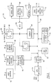
- FIGURE 1 there is shown a block diagram of the buffer memory subsystem, also known as a disk controller, in accordance with the present invention.
- the subsystem is an intelligent peripheral to a microprocessor or microcontroller, assuming the tasks of data serial format handling, data integrity and disk data management.
- a processor shown generally at reference numeral 10 in phantom includes a RAM/ROM memory 12, a central processing unit 14 and a disk interface 16.
- Processor 10 can be fabricated on one integrated circuit chip, as shown in phantom in the FIGURE, but it should be understood that processor 10 is a logical device having three separate components: memory 12, CPU 14 and disk interface 16.
- Processor 10 performs SCSI command interpretation, disk data space allocation, disk mechanical control and system interface management.
- CPU 10 For simplicity of description and to avoid confusion with a host processor described below, processor 10 will hereinafter be referred to as CPU 10.
- CPU 10 is connected to a peripheral controller 20, which is connected to the components of CPU 10 by means of a CPU bus 22.
- a host adapter 24 Also connected to peripheral controller 20 is a host adapter 24. Host adapter 24 is connected to a host processor, not shown, over a suitable high-speed data communications bus, such as an SCSI bus. Host adapter 24 is connected to peripheral controller 20 by means of an 8-bit wide buffer bus 26. This buffer bus 26 actually consists of an address portion and a data portion, not differentiated in this FIGURE. Also connected to buffer bus 26 is an external buffer memory 28 and an error processor 30.
- Peripheral controller 20 is the master of buffer memory bus 26 at all times.
- CPU 10 can access this bus 26 only when peripheral controller 20 performs necessary arbitration, as described in greater detail hereinbelow.
- Host data transfers between an SCSI device such as a processor, not shown, and external buffer memory 28 can take place on buffer bus 26 without affecting CPU data bus 22. That is, the host to peripheral controller data interface is fully autonomous and independent of CPU 10.
- a direct control/data connection allows the two devices to perform preprogrammed data transfers with minimal CPU intervention.
- a disk 32 is also provided in the system and is connected to CPU 10 by means of line 34.
- Disk 32 is a magnetic hard disk in the preferred embodiment, but may also be an optical hard disk or any other suitable form of mass storage.
- Connected between disk 32 and peripheral controller 20 are a data encoder and decoder 36 and a disk read/write logic device 38.
- FIGURE 2 there is shown a block diagram of peripheral controller 20 (FIGURE 1) in greater detail.
- a buffer bus interface controller 40 is used for arbitration of data that is intended to be transmitted over buffer bus 26.
- a control device 42 for a host processor corresponds to host adapter 24 (FIGURE 1) and is connected to buffer bus interface controller 40.
- an error processor control device 44 is also connected to buffer bus interface controller 40 and corresponds to error processor 30 (FIGURE 1).
- a buffer memory control device 46 is likewise connected to buffer bus interface controller 40 and corresponds to external buffer memory 28 (FIGURE 1). Buffer memory control device 46 is responsible for data buffering and handling. Controlling up to 4 Mbytes of dynamic buffer memory directly, the flow of data between disk 32 and host processor bus is managed via buffer memory control device 46 without CPU intervention.
- An internal sequencer data bus 48 has connected to it buffer bus interface controller 40 as well as a user register file 50, an internal sequencer RAM 52, and a sequencer unit 53, which includes a 16-bit sequencer 54 and a sequencer program ROM 56.
- Format control is a function provided in software in the preferred embodiment which can be loaded according to predetermined user disk protocol criteria. Format controller 60, however, can also be hard wired in alternate embodiments to provide a fixed format control.
- a deserializer 62 is connected to a first in first out (FIFO) register 64 which, in turn, is connected to a buffer 66 attached to buffer bus 26.
- FIFO first in first out
- Internal error detection and correction logic 68 is also provided and is connected to FIFO register 64.
- a serializer 70 is connected to FIFO 64 for converting data into a form suitable for disk 32 (FIGURE 1).
- a unit for providing disk status and control logic is shown at reference numeral 72.
- This unit 72 initiates signals prior to reading from or writing to disk 32. Initiating signals can also be generated by format controller 60.
- Connected to user register file 50 is a CPU interface 74, which is attached to CPU bus 22 (FIGURE 1).
- FIGURE 3 there is shown a detailed block diagram of the arbitration mechanism of the present invention, as embodied in buffer bus interface controller 40 (FIGURE 2) of peripheral controller 20 (FIGURE 1).
- Buffer bus interface controller 40 is disposed intermediate CPU communications bus 22, comprising an address bus 22a and a data bus 22b, and the two portions (address and data) of buffer bus 26.
- the heart of buffer bus interface controller 40 is a buffer bus arbiter unit 100.
- Arbiter 100 can be designed to be preemptible and can support single byte or multiple byte bursts depending upon the user's application requirements.
- arbiter 100 Connected to arbiter 100 are an internal sequencer access logic unit 102, a host adapter request logic unit 104, a data FIFO control logic unit 106, a refresh request logic unit 108 and a CPU access request logic unit 110.
- Each of the aforementioned units 102-110 is connected to arbiter 100 by means of request and acknowledge lines, that are used in a conventional manner.
- An interface port 112 is connected to buffer data bus 26b, the data portion of buffer bus 26. Connected to interface port 112 is also line 115, to which is connected CPU data bus 22b.
- a disk data FIFO unit 116 is connected both to data FIFO control logic unit 106 and to interface port 112 by means of line 114. Disk data FIFO unit 116 is also adapted to transmit data to disk data serializer 70 (FIGURE 2) and to receive data from disk data deserializer 62.
- Pointers 120 Connected to buffer address bus 26a is a series of pointers, shown generally at reference numeral 120.
- Pointers 120 include a sequencer pointer 120a, a CPU pointer 120b, a disk data pointer 120c and a refresh address pointer 120d.
- an address multiplexer driver 122 Connected between pointers 120 and buffer address bus 26a is an address multiplexer driver 122, which allows addresses from one pointer at a time to be loaded onto the address portion of buffer bus 26.
- a logic unit for generating control signals is also provided and identified by reference numeral 124.
- Unit 124 is adapted to generate a plurality of buffer memory read/write control signals as well as device read and device write signals and host adapter and error processor select signals.
- FIGURE 4 there is shown an address assignment diagram of peripheral controller 20 (FIGURE 1).
- Peripheral controller 20 has an address space of 256 byte-wide locations. Of these 256 locations, 128 addresses (00 through 7F) are mapped into internal registers. The remaining addresses (80 through FF) allow CPU 10 to access devices/memory on buffer bus 26.
- the internal register file can be further divided into hardware parameters, operating parameters, command parameters and status parameters. Additionally, a master control register provides overall device control.
- Locations 80 through 9F represent 32 locations shown as reference numeral 202. These locations are mapped into host adapter device 24 (FIGURE 1).
- Following reserved locations 204 having addresses A0 through BF are 32 locations from address C0 through DF, which represent locations that are mapped into error processor 30 (FIGURE 1) and are shown as reference numeral 206.
- From address E0 through FF are shown 32 locations 208 that are mapped into external buffer memory 28 (FIGURE 1).
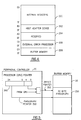
- External buffer memory 28 can be accessed by CPU 10 by means of an address pointer.
- Three data access mechanisms are provided: fixed mode, sequential mode and random mode.
- fixed mode the CPU can repeatedly access the location to which the CPU pointer points.
- sequential mode the CPU can access contiguous locations in the memory without updating the pointer. (Ther peripheral controller increments the pointer after each access.)
- random mode random access to any 32-byte section is permitted without rewriting the pointer.
- a 24-bit wide pointer 260 occupies three byte-wide locations in internal register space 200 (FIGURE 4) of peripheral controller 20. Bits 23 and 24 of pointer 260 are unused because in the preferred embodiment peripheral controller supports only a 4 Mbyte external memory 28.
- Pointer 260 can be further divided into two portions: a 17-bit paragraph pointer 250 that identifies a 32-byte area or paragraph 256 in buffer memory 28 and a 5-bit offset pointer 252 that identifies a specific byte within the 32-byte paragraph 256.
- the 5-bit offset value can be applied by CPU 10 directly.
- the buffer memory subsystem operates to allow CPU 10 to access devices and memory on the buffer bus using a flow-thru access mode.
- the total address space of the subsystem 256 locations ⁇ A[7:0]
- only the lower 128 locations 00 through 7F are mapped into internal registers.
- CPU 10 accesses a location in the upper 128 bytes (80 through FF) of address space, this request is translated into an access request for buffer bus 26.
- CPU 10 may access buffer memory 28 during the normal power up sequence in order to check memory operation, during error recovery (which occurs relatively infrequently), and when data transfer operations are to be initiated.
- the buffer bus arbiter 100 uses a fixed priority scheme under the following priorities, listed in descending order:
- buffer bus 26 two devices are supported on buffer bus 26: host adapter device 24 and error processor 30.
- CPU 10 accesses an address mapped to one of these devices 24 or 30, an access is performed on the selected device.
- the address applied to the device 24 or 30 is the same as the address on the lower five bits 258 of the CPU address lines (A[4:0]).
- the upper bits 260 are driven low.
- Addresses 80 through 9F are mapped to host adapter device 24 and addresses C0 through DF are mapped to external error processor 30.
- External buffer memory 28 can be accessed by CPU 10 at any time by executing a read or write of the register space that is mapped to buffer memory 28. That is, the buffer memory location appears as a register location of the subsystem to CPU 10. Whenever CPU 10 initiates a buffer memory access by accessing the appropriate register space, the requested access is performed. To perform the access, the arbiter 100 will have to arbitrate because buffer bus 26 may be used for another cycle at that time. The READY signal is used to lengthen the CPU cycle as required.
- buffer memory pointer 260 Part of the address of the buffer memory location to be accessed is generated by buffer memory pointer 260 loaded by CPU 10 in previous write cycles.
- Three buffer memory access modes are provided: fixed access mode, sequential access mode and paragraph random mode. They can be selected by programming a pointer control register, not shown, appropriately.
- CPU 10 accesses register location E0 again without updating the CPU pointer, the next sequential memory location is accessed and, for read operations, the value stored in that memory location is returned to CPU 10. This allows rapid sequential access to buffer memory 28 without repeated updates of the CPU pointer by CPU 10.
- This mode allows CPU 10 to set up a pointer to a 32-byte paragraph of buffer memory 28 first by writing the base address of this paragraph in the CPU pointer. CPU 10 can then access this block of memory in a fast random fashion. Addresses E0 through FF are mapped to buffer memory 28.
- CPU 10 can also access the host adapter registers specifically as follows:
- CPU 10 can also access the error processor registers specifically as follows:
Landscapes
- Engineering & Computer Science (AREA)
- Theoretical Computer Science (AREA)
- Physics & Mathematics (AREA)
- General Engineering & Computer Science (AREA)
- General Physics & Mathematics (AREA)
- Human Computer Interaction (AREA)
- Information Transfer Systems (AREA)
- Bus Control (AREA)
- Electrical Discharge Machining, Electrochemical Machining, And Combined Machining (AREA)
- Small-Scale Networks (AREA)
- Communication Control (AREA)
- Multi Processors (AREA)
- Computer And Data Communications (AREA)
Claims (21)
- Verfahren, um einer CPU zu ermöglichen, mittels einer mehrere Register aufweisenden Peripherie-Steuereinrichtung über einen Puffer-Bus auf Daten zuzugreifen, die sich in einer Speichereinrichtung befinden, mit den folgenden Schritten:(a) Initiieren eines Peripherie-Steuereinrichtungs-Zugriffszyklus an einer vorbestimmten Speicherstelle;(b) Initiieren eines CPU-Zugriffszyklus;(c) Erzeugen einer Anforderung für ein Bus-Arbiter:(d) Verlängern des CPU-Zugriffszyklus durch Negieren eines READY-Signals;(e) Ausgeben der Adresse der Speicherstelle an die Speichereinrichtung, wenn der Bus-Arbiter die Ausführung des CPU-Zugriffszyklus erlaubt;(f) Zugreifen auf die Daten an der adressierten Speicherstelle; und(g) Beenden des CPU-Zugriffszyklus durch Wirksammachen des READY-Signals.
- Verfahren nach Anspruch 1, dem die folgenden Schritte vorhergehen:(a) Programmieren eines CPU-Pointers auf die Adresse einer vorbestimmten Speicherstelle, und(b) Programmieren eines Pointersteuerregisters mit einem vorbestimmten Code.
- Verfahren nach Anspruch 2, ferner mit den folgenden Schritten:(j) Inkrementieren des CPU-Pointers derart, daß dieser auf die nächste Speicherstelle in der Speichereinrichtung verweist; und(k) Zugreifen auf die nächste Speicherstelle durch Durchführen der Schritte (c) bis (i).
- Verfahren nach Anspruch 1, bei dem der Schritt des Ausgebens der Adresse der Speicherstelle umfaßt: das Ausgeben eines ersten Sets vorbestimmter Bits der von dem CPU-Pointer spezifizierten Adresse und das Ausgeben eines zweiten Sets vorbestimmter Bits der von der CPU spezifizierten Adresse in dem aktuellen Zugriffszyklus der CPU.
- Verfahren nach einem der Ansprüche 1 bis 4, bei dem der Datenzugriff das Lesen in der Speichereinrichtung gespeicherter Daten umfaßt.
- Verfahren nach einem der Ansprüche 1 bis 4, bei dem der Datenzugriff das Speichern von Daten in der Speichereinrichtung umfaßt.
- Verfahren, um einer CPU zu ermöglichen, mittels einer mehrere Register aufweisenden Peripherie-Steuereinrichtung über einen Puffer-Bus auf Daten zuzugreifen, die sich in einem Einrichtungsregister befinden, mit den folgenden Schritten:(a) Initiieren eines Peripherie-Steuereinrichtungs-Zugriffszyklus an einer vorbestimmten Registerstelle;(b) Initiieren eines CPU-Zugriffszyklus;(c) Erzeugen einer Anforderung für einen Bus-Arbiter:(d) Verlängern des CPU-Zugriffszyklus;(e) Überführen eines durch einen Teil eines CPU-Adress-Busses repräsentierten Wertes in eine Adresse des Einrichtungsregisters, wenn der Bus-Arbiter die Ausführung des CPU-Zugriffszyklus erlaubt;(f) Zugreifen auf die Daten an der Einrichtungsregisterstelle;(g) Aktivieren eines Select-Signals und eines Zugriffssteuersignals; und(h) Beenden des CPU-Zugriffszyklus.
- Verfahren nach Anspruch 7, bei dem der CPU-Zugriffszyklus durch Negieren eines READY-Signals verlängert wird und der CPU-Zugriffszyklus durch Wirksammachen des READY-Signals beendet wird.
- Verfahren nach Anspruch 7 oder 8, bei dem Host-Adapter-Register in das Einrichtungsregister hinein abgebildet werden.
- Verfahren nach Anspruch 9, bei dem der Daten-Zugriff das Lesen in den Host-Adapter-Registern gespeicherter Daten umfaßt.
- Verfahren nach Anspruch 9, bei dem der Daten-Zugriff das Speichern von Daten in den Host-Adapter-Registern umfaßt.
- Verfahren nach Anspruch 7 oder 8, bei dem Fehlerprozessor-Register in das Einrichtungsregister hinein abgebildet werden.
- Verfahren nach Anspruch 12, bei dem der Daten-Zugriff das Lesen in den Fehlerprozessor-Registern gespeicherter Daten umfaßt.
- Verfahren nach Anspruch 12, bei dem der Daten-Zugriff das Speichern von Daten in den Fehlerprozessor-Registern umfaßt.
- Pufferspeicher-Subsystem für eine Peripherie-Steuereinrichtung, mit:(a) einem Puffer-Datenkommunikationsbus (26);(b) einer mit dem Puffer-Datenkommunikationsbus (26) verbundenen Peripherie-Steuereinrichtung (20) mit:i. mehreren Registern (200,202,204,206,208),ii. einem Bus-Arbiter (100) zum Vermitteln des über den Puffer-Datenkommunikationsbus (26) erfolgenden Zugriffs auf Daten an einer Speicherstelle einer Speichereinrichtung (28),(c) einem mit der Peripherie-Steuereinrichtung (20) verbundenen CPU-Datenkommunikationsbus (22);(d) einer von dem Puffer-Datenkommunikationsbus (26) isolierten CPU (10) mit:i. einer Einrichtung zum Initiieren eines Peripheriesteuerungs-Zugriffszyklus;ii. einer Einrichtung zum Initiieren eines CPU-Zugriffszyklus derart, daß die CPU auf eine Adresse in dem Registerraum der Peripherie-Steuereinrichtung (20) zugreifen kann;iii. einer Zugriffsanforderungs-Logik zum Erzeugen einer Anforderung für den Bus-Arbiter (100) zum Vermitteln des Zugriffs und zum anschließenden Verlängern des CPU-Zugriffszyklus durch Negieren eines READY-Signals;iv. einer Einrichtung, um eine Adresse einer Speichereinrichtungs-Speicherstelle, auf die über den Puffer-Datenkommunikationsbus (26) zugegriffen werden soll, auszugeben, wenn der Bus-Arbiter (100) den CPU-Zugriff auf diese erlaubt;v. eine Einrichtung zum Lesen/Schreiben von Daten aus der oder in die Adresse des Einrichtungsregisters, undvi. einer Einrichtung zum Beenden eines CPU-Zugriffszyklus mittels einer Einrichtung zum Wirksammachen eines READY-Signals.
- Pufferspeicher-Subsystem nach Anspruch 15, bei dem ein Prozessor-Zugriff auf in der Speichereinrichtung (28) gespeicherte Daten nur durch die Peripherie-Steuereinrichtung erlaubt ist.
- Pufferspeicher-Subsystem nach Anspruch 15, bei dem die Peripherie-Steuereinrichtung ein Steuerregister zum Identifizieren der Speichereinrichtung (28) aufweist.
- Pufferspeicher-Subsystem nach Anspruch 15, bei dem die Peripherie-Steuereinrichtung ferner eine Pointer-Steuereinrichtung zum Identifizieren vorbestimmter Speicherstellen in der Speichereinrichtung (28) aufweist.
- Pufferspeicher-Subsystem für eine Peripherie-Steuereinrichtung, mit:(a) einem Puffer-Datenkommunikationsbus (26);(b) einer mit dem Puffer-Datenkommunikationsbus (26) verbundenen Peripherie-Steuereinrichtung (20) mit:i. mehreren Registern (200,202,204,206,208),ii. einem Bus-Arbiter (100) zum Vermitteln des über den Puffer-Datenkommunikationsbus (26) erfolgenden Zugriffs auf Daten in dem Register eines Einrichtungsregisters (24,30),(c) einem mit der Peripherie-Steuereinrichtung (20) verbundenen CPU-Datenkommunikationsbus (22);(d) einer von dem Puffer-Datenkommunikationsbus (26) isolierten CPU (10) mit:i. einer Einrichtung zum Initiieren eines Peripheriesteuerungs-Zugriffszyklus;ii. einer Einrichtung zum Initiieren eines CPU-Zugriffszyklus derart, daß die CPU auf eine Adresse in dem Registerraum der Peripherie-Steuereinrichtung (20) zugreifen kann;iii. einer Zugriffsanforderungs-Logik zum Erzeugen einer Anforderung für den Bus-Arbiter (100) zum Arbitrieren des Zugriffs und zum anschließenden Verlängern des CPU-Zugriffszyklus;iv. einer Einrichtung zum Überführen eines durch einen Teil eines CPU-Adress-Busses repräsentierten Wertes an das Einrichtungsregister (24,30) auf dem Puffer-Datenkommunikationsbus (26), wenn der Bus-Arbiter (100) den CPU-Zugriff auf diesen erlaubt;v. eine Einrichtung zum Lesen/Schreiben von Daten aus der oder in die Adresse des Einrichtungsregisters,vi. einer Einrichtung zum Aktivieren eines Select-Signals und eines Zugriffssteuersignals, undvii. einer Einrichtung zum Beenden eines CPU-Zugriffszyklus.
- Pufferspeicher-Subsystem nach Anspruch 19, bei dem ein Prozessor-Zugriff auf in dem Einrichtungsregister (24,30) gespeicherte Daten nur durch die Peripherie-Steuereinrichtung erlaubt ist.
- Pufferspeicher-Subsystem nach Anspruch 19, bei dem die Peripherie-Steuereinrichtung ein Steuerregister zum Identifizieren des Einrichtungsregisters (24,30) aufweist.
Applications Claiming Priority (2)
| Application Number | Priority Date | Filing Date | Title |
|---|---|---|---|
| US07/242,743 US5239636A (en) | 1988-09-09 | 1988-09-09 | Buffer memory subsystem for peripheral controllers |
| US242743 | 1988-09-09 |
Publications (3)
| Publication Number | Publication Date |
|---|---|
| EP0358423A2 EP0358423A2 (de) | 1990-03-14 |
| EP0358423A3 EP0358423A3 (de) | 1991-03-13 |
| EP0358423B1 true EP0358423B1 (de) | 1997-05-14 |
Family
ID=22916012
Family Applications (1)
| Application Number | Title | Priority Date | Filing Date |
|---|---|---|---|
| EP89308916A Expired - Lifetime EP0358423B1 (de) | 1988-09-09 | 1989-09-04 | Pufferspeichersubsystem für Peripheriesteuerungen und Verfahren |
Country Status (7)
| Country | Link |
|---|---|
| US (1) | US5239636A (de) |
| EP (1) | EP0358423B1 (de) |
| JP (1) | JP2853809B2 (de) |
| AT (1) | ATE153150T1 (de) |
| DE (1) | DE68928040T2 (de) |
| ES (1) | ES2102979T3 (de) |
| GR (1) | GR3023419T3 (de) |
Cited By (1)
| Publication number | Priority date | Publication date | Assignee | Title |
|---|---|---|---|---|
| US6694443B1 (en) | 1992-03-27 | 2004-02-17 | National Semiconductor Corporation | System for controlling power of a microprocessor by asserting and de-asserting a control signal in response to condition associated with the microprocessor entering and exiting low power state respectively |
Families Citing this family (22)
| Publication number | Priority date | Publication date | Assignee | Title |
|---|---|---|---|---|
| US5999994A (en) * | 1991-01-31 | 1999-12-07 | Ast Research, Inc. | Dual path computer control system |
| US5829043A (en) * | 1991-04-15 | 1998-10-27 | Gilet, Deceased; Roger | Coupler circuit and its use in a card and process |
| JPH0561951A (ja) * | 1991-08-30 | 1993-03-12 | Fujitsu Ltd | イメージ処理装置 |
| US5524268A (en) * | 1992-06-26 | 1996-06-04 | Cirrus Logic, Inc. | Flexible processor-driven control of SCSI buses utilizing tags appended to data bytes to determine SCSI-protocol phases |
| US5613135A (en) * | 1992-09-17 | 1997-03-18 | Kabushiki Kaisha Toshiba | Portable computer having dedicated register group and peripheral controller bus between system bus and peripheral controller |
| TW276312B (de) * | 1992-10-20 | 1996-05-21 | Cirrlis Logic Inc | |
| US5588125A (en) * | 1993-10-20 | 1996-12-24 | Ast Research, Inc. | Method and apparatus for increasing bus bandwidth on a system bus by inhibiting interrupts while posted I/O write operations are pending |
| US5666516A (en) * | 1993-12-16 | 1997-09-09 | International Business Machines Corporation | Protected programmable memory cartridge having selective access circuitry |
| US5625800A (en) * | 1994-06-30 | 1997-04-29 | Adaptec, Inc. | SCB array external to a host adapter integrated circuit |
| US5564023A (en) * | 1994-06-30 | 1996-10-08 | Adaptec, Inc. | Method for accessing a sequencer control block by a host adapter integrated circuit |
| JPH08106733A (ja) * | 1994-10-07 | 1996-04-23 | Hitachi Ltd | 情報記憶媒体利用システム |
| WO1996032674A2 (en) * | 1995-04-13 | 1996-10-17 | Cirrus Logic, Inc. | Semiconductor memory device for mass storage block access applications |
| US5564027A (en) * | 1995-04-20 | 1996-10-08 | International Business Machines Corporation | Low latency cadence selectable interface for data transfers between busses of differing frequencies |
| US5983025A (en) * | 1995-06-07 | 1999-11-09 | International Business Machines Corporation | Computer system buffers for providing concurrency and avoid deadlock conditions between CPU accesses, local bus accesses, and memory accesses |
| US7076149B1 (en) * | 1998-07-20 | 2006-07-11 | Thomson Licensing | Digital video apparatus user interface |
| JP4233373B2 (ja) * | 2003-04-14 | 2009-03-04 | 株式会社ルネサステクノロジ | データ転送制御装置 |
| WO2009139109A1 (ja) * | 2008-05-13 | 2009-11-19 | パナソニック株式会社 | メモリ制御装置、およびこれを備えた情報処理装置 |
| US11409692B2 (en) | 2017-07-24 | 2022-08-09 | Tesla, Inc. | Vector computational unit |
| US10671349B2 (en) | 2017-07-24 | 2020-06-02 | Tesla, Inc. | Accelerated mathematical engine |
| US11157441B2 (en) | 2017-07-24 | 2021-10-26 | Tesla, Inc. | Computational array microprocessor system using non-consecutive data formatting |
| US11893393B2 (en) | 2017-07-24 | 2024-02-06 | Tesla, Inc. | Computational array microprocessor system with hardware arbiter managing memory requests |
| US11561791B2 (en) | 2018-02-01 | 2023-01-24 | Tesla, Inc. | Vector computational unit receiving data elements in parallel from a last row of a computational array |
Family Cites Families (11)
| Publication number | Priority date | Publication date | Assignee | Title |
|---|---|---|---|---|
| NL7507050A (nl) * | 1975-06-13 | 1976-12-15 | Philips Nv | Geheugensysteem. |
| US4075691A (en) * | 1975-11-06 | 1978-02-21 | Bunker Ramo Corporation | Communication control unit |
| US4236210A (en) * | 1978-10-02 | 1980-11-25 | Honeywell Information Systems Inc. | Architecture for a control store included in a data processing system |
| JPS57169865A (en) * | 1981-04-14 | 1982-10-19 | Fuji Xerox Co Ltd | Picture information storage device |
| US4543627A (en) * | 1981-12-14 | 1985-09-24 | At&T Bell Laboratories | Internal communication arrangement for a multiprocessor system |
| US4538224A (en) * | 1982-09-30 | 1985-08-27 | At&T Bell Laboratories | Direct memory access peripheral unit controller |
| US4875154A (en) * | 1983-10-13 | 1989-10-17 | Mitchell Maurice E | Microcomputer with disconnected, open, independent, bimemory architecture, allowing large interacting, interconnected multi-microcomputer parallel systems accomodating multiple levels of programmer defined heirarchy |
| US4604683A (en) * | 1984-12-10 | 1986-08-05 | Advanced Computer Communications | Communication controller using multiported random access memory |
| JPS61189386A (ja) * | 1985-02-13 | 1986-08-23 | 三菱電機株式会社 | 配管用絶縁接続装置の製造方法 |
| US4672613A (en) * | 1985-11-01 | 1987-06-09 | Cipher Data Products, Inc. | System for transferring digital data between a host device and a recording medium |
| WO1989000312A1 (en) * | 1987-07-02 | 1989-01-12 | Exabyte Corporation | Method and apparatus for data buffer management |
-
1988
- 1988-09-09 US US07/242,743 patent/US5239636A/en not_active Expired - Lifetime
-
1989
- 1989-08-29 JP JP1222791A patent/JP2853809B2/ja not_active Expired - Lifetime
- 1989-09-04 DE DE68928040T patent/DE68928040T2/de not_active Expired - Lifetime
- 1989-09-04 ES ES89308916T patent/ES2102979T3/es not_active Expired - Lifetime
- 1989-09-04 AT AT89308916T patent/ATE153150T1/de not_active IP Right Cessation
- 1989-09-04 EP EP89308916A patent/EP0358423B1/de not_active Expired - Lifetime
-
1997
- 1997-05-15 GR GR970400982T patent/GR3023419T3/el unknown
Cited By (10)
| Publication number | Priority date | Publication date | Assignee | Title |
|---|---|---|---|---|
| US6694443B1 (en) | 1992-03-27 | 2004-02-17 | National Semiconductor Corporation | System for controlling power of a microprocessor by asserting and de-asserting a control signal in response to condition associated with the microprocessor entering and exiting low power state respectively |
| US6721894B2 (en) | 1992-03-27 | 2004-04-13 | National Semiconductor Corporation | Method for controlling power of a microprocessor by asserting and de-asserting a control signal in response conditions associated with the microprocessor entering and exiting low power state respectively |
| US6910141B2 (en) | 1992-03-27 | 2005-06-21 | National Semiconductor Corporation | Pipelined data processor with signal-initiated power management control |
| US6978390B2 (en) | 1992-03-27 | 2005-12-20 | National Semiconductor Corporation | Pipelined data processor with instruction-initiated power management control |
| US7000132B2 (en) | 1992-03-27 | 2006-02-14 | National Semiconductor Corporation | Signal-initiated power management method for a pipelined data processor |
| US7062666B2 (en) | 1992-03-27 | 2006-06-13 | National Semiconductor Corporation | Signal-initiated method for suspending operation of a pipelined data processor |
| US7120810B2 (en) | 1992-03-27 | 2006-10-10 | National Semiconductor Corporation | Instruction-initiated power management method for a pipelined data processor |
| US7509512B2 (en) | 1992-03-27 | 2009-03-24 | National Semiconductor Corporation | Instruction-initiated method for suspending operation of a pipelined data processor |
| US7900076B2 (en) | 1992-03-27 | 2011-03-01 | National Semiconductor Corporation | Power management method for a pipelined computer system |
| US7900075B2 (en) | 1992-03-27 | 2011-03-01 | National Semiconductor Corporation | Pipelined computer system with power management control |
Also Published As
| Publication number | Publication date |
|---|---|
| US5239636A (en) | 1993-08-24 |
| JPH02114350A (ja) | 1990-04-26 |
| ES2102979T3 (es) | 1997-08-16 |
| ATE153150T1 (de) | 1997-05-15 |
| EP0358423A3 (de) | 1991-03-13 |
| DE68928040T2 (de) | 1998-01-08 |
| DE68928040D1 (de) | 1997-06-19 |
| JP2853809B2 (ja) | 1999-02-03 |
| EP0358423A2 (de) | 1990-03-14 |
| GR3023419T3 (en) | 1997-08-29 |
Similar Documents
| Publication | Publication Date | Title |
|---|---|---|
| EP0358423B1 (de) | Pufferspeichersubsystem für Peripheriesteuerungen und Verfahren | |
| US4937734A (en) | High speed bus with virtual memory data transfer and rerun cycle capability | |
| US6012106A (en) | Prefetch management for DMA read transactions depending upon past history of actual transfer lengths | |
| US5613162A (en) | Method and apparatus for performing efficient direct memory access data transfers | |
| US5761464A (en) | Prefetching variable length data | |
| US5301279A (en) | Apparatus for conditioning priority arbitration | |
| US5740466A (en) | Flexible processor-driven SCSI controller with buffer memory and local processor memory coupled via separate buses | |
| EP0389046B1 (de) | Intelligenter Ein-/Ausgabeprozessor und Datenverarbeitungssystem | |
| US5121487A (en) | High speed bus with virtual memory data transfer capability using virtual address/data lines | |
| CN100481043C (zh) | 用于处理输入/输出命令的方法、系统和程序 | |
| US6401149B1 (en) | Methods for context switching within a disk controller | |
| US5313582A (en) | Method and apparatus for buffering data within stations of a communication network | |
| US5787475A (en) | Controlled prefetching of data requested by a peripheral | |
| US6070204A (en) | Method and apparatus for using universal serial bus keyboard to control DOS operations | |
| US5302952A (en) | Automatic A/D converter operation with pause capability | |
| US5905911A (en) | Data transfer system which determines a size of data being transferred between a memory and an input/output device | |
| US6128674A (en) | Method of minimizing host CPU utilization in driving an adapter by residing in system memory a command/status block a soft interrupt block and a status block queue | |
| US5678064A (en) | Local bus-ISA bridge for supporting PIO and third party DMA data transfers to IDE drives | |
| US5077664A (en) | Direct memory access controller | |
| US6957280B2 (en) | Streamlining ATA device initialization | |
| EP0618537B1 (de) | Vorrichtung und Verfahren zur Verschachtelung von Zustandsinformation mit Datenübertragungen in Übertragungsadaptern | |
| EP0969384B1 (de) | Informationsverarbeitungsgerät und -verfahren, und Darstellungsmedium | |
| EP0522728B1 (de) | Verfahren zum effizienten Zugriff von Daten in einer Verknüpfungstabelle | |
| EP1188106A1 (de) | Anordnungen und verfahren für eine plattensteuerungspeicher architektur | |
| US20040162924A1 (en) | Apparatus and method for transmitting data by means of direct memory access medium |
Legal Events
| Date | Code | Title | Description |
|---|---|---|---|
| PUAI | Public reference made under article 153(3) epc to a published international application that has entered the european phase |
Free format text: ORIGINAL CODE: 0009012 |
|
| AK | Designated contracting states |
Kind code of ref document: A2 Designated state(s): AT BE CH DE ES FR GB GR IT LI LU NL SE |
|
| PUAL | Search report despatched |
Free format text: ORIGINAL CODE: 0009013 |
|
| AK | Designated contracting states |
Kind code of ref document: A3 Designated state(s): AT BE CH DE ES FR GB GR IT LI LU NL SE |
|
| 17P | Request for examination filed |
Effective date: 19910620 |
|
| 17Q | First examination report despatched |
Effective date: 19940121 |
|
| GRAG | Despatch of communication of intention to grant |
Free format text: ORIGINAL CODE: EPIDOS AGRA |
|
| GRAH | Despatch of communication of intention to grant a patent |
Free format text: ORIGINAL CODE: EPIDOS IGRA |
|
| GRAH | Despatch of communication of intention to grant a patent |
Free format text: ORIGINAL CODE: EPIDOS IGRA |
|
| GRAA | (expected) grant |
Free format text: ORIGINAL CODE: 0009210 |
|
| AK | Designated contracting states |
Kind code of ref document: B1 Designated state(s): AT BE CH DE ES FR GB GR IT LI LU NL SE |
|
| REF | Corresponds to: |
Ref document number: 153150 Country of ref document: AT Date of ref document: 19970515 Kind code of ref document: T |
|
| REG | Reference to a national code |
Ref country code: CH Ref legal event code: EP |
|
| REF | Corresponds to: |
Ref document number: 68928040 Country of ref document: DE Date of ref document: 19970619 |
|
| PGFP | Annual fee paid to national office [announced via postgrant information from national office to epo] |
Ref country code: GR Payment date: 19970725 Year of fee payment: 9 |
|
| REG | Reference to a national code |
Ref country code: GR Ref legal event code: FG4A Free format text: 3023419 |
|
| REG | Reference to a national code |
Ref country code: ES Ref legal event code: FG2A Ref document number: 2102979 Country of ref document: ES Kind code of ref document: T3 |
|
| PGFP | Annual fee paid to national office [announced via postgrant information from national office to epo] |
Ref country code: SE Payment date: 19970818 Year of fee payment: 9 |
|
| PGFP | Annual fee paid to national office [announced via postgrant information from national office to epo] |
Ref country code: AT Payment date: 19970821 Year of fee payment: 9 |
|
| ET | Fr: translation filed | ||
| REG | Reference to a national code |
Ref country code: CH Ref legal event code: NV Representative=s name: PATENTANWALTSBUREAU R. A. MASPOLI |
|
| PGFP | Annual fee paid to national office [announced via postgrant information from national office to epo] |
Ref country code: LU Payment date: 19970911 Year of fee payment: 9 |
|
| PGFP | Annual fee paid to national office [announced via postgrant information from national office to epo] |
Ref country code: BE Payment date: 19971007 Year of fee payment: 9 |
|
| PGFP | Annual fee paid to national office [announced via postgrant information from national office to epo] |
Ref country code: CH Payment date: 19971014 Year of fee payment: 9 |
|
| PLBE | No opposition filed within time limit |
Free format text: ORIGINAL CODE: 0009261 |
|
| STAA | Information on the status of an ep patent application or granted ep patent |
Free format text: STATUS: NO OPPOSITION FILED WITHIN TIME LIMIT |
|
| 26N | No opposition filed | ||
| PG25 | Lapsed in a contracting state [announced via postgrant information from national office to epo] |
Ref country code: AT Free format text: LAPSE BECAUSE OF NON-PAYMENT OF DUE FEES Effective date: 19980904 Ref country code: LU Free format text: LAPSE BECAUSE OF NON-PAYMENT OF DUE FEES Effective date: 19980904 |
|
| PG25 | Lapsed in a contracting state [announced via postgrant information from national office to epo] |
Ref country code: SE Free format text: LAPSE BECAUSE OF NON-PAYMENT OF DUE FEES Effective date: 19980905 |
|
| PG25 | Lapsed in a contracting state [announced via postgrant information from national office to epo] |
Ref country code: GR Free format text: LAPSE BECAUSE OF NON-PAYMENT OF DUE FEES Effective date: 19980930 Ref country code: BE Free format text: LAPSE BECAUSE OF NON-PAYMENT OF DUE FEES Effective date: 19980930 Ref country code: CH Free format text: LAPSE BECAUSE OF NON-PAYMENT OF DUE FEES Effective date: 19980930 Ref country code: LI Free format text: LAPSE BECAUSE OF NON-PAYMENT OF DUE FEES Effective date: 19980930 |
|
| BERE | Be: lapsed |
Owner name: ADVANCED MICRO DEVICES INC. Effective date: 19980930 |
|
| REG | Reference to a national code |
Ref country code: CH Ref legal event code: PL |
|
| EUG | Se: european patent has lapsed |
Ref document number: 89308916.9 |
|
| REG | Reference to a national code |
Ref country code: GB Ref legal event code: IF02 |
|
| PG25 | Lapsed in a contracting state [announced via postgrant information from national office to epo] |
Ref country code: IT Free format text: LAPSE BECAUSE OF NON-PAYMENT OF DUE FEES Effective date: 20050904 |
|
| PGFP | Annual fee paid to national office [announced via postgrant information from national office to epo] |
Ref country code: ES Payment date: 20080917 Year of fee payment: 20 |
|
| PGFP | Annual fee paid to national office [announced via postgrant information from national office to epo] |
Ref country code: FR Payment date: 20080904 Year of fee payment: 20 Ref country code: NL Payment date: 20080813 Year of fee payment: 20 |
|
| PGFP | Annual fee paid to national office [announced via postgrant information from national office to epo] |
Ref country code: GB Payment date: 20080808 Year of fee payment: 20 |
|
| PGFP | Annual fee paid to national office [announced via postgrant information from national office to epo] |
Ref country code: DE Payment date: 20080930 Year of fee payment: 20 |
|
| REG | Reference to a national code |
Ref country code: GB Ref legal event code: PE20 Expiry date: 20090903 |
|
| NLV7 | Nl: ceased due to reaching the maximum lifetime of a patent |
Effective date: 20090904 |
|
| REG | Reference to a national code |
Ref country code: ES Ref legal event code: FD2A Effective date: 20090905 |
|
| PG25 | Lapsed in a contracting state [announced via postgrant information from national office to epo] |
Ref country code: GB Free format text: LAPSE BECAUSE OF EXPIRATION OF PROTECTION Effective date: 20090903 Ref country code: NL Free format text: LAPSE BECAUSE OF EXPIRATION OF PROTECTION Effective date: 20090904 |
|
| REG | Reference to a national code |
Ref country code: GB Ref legal event code: 732E Free format text: REGISTERED BETWEEN 20091126 AND 20091202 |
|
| PG25 | Lapsed in a contracting state [announced via postgrant information from national office to epo] |
Ref country code: ES Free format text: LAPSE BECAUSE OF EXPIRATION OF PROTECTION Effective date: 20090905 |