EP0358425A2 - Méthode et dispositif de détection de position - Google Patents
Méthode et dispositif de détection de position Download PDFInfo
- Publication number
- EP0358425A2 EP0358425A2 EP89308921A EP89308921A EP0358425A2 EP 0358425 A2 EP0358425 A2 EP 0358425A2 EP 89308921 A EP89308921 A EP 89308921A EP 89308921 A EP89308921 A EP 89308921A EP 0358425 A2 EP0358425 A2 EP 0358425A2
- Authority
- EP
- European Patent Office
- Prior art keywords
- light
- mask
- wafer
- alignment
- sensor
- Prior art date
- Legal status (The legal status is an assumption and is not a legal conclusion. Google has not performed a legal analysis and makes no representation as to the accuracy of the status listed.)
- Withdrawn
Links
- 238000000034 method Methods 0.000 title claims description 17
- 238000001514 detection method Methods 0.000 claims abstract description 23
- 239000004065 semiconductor Substances 0.000 claims description 10
- 230000000694 effects Effects 0.000 claims description 4
- 238000004519 manufacturing process Methods 0.000 claims description 4
- 101100269850 Caenorhabditis elegans mask-1 gene Proteins 0.000 description 60
- 230000005484 gravity Effects 0.000 description 56
- 238000006073 displacement reaction Methods 0.000 description 27
- 230000003287 optical effect Effects 0.000 description 23
- 230000008859 change Effects 0.000 description 19
- 230000006870 function Effects 0.000 description 16
- 230000000875 corresponding effect Effects 0.000 description 8
- 238000012545 processing Methods 0.000 description 6
- 238000009826 distribution Methods 0.000 description 5
- 238000012937 correction Methods 0.000 description 4
- 238000002360 preparation method Methods 0.000 description 4
- 230000005540 biological transmission Effects 0.000 description 3
- 238000013461 design Methods 0.000 description 3
- 238000003384 imaging method Methods 0.000 description 3
- 238000005259 measurement Methods 0.000 description 3
- 230000035945 sensitivity Effects 0.000 description 3
- 230000000903 blocking effect Effects 0.000 description 2
- 230000001427 coherent effect Effects 0.000 description 2
- 238000000926 separation method Methods 0.000 description 2
- 239000004642 Polyimide Substances 0.000 description 1
- 238000009825 accumulation Methods 0.000 description 1
- 230000002596 correlated effect Effects 0.000 description 1
- 230000007547 defect Effects 0.000 description 1
- 238000010894 electron beam technology Methods 0.000 description 1
- 238000002474 experimental method Methods 0.000 description 1
- 238000007687 exposure technique Methods 0.000 description 1
- 238000005286 illumination Methods 0.000 description 1
- 230000010354 integration Effects 0.000 description 1
- 238000012986 modification Methods 0.000 description 1
- 230000004048 modification Effects 0.000 description 1
- 108091008695 photoreceptors Proteins 0.000 description 1
- 229920001721 polyimide Polymers 0.000 description 1
- 230000008569 process Effects 0.000 description 1
- 230000004044 response Effects 0.000 description 1
- 239000010409 thin film Substances 0.000 description 1
- 238000012546 transfer Methods 0.000 description 1
Images


Classifications
-
- G—PHYSICS
- G03—PHOTOGRAPHY; CINEMATOGRAPHY; ANALOGOUS TECHNIQUES USING WAVES OTHER THAN OPTICAL WAVES; ELECTROGRAPHY; HOLOGRAPHY
- G03F—PHOTOMECHANICAL PRODUCTION OF TEXTURED OR PATTERNED SURFACES, e.g. FOR PRINTING, FOR PROCESSING OF SEMICONDUCTOR DEVICES; MATERIALS THEREFOR; ORIGINALS THEREFOR; APPARATUS SPECIALLY ADAPTED THEREFOR
- G03F9/00—Registration or positioning of originals, masks, frames, photographic sheets or textured or patterned surfaces, e.g. automatically
- G03F9/70—Registration or positioning of originals, masks, frames, photographic sheets or textured or patterned surfaces, e.g. automatically for microlithography
- G03F9/7049—Technique, e.g. interferometric
Definitions
- This invention relates generally to a position detecting method and apparatus suitably usable, for example, in a semiconductor microcircuit device manufacturing exposure apparatus for lithographically transferring a fine electronic circuit pattern formed on the surface of a first object (original) such as a mask or reticle (hereinafter simply "mask") onto the surface of a second object (workpiece) such as a wafer, for relatively positioning or aligning the mask and the wafer.
- a first object original
- a mask or reticle hereinafter simply "mask”
- the relative alignment of a mask and a wafer is one important factor in respect to ensuring improved performance.
- alignment systems employed in recent exposure apparatuses submicron alignment accuracies or more strict accuracies are required in consideration of the demand for higher degree of integration of semiconductor devices.
- alignment patterns are provided on a mask and a wafer and, by utilizing positional information obtainable from these patterns, the mask and wafer are aligned.
- the manner of executing the alignment as an example there is a method wherein the amount of relative deviation of these alignment patterns is detected on the basis of image processing.
- Another method is proposed in U.S. Patent Nos. 4,037,969 and 4,514,858 and Japanese Laid-Open Patent Application, Laid-Open No. Sho 56-157033, wherein so-called zone plates are used as alignment patterns upon which light is projected and wherein the positions of light spots formed on a predetermined plane by lights from the illuminated zone plates are detected.
- an alignment method utilizing a zone plate is relatively insensitive to any defect of an alignment pattern and therefore assures relatively high alignment accuracies, as compared with an alignment method simply using a traditional alignment pattern.
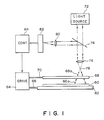
- Figure 1 is a schematic view of a known type alignment system utilizing zone plates.
- a parallel light emanating from a light source 72 passes through a half mirror 74 and is focused at a point 78 by a condensing lens 76. Thereafter, the light illuminates a mask alignment pattern 68a on a mask 68 and an alignment pattern 60a on a wafer 60 which is placed on a support table 62.
- Each of these alignment patterns 68a and 60a is provided by a reflection type zone plate and functions to form a spot of focused light on a plane perpendicular to an optical axis which contains the point 78. The amount of relative deviation of the positions of these light spots formed on that plane is detected, by directing the focused beams to a detection plane 82 by means of the condensing lens 76 and another lens 80.
- a control circuit 84 actuates a driving circuit 64 to relatively align the mask 68 and the wafer 60.
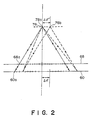
- Figure 2 illustrates an imaging relationship of lights from the mask alignment pattern 68a and the wafer alignment pattern 60a shown in Figure 1.
- a portion of the light divergently advancing from the point 78 is reflectively diffracted by the mask alignment pattern 68a and forms a spot 78a of focused light at or adjacent to the point 78, the spot representing the mask position.
- Another portion of the light passes through the mask 68 in the form of a zero-th order transmission light and is projected upon the wafer alignment pattern 60a on the wafer 60 surface with its wavefront being unchanged.
- the incident light is reflectively diffracted by the wafer alignment pattern 60a and then passes again through the mask 68 in the form of a zero-th order transmission light, and finally is focused in the neighborhood of the point 78 to form a spot 78b of focused light, representing the wafer position.
- the mask 68 functions merely as a transparent member.
- the position of the spot 78b formed by the wafer alignment pattern 60a in the described manner represents a deviation ⁇ ′, in the plane perpendicular to the optical axis containing the point 78, of an amount corresponding to the amount of deviation ⁇ of the wafer 60 with respect to the mask 68.
- an alignment head which is a casing that accommodates therein a light source for producing an alignment light (light to be used for the alignment) is inclined or rotationally displaced relatively to the mask surface, the angle of incidence of the alignment light upon the mask surface changes which causes displacement of the position of the center of gravity of the light upon the sensor surface. Disadvantageously, this necessitate correction of any error component due to relative inclination or rotation of the alignment head and the mask surface, in order to ensure accurate alignment.
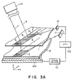
- a first object 1 is a mask, for example, and a second object 2 is a wafer, for example, which is to be aligned with the mask 1.
- First and second alignment marks 5 and 3 are provided on the mask 1 surface and the wafer 2 surface, respectively, for obtaining alignment light.
- Denoted at 6 is a reference mark for obtaining a reference light, which mark is provided on the mask 1 surface (that serves as a reference surface, in this embodiment) at a position adjacent to the first alignment mark 5.
- the first and second alignment marks 3 and 5 and the reference mark 6 each is formed by a grating lens such as a Fresnel zone plate, for example.
- Alignment light (signal light) 7 and reference light 8 emanate from a light source LS accommodated in an alignment head which is not shown. Each of these lights is collimated substantially into a parallel light of a predetermined beam diameter, by means of a projecting lens system (not shown). The lights 7 and 8 are in the form of a single or combined bundle when emitted from the light source, and they are separated by the alignment marks 5 and 6.
- examples that can be used as a light source are: a light source such as a semiconductor laser, a He-Ne laser, an Ar laser or otherwise that can emit a coherent light; and a light source such as a light-emitting diode or otherwise that can emit an incoherent light.
- Sensors (photoreceptors) 11 and 12 function as first and second detecting means, respectively, and are adapted to receive the alignment light 7 and the reference light 8, respectively.
- Each of these sensors may comprise a one-dimensional CCD sensor, for example.
- the one-dimensional CCD sensor is disposed so that the direction in which its sensing elements are arrayed is correlated with the direction with respect to which any positional deviation is to be detected.
- Denoted at 13 is a wafer chuck; at 100 is an X-Y stage; at 101 is a stage driver; and at 102 is a central processing unit (CPU).
- the alignment light 7 and the reference light 8 are incident upon the first alignment mark 5 and the reference mark 6, respectively, on the mask 1 surface, each at a predetermined angle.
- the alignment light 7 is transmissively diffracted by the first alignment mark 5 and then is reflectively diffracted by the second alignment mark 3 on the wafer 2 surface and, finally, is projected on the sensor 11 surface.
- the position of the center of gravity of the light intensity distribution of the alignment light incident on the sensor surface is detected and then, by using an output signal from the sensor 11, the mask 1 and the wafer 2 can be aligned with each other.
- center of gravity of the intensity distribution of light means such a point that, when in the cross-section of the light a position vector of each point in the section is multiplied by the light intensity of that point and the thus obtained products are integrated over the entire section, the integrated value has a "zero vector".
- the position of the peak point in the light intensity may be used as a representative.
- the reference light 8 incident on the reference mark 6 on the first object 1 surface is reflectively diffracted by the reference mark 6.
- the reflectively diffracted light of a predetermined order or orders is converged on the sensor 12 surface.
- the angle of incidence of the reference light 8 on the reference mark 6 is detected.
- the alignment marks 3 and 5 and the reference mark 6 are provided by Fresnel zone plates (or grating lenses) having different focal lengths. Each mark has a size of 140 microns in the lengthwise direction of the scribe line and 50 microns in the widthwise direction (y direction) of the scribe line.
- the alignment light 7 is incident on the mask 1 at an angle of incidence of 10 degrees, with the projection component upon the mask 1 surface being perpendicular to the scribe line direction (x direction).
- the alignment light 7 incident on the mask 1 with a predetermined angle is influenced by the lens function of the grating lens (first alignment mark) 5 and is transformed into a convergent or divergent light which is emitted from the mask 1 so that its chief ray has a predetermined angle with respect to the normal of the mask 1.
- the alignment light 7 having been transmissively diffracted by the first alignment mark 5 is focused at a point of distance of 238.0 microns from the mark, vertically below the wafer 2 surface.
- the alignment mark 5, in this case, has a focal length of 238 microns. Also, the mask 1 and the wafer 2 are spaced by a distance 30 microns.
- the light transmissively diffracted by the alignment mark 5 is influenced by a concave or convex lens function of the second alignment mark 3 on the wafer 2 surface, and is collected on the sensor 11 surface (first detecting means).
- the detector comprises a CCD line sensor having sensing elements arrayed in the X direction.
- the angle of emission of the light emanating from the reference mark 6 of the mask does not change even with any positional deviation between the mask and the wafer, and therefore it is used as a reference light.
- the position of the center of gravity of such reference light upon the sensor 12 is detected and, on the other hand, the position on the sensor 11 of the center of gravity of the alignment light incident on the sensor 11 is detected.
- the interval between these positions in the X direction is measured.
- the measured interval is compared with a reference interval which is the interval in the X-direction between the gravity centers of these two lights as assumed when the mask and the wafer have no relative positional deviation. From the comparison, an error ⁇ is obtainable.
- the thus obtained error ⁇ is substituted into equation (a), whereby the deviation ⁇ can be determined.
- the reference interval can be determined in preparation, for example, geometo-optically from design values of the marks.
- the present embodiment is so set that, when the mask 1 and the wafer 2 have no relative positional deviation (i.e. when the alignment marks 5 and 3 on the mask 1 and the wafer 2 just provide a coaxial system), the chief ray of the alignment light emitting from the wafer 2 has an angle of emission of 5 degrees, and the projection of the emitted light to the wafer 2 surface extends perpendicularly to the widthwise direction (y direction) of the scribe line and, additionally, the emitted light is focused on the sensor 11 surface which is disposed at a predetermined position, for example, at a height of 20 mm from the wafer 2 surface.
- the reflectively diffracted light of the predetermined order or orders (e.g. first order diffraction light), reflectively diffracted by the reference mark 6, has its projection to the mask 1 surface extending orthogonally to the widthwise direction of the scribe line and emanates at an angle of 15 degrees with respect to a normal to the mask 1 surface.
- the sensors 11 and 12 are disposed in parallel to each other.
- the light from the reference mark 6 is focused on the surface of the sensor 12 (second detecting means).
- the first order reflective diffraction light from the reference mark 6, as it is incident on the sensor 12 surface has its position of the center of gravity maintained fixed regardless of any change in the positional deviation between the mask 1 and the wafer 2.
- the grating lens of the reference mark 6 provided on the mask 1 surface has a relatively long focal length, from the reflective diffraction of the reference light by the reference mark on the mask 1 to the impingement to the sensor 12 surface.
- the alignment head is inclined within a section that contains the positional deviation detecting direction (X direction) and a normal to the mask surface, by an amount ⁇ 1 with respect to the normal to the mask surface.
- the distance in that section between the wafer surface and the sensor within the alignment head, in a normal state is denoted by l
- the alignment head is rotated within a section parallel to the mask surface, by an amount ⁇ around the Z axis.
- the angle of incidence (in the Y-Z plane) of the alignment light with respect to the mask surface is denoted by ⁇
- the reference light 8 is within the plane of incidence and, also, the alignment light 7 is present substantially within the plane of incidence. Further, these lights go along optical paths of substantially the same length. Therefore, if the alignment head is inclined, for example, on the sensor 12 surface which is parallel to the sensor 11 surface there occurs exactly the same displacement of the center of gravity as of that of the signal light (alignment light).
- the reference light does not cause displacement of the center of gravity thereof on the sensor with the positional deviation of the wafer to the mask in the X direction (or in the Y direction). In this case, therefore, it can be considered that any displacement of the center of gravity as detected upon the sensor 12 depends only on the inclination or rotation of the alignment head relatively to the mask.
- the value Sg can be detected by using l, g and the magnification m.
- the second correcting method is adopted.
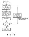
- the flow of the alignment method in this case is illustrated in Figure 3B.
- character A denotes the magnification of the displacement of the center of gravity of light to the actual positional deviation.
- the arrangement may be made so that the difference between the signals Sg and Rg comes equal to a predetermined value, other than zero, and the alignment control may be made accordingly.
- first and second alignment marks 5 and 3 and a reference mark 6 (grating lens) usable in this embodiment can be prepared in the following manner:
- the marks 5 and 6 for a mask are designed so that, when a parallel light of a predetermined beam diameter is incident thereupon at a predetermined angle, the light is collected at a predetermined position.
- a pattern of a grating lens may be that of an interference fringe which can be formed on a lens surface in an occasion where mutually coherent light sources are disposed at a light source position (object point) and the position of an image point.
- a coordinate system is defined on a mask 1 surface, such as shown in Figure 3A.
- Equations regarding a group of curved lines of such a grating lens by which a parallel light, having been incident thereon with an angle ⁇ with respect to the normal of the mask surface 1 and with the projection being perpendicular to the scribe line direction, is imaged after being transmissively or reflectively diffracted by the mark of the mask, at the position of a converging point (x1, y1, z1), can be expressed in the following manner, with the position of each grating line being denoted by x and y: wherein ⁇ is the wavelength of the alignment light and m is an integral number.
- Figure 4A exemplifies a first alignment mark on a mask 1
- Figure 4B exemplifies a first reference mark on the same mask 1.
- a grating lens to be provided on a wafer 2 is designed so as to collect, at a predetermined position (on the sensor surface), a spherical wave emanating from a predetermined point light source.
- a spherical wave emanating from a predetermined point light source is denoted by g.
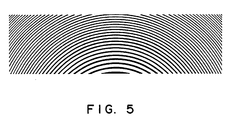
- Figure 5 illustrates a second alignment mark on a wafer 2.
- a zone plate (grating lens) for a mask can be formed as an amplitude type grating element of "0 and 1" in which two regions, a region (transparent portion) that can transmit light and a region (light blocking portion) which does not transmit light, are formed alternately.
- a zone plate for a wafer can be formed as a phase grating pattern having a rectangular section, for example.
- each line of a grating is defined at a position which corresponds to a multiple, by an integral number, of a half wavelength with regard to the chief ray, means that the linewidth ratio of the transparent portion and the light blocking portion is 1:1 in the case of the grating lens on a mask 1, and that the line and space ratio of rectangular grating is 1:1 in the case of the grating lens on the wafer 2.
- a grating lens on a mask 1 was formed by transferring, onto an organic thin film of polyimide, a grating lens pattern of a reticle prepared by use of electron beam exposure technique.
- a mark on a wafer 1 was formed by preparing on a mask a pattern to be printed on a wafer and then by transferring the pattern by use of a lithographic process.
- a sensor which may comprise an accumulation type one-dimensional CCD sensor, for example.
- the reference light and the alignment light emanate from the wafer surface at angles 15 degrees and 5 degrees, respectively, with respect to the normal of the wafer surface and with the projection, upon the wafer surface, being orthogonal to the scribe line direction.
- the spatial disposition of the sensors 11 and 12 is so set that, upon completion of alignment, a light is incident on a corresponding sensor substantially at the middle position.
- the sensors 11 and 12 have a spacing of 2 mm between their centers, and are mounted to a common base plate, made of Si, at a precision of about 0.1 micron.
- the Si base plate on which the sensors 11 and 12 are mounted, is disposed so that its normal extends substantially in parallel to a bisector for the angle of emission of the alignment light and the angle of emission of the reference light, when the mask and the wafer have no relative positional deviation.
- the sensor 11 for the signal light is 1 mm in width and 6 mm in length
- the sensor 12 for the reference light is 1 mm in width and 1 mm in length.
- Each picture element (pixel) has a size of 25 x 500 microns.
- the picture elements are arrayed one-dimensionally in the x-axis direction with respect to which any relative positional deviation of the mask and wafer should be detected.
- Each sensor is operable to measure the position of the center of gravity of incident light, and output signals from the sensor is processed so as to be standardized with regard to the total light quantity over the whole light-receiving region.
- the measured value as outputted from the sensor system exactly represents the position of the center of gravity.
- the resolution of the sensor, for the position of the center of gravity may depend on the power of the alignment light, it was 0.2 micron where a semiconductor laser having a power of 50 mW and a wavelength 0.83 micron was used, by way of example.
- the center of gravity of the signal light displaces along the sensor surface, with the positional deviation between the mask and the wafer being magnified by x100. Therefore, a positional deviation of 0.01 micron between the mask and the wafer results in an effective displacement of the center of gravity on the sensor surface through 1 micron.
- the sensor system can measure such a displacement with a resolution of 0.2 micron.
- the alignment head is inclined within an x-z plane by an amount 1 mrad, there occurs on the sensor 11 a displacement of about 20 microns of the center of gravity of the signal light.
- the sensor 12 there occurs displacement of the center of gravity of the reference light 8 as exactly the same as the signal light.
- both the signal light and the reference light causes displacement of the center of gravity in a direction (widthwise direction) perpendicular to the lengthwise direction of the sensor.
- a displacement is in the direction which is perpendicular to the direction of displacement of the center of gravity of light resulting from the positional deviation (which is just to be detected). Therefore, without the reference light, no practical alignment error occurs.
- the alignment head which may contain an alignment light source, a light projecting lens system and sensors
- a mask and wafer system for example, if the head is displaced by 5 microns in the y direction relatively to a mask
- the center of gravity of the reference light displaces on the sensor 12 by an amount 5 microns, as exactly the same as the signal light.
- FIG 6 is a schematic view of a second embodiment of the present invention.
- a reference light setting means like the first embodiment shown in Figure 3A, as a reference light setting means, a reference mark 6′ formed by a predetermined grating lens is used.
- a mask is provided with a grating lens 5′ which is so set that light incident thereupon at a predetermined angle with respect to the normal to the mask surface is collected at a position which is at a distance 238.0 mm vertically below the mask surface.
- the interval between the mask 1 and a wafer 2 is set to be 30 microns, as in the first embodiment.
- the first alignment mark 5′ and the reference mark 6′ are juxtaposed to each other in the widthwise direction (Y direction) of a scribe line 10.
- the reference mark 6′ has such a focal length that the inputted light from an alignment head, after being reflectively diffracted by the mark with positive or negative first order, is converged at a point which is just on a sensor 12 provided within the alignment head for receiving the reference light.
- the present embodiment is so set that, when the mask 1 and the wafer 2 have no relative positional deviation (i.e. when the alignment marks 5′ and 3′ on the mask 1 and the wafer 2 just provide a coaxial system), the chief ray of the alignment light emitting from the wafer 2 has an angle of emission of 5 degrees, and the projection of the emitted light on the wafer 2 surface extends perpendicularly to the direction (x direction) of the scribe line and, additionally, the emitted light is focused on the sensor 11 surface which is disposed at a predetermined position, for example, at a height of 20 mm from the wafer 2 surface.
- the first order reflective diffraction light, reflected by the reference mark 6′ even if there occurs a change of the positional deviation between the mask 1 and the wafer 2, there does not occur displacement of the position of the center of gravity on the sensor with the misalignment between the grating lenses of the mask and the wafer being magnified, as in the case of the alignment light, and the position of the center of gravity thereof is constantly held fixed.
- the sensors 11 and 12 for the alignment light and the reference light are so set that, when there is no positional deviation between the mask and the wafer, there lights are incident on the respective sensor surfaces perpendicularly.
- the sensors 11 and 12 are formed on a common base plate which is set so that the base plate extends orthogonally to the bisector of the emission angles of the two lights from the wafer (namely, it defines an angle of 6.5 degrees with respect to a normal to the mask or wafer surface).
- the signal light emanating from the wafer surface is substantially kept within the plane of incidence and, also, the reference light is kept within the plane of incidence.
- the optical paths are of the same length.
- any inclination or rotation of the alignment head produces exactly the same displacement of the alignment light and the reference light upon the respective sensors 11 and 12 which are disposed parallel to each other. Similarly, any change in the position of the alignment head does not cause relative shift of the center of gravity, between the alignment light and the reference light.
- the first alignment mark 5′ and the reference mark 6′ each has a size of 280 microns in the direction of the scribe line and 40 microns in the widthwise direction of the scribe line. Also, the alignment is made in respect to the direction of the scribe line.
- the marks on the mark 1 are arrayed in the widthwise direction of the scribe line.
- this embodiment has the following advantageous features as compared with the first embodiment.
- a mark for the signal light and a mark for the reference light are arrayed in the direction of the scribe line.
- the region in which alignment marks are to be set is limited to a certain area (for example, 280 x 80 microns) on the scribe line. As a result, it is not so easy to obtain such a lens as having a focal length in a certain range and having superior imaging performance.
- a region of 280 x 80 microns is uniformly divided in the scribe line direction and a lens is prepared by using a region of 140 x 80 microns with a case where the region is divided in the widthwise direction and a lens is prepared by using a region of 280 x 40 microns
- the imaging performance (resolution) of a zone plate is better with a larger number of gratings and a smaller size of a minimum ring width.
- FIG 7 is a schematic view of a third embodiment of the present invention.
- same reference numerals as of the first embodiment shown in Figure 3A are assigned to corresponding elements.
- first and second alignment marks 5 ⁇ and 3 ⁇ and a reference mark 6 ⁇ used in this embodiment.
- the alignment marks 3 ⁇ and 5 ⁇ and the reference mark 6 ⁇ are provided by Fresnel zone plates (or grating lenses) each having a predetermined focal length. Each mark has a size of 140 microns in the lengthwise direction of the scribe line and 50 microns in the widthwise direction (y direction) of the scribe line.
- both the alignment light 7 and the reference light 8 are incident on the mask 1 at an angle of incidence of 10 degrees, with the projection upon the mask 1 surface being perpendicular to the scribe line direction (x direction).
- the alignment light 7 and the reference light 8 incident on the mask 1 with a predetermined angle are influenced by the lens functions of the grating lenses 5 ⁇ and 6 ⁇ , respectively, each being transformed into a convergent or divergent light which is emitted from the mask 1 so that its chief ray has a predetermined angle with respect to the normal of the mask 1.
- the alignment light 7 having been transmissively diffracted by the first alignment mark 5 ⁇ is collected at a point on the wafer 2 surface which is at a distance of 238.0 microns vertically below the mark.
- the alignment mark 5 ⁇ in this case, has a focal length of 238 microns. Also, the mask 1 and the wafer 2 are spaced by a distance 30 microns.
- the light transmissively diffracted by the alignment mark 5 ⁇ is influenced by a concave or convex lens function of the second alignment mark 3 ⁇ on the wafer 2 surface, and is focused at a point on the sensor 11 surface (first detecting means). On this sensor 11 surface, at this time, the light is incident with any relative positional deviation (i.e. any misalignment of the axes) of the alignment marks 5 ⁇ and 3 ⁇ being magnified, with a result of corresponding shift of the position of the center of gravity of the incident light.
- the present embodiment is so set that, when the mask 1 and the wafer 2 have no relative positional deviation, the chief ray of the alignment light emitting from the wafer 2 has an angle of emission of 5 degrees, and the projection of the emitted light on the wafer 2 surface extends with an angle 2 degrees to the widthwise direction (y direction) of the scribe line and, additionally, the emitted light is focused on the sensor 11 surface which is disposed at a predetermined position, for example, at a height of 20 mm from the wafer 2 surface.
- the arrangement of the present embodiment is set so that the angle of emission of the chief ray of the reference light 8 from the mask 1 surface is equal to 5 degrees, while the projection thereof has an angle of -2 degrees with respect to the widthwise direction of the scribe line 10. Setting the emission angles of the signal light and the reference light to be equal to 2 degrees and -2 degrees, respectively, with respect to the scribe line direction, can assure good separation of the signal light and the reference light on the sensor and thus makes it possible to reduce crosstalk.
- the grating lens of the reference mark 6 ⁇ provided on the mask 1 surface has a relatively long focal length, from the reflection of the reference light by the mask 1 surface to the impingement on the sensor 12 surface of the reference light.
- the one-dimensional sensors 11 and 12 for detecting the positional deviation are formed on a common base plate, as in the first embodiment, which base plate is so set that a normal to the surface of the base plate is coincident with a bisector of the emission angles of the signal light and the reference light from the wafer.
- the mark for the reference light and the mark for the signal light are set in accordance with equations (1) and (2) having been described with reference to the first embodiment.
- the reference light 8 and the alignment light 7 go along respective optical paths of substantially the same length, and the sensor 11 surface and the sensor 12 surface are made parallel to each other. Further, the distance from each alignment mark to the corresponding sensor is sufficiently long, whereas the angle defined by the projection on the X-Y plane of each light with respect to the Y axis or relative to the scribe line is sufficiently small (in this particular example, 2 degrees and -2 degrees). As a result, any change in the angle of emission of each light 7 or 8 due to the inclination or the like of the alignment head produces exactly the same displacement of the center of gravity, on each of the sensors 11 and 12.
- any inclination or rotation of the alignment head or any change in the position of the alignment head, relative to the mask-wafer system can be cancelled, in the manner described hereinbefore, on the basis of a detection signal of the center of gravity as supplied from the sensor receiving the reference light and the detection signal of the gravity center as supplied from the sensor receiving the signal light. Therefore, substantially the same positional deviation detecting performance as of the first embodiment is obtainable.
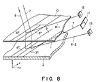
- Figure 8 is a schematic view of a fourth embodiment of the present invention.
- This embodiment corresponds to a combination of the structure of the foregoing embodiment and such structure wherein each of a mask and a wafer is provided with a reference mark for detecting inclination of the wafer, for example, and wherein a reference light receiving sensor is provided in an alignment head.
- the wafer is provided with a mark 4′′′ for reference light and, additionally, a reference light receiving sensor 13 for detecting inclination of the wafer is provided within the alignment head.
- an alignment light receiving sensor 11 as well as a reference light receiving sensor 12, for detecting the attitude of the alignment head are provided in the alignment head, like the first to third embodiments.
- the arrangement of the marks as well as the disposition of the sensors within the head are substantially the same as those in the second embodiment, and the separation of the alignment light and two reference lights 8-1 and 8-2 is made on the basis of the difference in the angle of emission with respect to a normal to the wafer surface.
- the positional deviation detecting direction lies in the direction of the scribe line on the mask (i.e. X direction).
- the central axis of each physical optic lens element as well as the center of gravity of light received by each sensor within the alignment head are within the same plane of the inputted light (i.e. the plane of incidence).
- the mask is provided with a mark 6′′′ for the reference light, which is designed so that the first order reflective diffraction light therefrom is collected and imaged on the sensor 12 within the alignment head, and the reference emission angle with respect to a normal to the mask surface is 5 degrees.
- transmitted first order diffraction light from the mark 6′′′ of the mask for the reference light provides a reference light for detecting the inclination of the wafer, for example, and it is influenced by the first order reflection by the mark 4′′′ of the wafer and is focused on the sensor 13 within the alignment head.
- the mark 4′′′ of the wafer, for the reference light is provided by a rectilinear grating having no lens function, and the angle of emission of the light from the wafer surface is 13 degrees, regardless of the positional deviation between the mask and the wafer.
- Alignment light for detecting the amount of positional deviation is transmissively diffracted at first order, for example, by a grating lens 5′′′ on the mask and, then, is reflectively diffracted at first order by a grating lens 3′′′. Finally, it is transmitted at zero-th order through the mask.
- the angle of emission of the alignment light with respect to a normal to the wafer surface is 9 degrees, and it is received by the sensor 11 in the alignment head.
- the relationship between the signal light 7 and the reference light 8-1 is the same as that between the alignment light 7 and the reference light 8 in the second embodiment, and by using the outputs of the sensors 11 and 12 in the manner described hereinbefore, it is possible to compensate the inclination or otherwise of the alignment head.
- Both of the reference lights 8-1 and 8-2 are in the plane of incidence and, additionally, they go along respective optical paths of substantially the same length. Therefore, any inclination of the alignment head produces exactly the same displacement of the center of gravity upon each of the sensor 12 surface and the sensor 13 surface which are parallel to each other. If the wafer 2 surface includes waviness, inclination or the like, the center of gravity of the reference light 8-2 displaces. However, the center of gravity of the reference light 8-2 does not shift. Therefore, the difference between the signals Rg1 and Rg2, representing the positions of incidence of the lights upon the sensors 12 and 13, respectively, is indicative of the inclination of the wafer.
- the inclination of the wafer can be corrected by moving the wafer stage, for example.
- the positional error as determined on the basis of the output of the sensor 11 may be compensated. In this manner, it is possible to avoid the effect of the inclination of the wafer 2.
- the fourth embodiment it is possible to correct the amount of displacement (resulting in an error factor for the detection of the positional deviation) of the light upon the sensor from its regular position, which is caused when the wafer surface is inclined in the X-Z plane, even locally.
- the correction of the positional deviation detection error due to a change in attitude of the alignment head as described with reference to the foregoing embodiment, it is possible to make overall correction of the mechanical setting error and, therefore, it is possible to ensure high-precision detection of the positional deviation.
- the power arrangement (focal length) of the grating lens for the signal light as well as the positional deviation detecting magnification are set in the same way as in the first to third embodiments.
- the present invention is not limited thereto.
- the alignment light 8 is incident on the mask surface with inclination, and the light emanating from the wafer surface goes at inclination, with the sign of the Y-axis component perpendicular to the scribe line being unchanged (+Y axis direction).
- the invention is not limited to such a structure.
- the inclined emission light from the wafer surface may lie in the -Y axis direction.
- the alignment marks are so arranged that the correct alignment is discriminated when the wafer alignment mark is positioned just underneath the mask alignment mark.
- they may be disposed with mutual shift in a direction perpendicular to the positional deviation detecting direction.
- the width of the alignment mark of the wafer may be shifted in the Y direction, wherein the scribe line direction lies in the X direction.
- the senor is not limited to one that is adapted to detect the positional deviation one-dimensionally, as in the first to fourth embodiments.
- Two-dimensional gravity center detecting sensor such as a two-dimensional CCD, for example, may be used.
- the position of the center of gravity of the light intensity distribution of the alignment light upon the sensor, in respect to the positional deviation detecting direction may be measured.
- a grating lens has a lens function both in the positional deviation detecting direction and in a direction perpendicular thereto, as compared with a case where the grating lens has a lens function only in the positional error detecting direction, use of a two-dimensional sensor makes it possible to obtain positional information in regard to a desired direction.
- the surface of the second object may be used as a reference surface.
- a reference mark may be provided on the second object, and the zero-th order transmission light from the first object may be inputted to the reference mark on the second object.
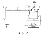
- Figures 9 and 10 are schematic views, respectively, showing optical arrangements of a measuring system and a correcting system in accordance with a fifth embodiment, in which the invention is applied to a device for measuring the interval between a mask and a wafer, in a semiconductor device manufacturing exposure apparatus.
- the measuring system is such a system for measuring, chiefly, the interval between first and second objects
- the correcting system is such a system for correcting a measurement error due to any change in attitude of an illumination system or a light receiving system relatively to the surface of the object.
- reference numerals 21a and 21b denote lights each from a light source LD such as, for example, a He-Ne laser, a semiconductor laser or otherwise. Of these lights, the light 21a is for the measuring system, while the light 21b is for the correcting system.
- a light source LD such as, for example, a He-Ne laser, a semiconductor laser or otherwise. Of these lights, the light 21a is for the measuring system, while the light 21b is for the correcting system.
- First object 1 is a mask, for example, and a second object 2 is a wafer, for example.
- the mask 1 and the wafer 2 are disposed opposed to each other, as illustrated in Figure 9, with a spacing d0.
- Denoted at 4a and 5a are physical optic elements provided in a portion of the mask 1 surface, for light reception and emission in the measuring system. These physical optic elements 4a and 5a each is formed by a diffraction grating or a zone plate, for example. These elements have sizes of about 30 x 30 microns and 30 x 60 microns, respectively.
- denoted at 4b is an physical optic element provided in the correcting system. It has a size of 30 x 30 microns, for example.
- the physical optic element 5a for the light emission in the measuring system has such characteristics that the deflection angle for the emitting light changes depending on the position of incidence of light thereupon and, in this example, it has a refraction power for focusing a received parallel light at a distance of 1000 microns.
- Denoted at 17 is a condensing lense for the measuring system and the correcting system, which has a focal length f a .
- f a is approximately equal to 30 mm.
- Each light receiving means may comprise a line sensor, PSD or otherwise and is adapted to detect the position of center of gravity of light incident thereupon.
- Signal processing circuit 19a operates to determine the positions of lights incident upon the surfaces of the light receiving means 11 and 12, by using signals from these light receiving means, and also to detect, by calculation, the spacing d0 between the mask 1 and the wafer 2 and/or the amount of correction to be made in relation to the inclination of an optical pickup head, which will be described later in detail.
- Denoted generally at 20b is an optical pickup head which accommodates the condensing lens 17, light receiving means 11 and 12 and, if desired, the signal processing circuit 19a.
- the optical head is movable relatively to the mask 1 and wafer 2.
- the reflection light 31 is one as obtainable when the wafer 2 is located at the position P1 close to the mask 1.
- the reflection light 32 is one which is obtainable when the wafer 2 is displaced by a distance d G from the position P1, namely, to the position P2.
- FZP Fresnel zone plate
- the FZP 5a has an optical function for changing the emission angle for the emitted diffraction light in accordance with the position of incidence of the light thereupon.
- Diffraction light 61 (62) of a predetermined order or orders, diffracted at an angle ⁇ 2 from the FZP 5a is directed through the condensing lens 17 to the surface of the light receiving means 11.
- the spacing between the mask 1 and the wafer 2 can be detected by calculation, on the basis of detection of the position of light 61 (62) incident upon the light receiving means 11 surface.
- the first and second physical optic elements 4a and 5a provided on the mask 202 each is formed with a preset pitch, and the diffraction angles ⁇ 1 and ⁇ 2 of the diffraction lights of the predetermined order or orders (for example, ⁇ first order) incident on these plates are detected preparatorily.
- reference light 63 emanates from the mask at a constant angle of emission regardless of any change in the interval between the mask and the wafer.
- the position of the center of gravity of this light upon the sensor is used as a reference. That is, the interval in the X direction between the reference position and the position of the center of gravity of light 61 (62) on the sensor is measured. Then, the measured value is compared with a reference interval which is the interval in the X direction between the positions of the gravity centers of these lights when the wafer is at the position (e.g. P1) of the correct mask-to-wafer interval d R . Any error S detected by this comparison is substituted into equation (9), and the error d G in the interval from the correct interval position P1 of the wafer is detected.
- the reference interval between the gravity centers of the lights 61 (62) and 63 in the X direction as assumed when the correct interval d R is established, can be detected in preparation from the design values of the marks, for example.
- the light (spot) on the light receiving means 11 surface displaces by 18 microns.
- the gap between the mask 1 and the wafer 2 can be measured with the resolution not greater than 0.02 micron.
- the condensing lens 17 is disposed in front of the light receiving means 11 of the measuring system.
- the lens 17 may be omitted.
- the distance from the physical optic element 5a of the mask 1 to the light receiving means 12 is denoted by la
- f a l a
- Light 21b is incident on the physical optic element 4b provided on the mask 1, for light reception.
- the physical optic element 4b has such optical characteristics that, when a parallel light is incident thereon, it emits a diffraction light at a certain deflection angle in accordance with the angle of incidence of the light, but independently of the position of incidence of the light.
- Light 21b emanating from the semiconductor laser LD is incident with inclination on the grating 4b, at a predetermined angle with respect to a normal to the mask surface, as illustrated in the drawing.
- positive first order reflective diffraction light 63 is received by the light receiving means 12 provided within an optical pickup head (not shown).
- the grating 4b is formed by a pattern of rectilinear grating parallel to an X axis of an orthogonal coordinate system having its X axis extending in the lengthwise direction of a rectangular interval measuring mark region and having its Y axis extending in the widthwise direction of the mark region.
- Figures 11A and 11B show the optical path of the light 21b, in an X-Z section and in a Y-Z section, respectively.
- the light spot position detecting direction of the reference-light receiving means 12 is parallel to the X axis and agrees to the light spot position detecting direction of the measuring-light receiving means 11.
- the reference light 21b can be used to correct any error in the measurement of the interval, due to any shift of the optical pickup head 20 which accommodates therein the light source LD, the light receiving means 11 and 12 and the like, or due to any change in the angle (attitude) of the alignment head relative to the mask, as resulting from the replacement of the mask, for example. More specifically, the lights 61 (62) and 63 go along respective optical paths having substantially the same length and impinge on the sensor surfaces 11 and 12 which are parallel to each other. In practical measurement of the mask-to-wafer interval, the light 61 (62) is substantially parallel to the light 63.
- the physical optic element 5a of the correcting system may have a function of a lens element.
- a lens element For example, when a grating lens having a focal length corresponding to the distance to the sensor surface is used, with the condensing function of such a lens it is possible to increase the density of the intensity distribution of the interval detecting light upon the sensor to thereby improve the signal-to-noise ratio.
Landscapes
- Physics & Mathematics (AREA)
- General Physics & Mathematics (AREA)
- Exposure And Positioning Against Photoresist Photosensitive Materials (AREA)
- Exposure Of Semiconductors, Excluding Electron Or Ion Beam Exposure (AREA)
- Length Measuring Devices By Optical Means (AREA)
Applications Claiming Priority (4)
| Application Number | Priority Date | Filing Date | Title |
|---|---|---|---|
| JP22153788 | 1988-09-05 | ||
| JP221537/88 | 1988-09-05 | ||
| JP209925/89 | 1989-08-14 | ||
| JP1209925A JP2676933B2 (ja) | 1988-09-05 | 1989-08-14 | 位置検出装置 |
Publications (2)
| Publication Number | Publication Date |
|---|---|
| EP0358425A2 true EP0358425A2 (fr) | 1990-03-14 |
| EP0358425A3 EP0358425A3 (fr) | 1990-12-27 |
Family
ID=26517753
Family Applications (1)
| Application Number | Title | Priority Date | Filing Date |
|---|---|---|---|
| EP19890308921 Withdrawn EP0358425A3 (fr) | 1988-09-05 | 1989-09-04 | Méthode et dispositif de détection de position |
Country Status (2)
| Country | Link |
|---|---|
| EP (1) | EP0358425A3 (fr) |
| JP (1) | JP2676933B2 (fr) |
Cited By (10)
| Publication number | Priority date | Publication date | Assignee | Title |
|---|---|---|---|---|
| EP0455446A3 (en) * | 1990-05-01 | 1992-07-08 | Canon Kabushiki Kaisha | Position detecting method and apparatus |
| EP0488798A3 (en) * | 1990-11-30 | 1992-12-02 | Canon Kabushiki Kaisha | Position detecting method |
| EP0534758A1 (fr) * | 1991-09-27 | 1993-03-31 | Canon Kabushiki Kaisha | Méthode et appareil pour la mesure des écarts de position |
| US5200800A (en) * | 1990-05-01 | 1993-04-06 | Canon Kabushiki Kaisha | Position detecting method and apparatus |
| EP0439322B1 (fr) * | 1990-01-23 | 1996-11-27 | Canon Kabushiki Kaisha | Méthode et dispositif de mesure de l'écartement de deux objets opposés |
| EP0752600A3 (fr) * | 1995-07-06 | 1997-08-27 | Dainippon Printing Co Ltd | Filtre coloré holographique et son procédé de fabrication |
| WO2002035288A1 (fr) * | 2000-10-23 | 2002-05-02 | Advanced Micro Devices, Inc. | Systeme et procede destines a faciliter l'alignement des plaquettes, permettant d'attenuer les effets de rotation du reticule sur le recouvrement |
| US6552790B1 (en) | 2001-02-20 | 2003-04-22 | Advanced Micro Devices, Inc. | System and method for facilitating wafer alignment by mitigating effects of reticle rotation on overlay |
| US9959610B2 (en) | 2014-10-30 | 2018-05-01 | Applied Materials, Inc. | System and method to detect substrate and/or substrate support misalignment using imaging |
| CN111380509A (zh) * | 2018-12-28 | 2020-07-07 | 上海微电子装备(集团)股份有限公司 | 一种掩模版姿态监测方法、装置及掩模版颗粒度检测设备 |
Families Citing this family (1)
| Publication number | Priority date | Publication date | Assignee | Title |
|---|---|---|---|---|
| KR102863372B1 (ko) * | 2019-02-28 | 2025-09-24 | 에이에스엠엘 네델란즈 비.브이. | 레티클 조립체의 조립을 위한 장치 |
Citations (2)
| Publication number | Priority date | Publication date | Assignee | Title |
|---|---|---|---|---|
| US4326805A (en) * | 1980-04-11 | 1982-04-27 | Bell Telephone Laboratories, Incorporated | Method and apparatus for aligning mask and wafer members |
| US4360273A (en) * | 1980-02-14 | 1982-11-23 | Sperry Corporation | Optical alignment of masks for X-ray lithography |
Family Cites Families (4)
| Publication number | Priority date | Publication date | Assignee | Title |
|---|---|---|---|---|
| US4037969A (en) * | 1976-04-02 | 1977-07-26 | Bell Telephone Laboratories, Incorporated | Zone plate alignment marks |
| US4472824A (en) * | 1982-08-04 | 1984-09-18 | The Perkin-Elmer Corporation | Apparatus for effecting alignment and spacing control of a mask and wafer for use in X-ray lithography |
| DE68925142T2 (de) * | 1988-02-16 | 1996-06-13 | Canon K.K., Tokio/Tokyo | Vorrichtung zum Nachweis der örtlichen Beziehung zwischen zwei Objekten |
| JP2513300B2 (ja) | 1988-02-16 | 1996-07-03 | キヤノン株式会社 | 位置検出装置 |
-
1989
- 1989-08-14 JP JP1209925A patent/JP2676933B2/ja not_active Expired - Fee Related
- 1989-09-04 EP EP19890308921 patent/EP0358425A3/fr not_active Withdrawn
Patent Citations (2)
| Publication number | Priority date | Publication date | Assignee | Title |
|---|---|---|---|---|
| US4360273A (en) * | 1980-02-14 | 1982-11-23 | Sperry Corporation | Optical alignment of masks for X-ray lithography |
| US4326805A (en) * | 1980-04-11 | 1982-04-27 | Bell Telephone Laboratories, Incorporated | Method and apparatus for aligning mask and wafer members |
Cited By (14)
| Publication number | Priority date | Publication date | Assignee | Title |
|---|---|---|---|---|
| EP0439322B1 (fr) * | 1990-01-23 | 1996-11-27 | Canon Kabushiki Kaisha | Méthode et dispositif de mesure de l'écartement de deux objets opposés |
| US5200800A (en) * | 1990-05-01 | 1993-04-06 | Canon Kabushiki Kaisha | Position detecting method and apparatus |
| EP0455446A3 (en) * | 1990-05-01 | 1992-07-08 | Canon Kabushiki Kaisha | Position detecting method and apparatus |
| EP0488798A3 (en) * | 1990-11-30 | 1992-12-02 | Canon Kabushiki Kaisha | Position detecting method |
| US5396335A (en) * | 1990-11-30 | 1995-03-07 | Canon Kabushiki Kaisha | Position detecting method |
| US5751426A (en) * | 1991-09-27 | 1998-05-12 | Canon Kabushiki Kaisha | Positional deviation measuring device and method for measuring the positional deviation between a plurality of diffraction gratings formed on the same object |
| EP0534758A1 (fr) * | 1991-09-27 | 1993-03-31 | Canon Kabushiki Kaisha | Méthode et appareil pour la mesure des écarts de position |
| EP0752600A3 (fr) * | 1995-07-06 | 1997-08-27 | Dainippon Printing Co Ltd | Filtre coloré holographique et son procédé de fabrication |
| US6426812B2 (en) | 1995-07-06 | 2002-07-30 | Dai Nippon Printing Co., Ltd. | Hologram color filter, and its fabrication method |
| EP1367415A3 (fr) * | 1995-07-06 | 2004-08-18 | Dai Nippon Printing Co., Ltd. | Filtre coloré holographique et son procédé de fabrication |
| WO2002035288A1 (fr) * | 2000-10-23 | 2002-05-02 | Advanced Micro Devices, Inc. | Systeme et procede destines a faciliter l'alignement des plaquettes, permettant d'attenuer les effets de rotation du reticule sur le recouvrement |
| US6552790B1 (en) | 2001-02-20 | 2003-04-22 | Advanced Micro Devices, Inc. | System and method for facilitating wafer alignment by mitigating effects of reticle rotation on overlay |
| US9959610B2 (en) | 2014-10-30 | 2018-05-01 | Applied Materials, Inc. | System and method to detect substrate and/or substrate support misalignment using imaging |
| CN111380509A (zh) * | 2018-12-28 | 2020-07-07 | 上海微电子装备(集团)股份有限公司 | 一种掩模版姿态监测方法、装置及掩模版颗粒度检测设备 |
Also Published As
| Publication number | Publication date |
|---|---|
| JPH02167409A (ja) | 1990-06-27 |
| EP0358425A3 (fr) | 1990-12-27 |
| JP2676933B2 (ja) | 1997-11-17 |
Similar Documents
| Publication | Publication Date | Title |
|---|---|---|
| EP0409572B1 (fr) | Système de détection de position | |
| EP0411966B1 (fr) | Méthode et dispositif de détection de position | |
| EP0329430B1 (fr) | Dispositif de détection de position | |
| US6297876B1 (en) | Lithographic projection apparatus with an alignment system for aligning substrate on mask | |
| EP0409573B1 (fr) | Méthode pour la détection des écarts en position | |
| US5200800A (en) | Position detecting method and apparatus | |
| US5235408A (en) | Position detecting method and apparatus | |
| EP0358425A2 (fr) | Méthode et dispositif de détection de position | |
| US5160848A (en) | Device for detecting the relative position between opposed first and second objects | |
| EP0439322B1 (fr) | Méthode et dispositif de mesure de l'écartement de deux objets opposés | |
| US5225892A (en) | Positional deviation detecting method | |
| US5325176A (en) | Position detecting method and apparatus including Fraunhofer diffraction detector | |
| EP0336537A1 (fr) | Dispositif pour détecter la relation de la position entre deux objets | |
| US5294980A (en) | Positioning detecting method and apparatus | |
| JP2513300B2 (ja) | 位置検出装置 | |
| EP0358511B1 (fr) | Dispositif de détection de la relation de position de deux objets | |
| US5148035A (en) | Position detecting method and apparatus | |
| EP0329433A2 (fr) | Méthode et appareil pour détection de position | |
| JP2827250B2 (ja) | 位置検出装置 | |
| JP2513282B2 (ja) | 位置合わせ装置 | |
| JP2623757B2 (ja) | 位置合わせ装置 | |
| JP2836180B2 (ja) | 位置検出装置 | |
| JP2513301B2 (ja) | 位置検出装置 | |
| JP2924178B2 (ja) | 位置検出装置 | |
| JPH021509A (ja) | 位置検出装置 |
Legal Events
| Date | Code | Title | Description |
|---|---|---|---|
| PUAI | Public reference made under article 153(3) epc to a published international application that has entered the european phase |
Free format text: ORIGINAL CODE: 0009012 |
|
| AK | Designated contracting states |
Kind code of ref document: A2 Designated state(s): DE FR GB NL |
|
| PUAL | Search report despatched |
Free format text: ORIGINAL CODE: 0009013 |
|
| AK | Designated contracting states |
Kind code of ref document: A3 Designated state(s): DE FR GB NL |
|
| 17P | Request for examination filed |
Effective date: 19901231 |
|
| 17Q | First examination report despatched |
Effective date: 19930709 |
|
| STAA | Information on the status of an ep patent application or granted ep patent |
Free format text: STATUS: THE APPLICATION HAS BEEN WITHDRAWN |
|
| 18W | Application withdrawn |
Effective date: 20080801 |