EP0358476B1 - Integrierte optische Bauteile - Google Patents
Integrierte optische Bauteile Download PDFInfo
- Publication number
- EP0358476B1 EP0358476B1 EP89309013A EP89309013A EP0358476B1 EP 0358476 B1 EP0358476 B1 EP 0358476B1 EP 89309013 A EP89309013 A EP 89309013A EP 89309013 A EP89309013 A EP 89309013A EP 0358476 B1 EP0358476 B1 EP 0358476B1
- Authority
- EP
- European Patent Office
- Prior art keywords
- polymeric material
- irradiation
- layer
- sidegroups
- integrated optic
- Prior art date
- Legal status (The legal status is an assumption and is not a legal conclusion. Google has not performed a legal analysis and makes no representation as to the accuracy of the status listed.)
- Expired - Lifetime
Links
Images

Classifications
-
- G—PHYSICS
- G02—OPTICS
- G02F—OPTICAL DEVICES OR ARRANGEMENTS FOR THE CONTROL OF LIGHT BY MODIFICATION OF THE OPTICAL PROPERTIES OF THE MEDIA OF THE ELEMENTS INVOLVED THEREIN; NON-LINEAR OPTICS; FREQUENCY-CHANGING OF LIGHT; OPTICAL LOGIC ELEMENTS; OPTICAL ANALOGUE/DIGITAL CONVERTERS
- G02F1/00—Devices or arrangements for the control of the intensity, colour, phase, polarisation or direction of light arriving from an independent light source, e.g. switching, gating or modulating; Non-linear optics
- G02F1/01—Devices or arrangements for the control of the intensity, colour, phase, polarisation or direction of light arriving from an independent light source, e.g. switching, gating or modulating; Non-linear optics for the control of the intensity, phase, polarisation or colour
- G02F1/061—Devices or arrangements for the control of the intensity, colour, phase, polarisation or direction of light arriving from an independent light source, e.g. switching, gating or modulating; Non-linear optics for the control of the intensity, phase, polarisation or colour based on electro-optical organic material
- G02F1/065—Devices or arrangements for the control of the intensity, colour, phase, polarisation or direction of light arriving from an independent light source, e.g. switching, gating or modulating; Non-linear optics for the control of the intensity, phase, polarisation or colour based on electro-optical organic material in an optical waveguide structure
-
- G—PHYSICS
- G02—OPTICS
- G02B—OPTICAL ELEMENTS, SYSTEMS OR APPARATUS
- G02B6/00—Light guides; Structural details of arrangements comprising light guides and other optical elements, e.g. couplings
- G02B6/10—Light guides; Structural details of arrangements comprising light guides and other optical elements, e.g. couplings of the optical waveguide type
- G02B6/12—Light guides; Structural details of arrangements comprising light guides and other optical elements, e.g. couplings of the optical waveguide type of the integrated circuit kind
- G02B6/122—Basic optical elements, e.g. light-guiding paths
- G02B6/1221—Basic optical elements, e.g. light-guiding paths made from organic materials
-
- G—PHYSICS
- G03—PHOTOGRAPHY; CINEMATOGRAPHY; ANALOGOUS TECHNIQUES USING WAVES OTHER THAN OPTICAL WAVES; ELECTROGRAPHY; HOLOGRAPHY
- G03F—PHOTOMECHANICAL PRODUCTION OF TEXTURED OR PATTERNED SURFACES, e.g. FOR PRINTING, FOR PROCESSING OF SEMICONDUCTOR DEVICES; MATERIALS THEREFOR; ORIGINALS THEREFOR; APPARATUS SPECIALLY ADAPTED THEREFOR
- G03F7/00—Photomechanical, e.g. photolithographic, production of textured or patterned surfaces, e.g. printing surfaces; Materials therefor, e.g. comprising photoresists; Apparatus specially adapted therefor
- G03F7/0005—Production of optical devices or components in so far as characterised by the lithographic processes or materials used therefor
- G03F7/001—Phase modulating patterns, e.g. refractive index patterns
Definitions
- This invention relates to integrated optic components.
- Passive integrated optic components are well known and comprise a substrate one surface of which carries a refractive index pattern which defines the nature of the component. Typical patterns define waveguide circuits, waveguide gratings, and optical couplers.
- Typical patterns define waveguide circuits, waveguide gratings, and optical couplers.
- Other processing techniques proposed include laser beam writing or contact printing or holographic exposure. The materials which have been proposed, for example as described in 'Light Guiding Structures of Photoresist Films' Appl. Phys. Lett. Vol.
- Active integrated optic components are also well known being fabricated in electro-optic material such as lithium niobate whereby the in-use function of the component is controllable by an external electrical field. It has recently been proposed to fabricate active integrated optic components using a thin film of suitable electro-optic material carried by one surface of a substrate, for example as described in 'Poled electro-optic waveguide formation in thin film organic media' Appl. Phys. Lett. Vol. 52 page 1031 et seq but the method therein described has the disadvantage that the guide properties and electro-optic interaction are combined and optimisation for both efficient guide formation and efficient guide operation under the electro-optic effect cannot be achieved.
- an integrated optic component comprising a substrate carrying on at least one surface thereof a thin film of a polymeric material having the possibility to be made electro-optic, characterised in that the polymeric material has an aliphatic or aromatic polymer backbone with bonded sidegroups exhibiting a hyperpolarizability, and that the material shows a refractive index pattern induced by irradiation with wavelengths within the electronic absorption bands of the sidegroups.
- the sidegroups may be bonded to the backbone either directly or via a spacer, or the sidegroups may be partly incorporated in the backbone.
- the aliphatic or aromatic polymer backbone may take any one of a number of different forms, for example, polyurethane, polyesters, polyacrylates, polyamides, polyethers or polysiloxanes.
- the sidegroups may comprise 4'-amino or 4'-oxy substituted 4-nitrostilbene moieties, or 4'-amino substituted 4-cyanostilbene moieties, or N-substituted 1-(4-amino-phenyl)-4-(4-nitrophenyl) buta-1, 3-diene moieties, for example 4'-amino substituted 4-nitrostilbene.
- the invention is also related to a method of manufacturing an integrated optic component comprising a substrate carrying on at least one side thereof a thin layer of a polymeric material having the possibility to be made electro-optic.
- This method is characterised in that as polymeric material a material is chosen having an aliphatic or aromatic backbone with bonded sidegroups exhibiting hyperpolarizability, and that into said polymeric material a refractive index pattern is induced by selectively exposing said material with irradiation with wavelengths within the electronic absorption bands of the sidegroups.
- the processing time for obtaining usable refractive index patterns is substantially reduced, being of the order of a few tens of minutes (e.g. 50 minutes) and the duration of the refractive index pattern is at least in the order of years.
- the refractive index of the polymeric material is sensitive to irradiation in the waveband 230 to 650 nm, displays increased sensitivity with respect to refractive index changes in comparison to the known materials (by a factor of 10) and may in addition have electro-optic properties. Accordingly fabrication of the component of the present invention is achieved in a manner similar to that previously used for passive components but, with poling, produces an active component. Both efficient guide formation and efficient guide operation are thereby achieved in an active component.
- the selective exposure of the polymeric material to the irradiation may be performed by a selective "writing" procedure, e.g., by a focussed laser beam or by holographic means.
- a selective "writing" procedure e.g., by a focussed laser beam or by holographic means.
- the selective exposure occurs by means of a mask having parts which are transparent and parts which are opaque to the applied irradiation.
- Another aspect of the present invention comprises the fabrication of an active integrated optic component including the steps of successively forming on a substrate a first layer of electrode material, a first layer of buffer material, a layer of the polymeric material, a second layer of buffer material, and a second layer of electrode material, etching the second layer of electrode material to form an electrode of predetermined pattern, and directing irradiation with wavelengths within the electronic absorption bands of the sidegroups onto the exposed surface of the component to cause a change of the refractive index of those areas of the polymeric material which are not covered by the electrode of predetermined pattern, the buffer material of at least the second buffer material layer being non-opaque to the directed irradiation.
- the present invention also comprises the fabrication of a passive integrated optic component, including the steps of forming on a substrate a layer of polymeric material having an aliphatic or aromatic polymer backbone with bonded sidegroups exhibiting a hyperpolarizability, irradiating the polymeric material partway over its thickness with irradiation with wavelengths within the electronic absorption bands of the sidegroups confined to a first predetermined pattern so as to cause a change of the refractive index of those areas of the polymeric material which are so exposed, applying a thin film of said polymeric material dissolved in a solvent to the surface of the polymeric material exposed to said irradiation for a measured time interval so as to dissolve the exposed area of index-changed material, and thereafter washing off the thin film to leave a relief surface structure which is free of index-changed material on the polymeric material.
- the irradiation is applied to the polymeric material when the latter is at an elevated temperature since it has been discovered that the processing time for obtaining a particular refractive index pattern decreases as temperature increases.
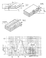
- a substrate 10 having a refractive index of value n 1 is provided on its upper surface with a thin film or layer of polymer material 11.
- the material 11 has a polyurethane backbone to which side groups are chemically bonded, the side groups consisting of 4'-amino or 4'-oxy substituted 4 nitrostilbene, namely 4-nitro-4' aminostilbene or 4-nitro-4' oxystilbene.
- the side groups of the polymer material confer to the material a refractive index sensitivity so that prior to suitable irradiation the material is of uniform refractive index value n 2 but upon irradiation of selected areas of the polymer material with radiation in the 230-650 nm waveband the exposed areas are left with a refractive index of value n 3 (which is less than n 2 ).
- the irradiated areas are selected by a mask 12 having non-transmitting lines 13 thereon so that the radiation is transmitted by the mask between the lines 13 and thereby (as shown in Fig. 3) produces lines 14 on the polymer material 11 of index value n 3 separated by lines 15 of index value n 2 all carried by the substrate of index value n 1 and n 2 >n 3 >n 1 .
- the polymer material which has been described exhibits refractive index sensitivity in the wavelength range 280-450 nm which is particularly useful since it enables exposure by UV sources, for instance in mask aligners thereby facilitating integrated optic components to be fabricated with excellent reproducability, with a slightly-graded or sharp transition in the index profile at the n 2 /n 3 interface which along the length of the transition is smooth and uniform from guide to guide.
- the waveguides thus formed are of relatively low loss per unit length.
- the processing time for irradiation is of the order of a few tens of minutes and because the side groups of the polymer material are bonded to the backbone, it has been found that the irradiated pattern is stable insofar as it is effectively permanently recorded.
- the side groups of the polymer materials described display electro-optic characteristics as a result of which the integrated optic components, after poling, can be electrically operated during use by means of electrodes 16 deposited thereon (Fig. 3), for example to form an electro-optic modulator or other active component.
- Figs. 1 to 3 are schematic and indicate that the irradiation exposure is applied for a sufficient duration to cause conversion of the whole depth of the n 2 index material to n 3 index but for most integrated optic applications it is sufficient to expose for a duration sufficient to effect only a predetermined depth of n 3 index within the body of n 2 index as is illustrated in Fig. 4.
- Fig. 5 illustrates comparative graphs of exposure time and depth for two temperatures, 20°C and 130°C.
- the polymeric material 11 behaves like a photoresist in that after patterning by irradiation exposure as explained with reference to Fig. 4 the n 2 /n 3 index pattern can be converted to a relief pattern of n 2 index by dissolving out the n 3 index areas simply by coating the n 2 /n 3 index pattern with a developer in the form of a thin uniform film of the polymeric material dissolved in a suitable solvent such as cyclopentanone. After a period of time dependant upon the depth of the n 3 index areas the excess developer is removed for example by spinning to leave a layer of the n 2 index material with a relief pattern as shown in Fig. 6.
- the resultant integrated optic component can be used as a raised ridge guide, or as a waveguide taper structure or as a surface relief hologram.
- the component As has been indicated with reference to Fig. 3 if the component is to be used as an active optic component it requires electrodes 16.
- the electrodes 16 of Fig. 3 are essentially co-planar with the lines 15 of n 2 index and they interfere with the process of poling the material 11 which, of course, is necessary to align the side groups of the polymeric material so that its inherent electro-optic capabilities are usable.
- a preferred electrode arrangement is the plane-parallel format illustrated in Fig. 7 and which is manufactured as indicated in Figs. 8 and 9.
- the material 11 suitably index patterned as will be explained is separated from upper and lower electrodes 20, 21, by inactive buffer layers 22A, 22B.
- This is achieved by constructing on the substrate 10 the layered structure shown in Fig. 8 with the upper electrode 20 initially of the same area as the lower electrode 21.
- the material 11 is first poled by applying a poling voltage across the electrodes 20, 21, with the material 11 at elevated temperature. This aligns the side groups of the material 11.
- the upper electrode 20 is patterned by dissolving out the unrequired metal.
- Buffer layer 22A acts as a chemical barrier during this process and the structure has the form shown in Fig. 9.
- irradiation is applied over the whole area of the top surface of the Fig.
- n 1 index areas exposed to the irradiation to n 3 index areas and the only non-exposed n 2 area is that underlying the patterned electrode 20 as shown in Fig. 7.
- the electrode 20 is made of metal, for example gold
- the buffer layer 22A is non-opaque to the radiation, being made for example of polyurethane.
- component electrode 21 is omitted as is the step of poling the polymeric material 11.
- the resultant component is rendered thermoactive by current flow along the top conductor 20.
- the irradiation which has been referred to hereinbefore is preferably in the range between about 250 to 570 nm.
- the main effects however are apparent in the range of about 280 to 450 nm.
- irradiation at about 373 nm results in a maximum sensitivity to refractive index changes.
- irradiation at about 429 nm has provided excellent results both with respect to refractive index changes and low optical losses at the operating wavelength.
- Fig. 10 illustrates the absorption spectrum of one tested sample of the amino substituted polymeric material illustrating that absorption peaks occur at 300 nm and 430 nm which are primarily due to the electronic absorption bands of the sidegroups of the material.
Landscapes
- Physics & Mathematics (AREA)
- General Physics & Mathematics (AREA)
- Optics & Photonics (AREA)
- Nonlinear Science (AREA)
- Engineering & Computer Science (AREA)
- Microelectronics & Electronic Packaging (AREA)
- Optical Integrated Circuits (AREA)
- Compositions Of Macromolecular Compounds (AREA)
- Glass Compositions (AREA)
- Addition Polymer Or Copolymer, Post-Treatments, Or Chemical Modifications (AREA)
- Treatments Of Macromolecular Shaped Articles (AREA)
Claims (17)
- Integrierte optische Komponente mit einem Substrat, das auf mindestens einer seiner Seiten einen dünnen Film eines polymeren Materials trägt, welches die Fähigkeit besitzt, elektrooptisch gemacht zu werden, dadurch gekennzeichnet, dass das polymere Material eine aliphatische oder aromatische Polymergrundkette mit daran hängenden Seitengruppen besitzt, die eine Hyperpolarisierbarkeit aufweisen, und dass das Material bei Bestrahlung mit Wellenlängen in den elektronischen Absorptionsbanden der Seitengruppen ein Brechungsindexmuster zeigt.
- Integrierte optische Komponente nach Anspruch 1, dadurch gekennzeichnet, dass die hyperpolarisierbaren Seitengruppen aus einem System folgender Struktur bestehen:
- i =
- eine cyclische, konjugierte Gruppe, z.B. Phenyl
- R1 =
- -O-, N-,
-S-, oder
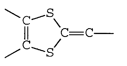
- k =
- Null bis einschliesslich 4
- R2 =
- oder N

- R =
- Wasserstoff, Halogen, Cyan oder Niederalkyl
- m =
- Null bis einschliesslich 6
- j =
- eine cyclische konjugierte Gruppe, z.B. Phenyl
- l =
- Null bis einschliesslich 4
- R4 =
- oder N
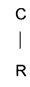
- R5 =
- oder N

- n =
- Null bis einschliesslich 6
- R6 =
- -CN,
oder-C = C - R8

- R7 =
- Alkyl
- R8 =
- H oder -CN
- Rg =
- H oder -CN
- R10 =
- H oder -CN
- Integrierte optische Komponente nach Anspruch 2, dadurch gekennzeichnet, dass die Seitengruppen 4'-amino- oder 4'-oxysubstituierte 4-Nitrostilbeneinheiten oder 4'-amino-substituierte 4-Cyanostilbengruppen oder N-substituierte 1-(4-Aminophenyl)-4-(4-nitrophenyl)-buta-1,3-diengruppen enthalten.
- Integrierte optische Komponente nach Anspruch 3, dadurch gekennzeichnet, dass die Seitengruppen aus 4'-aminosub-stituiertem 4-Nitrostilben bestehen.
- Integrierte optische Komponente nach einem der Ansprüche 1 bis 4, dadurch gekennzeichnet, dass das polymere Material ein durch Bestrahlen mit einer Wellenlänge im Bereich von etwa 230 bis 650 nm induziertes Brechungsindexmuster besitzt.
- Integrierte optische Komponente nach Anspruch 5, dadurch gekennzeichnet, dass das polymere Material ein durch Bestrahlen mit einer Wellenlänge im Bereich von etwa 250 bis 570 nm induziertes Brechungsindexmuster zeigt.
- Integrierte optische Komponente nach Anspruch 6, dadurch gekennzeichnet, dass das polymere Material ein durch Bestrahlung mit einer Wellenlänge im Bereich von etwa 280 bis 450 nm induziertes Brechungsindexmuster zeigt.
- Verfahren zur Herstellung einer integrierten optischen Komponente nach einem der vorangehenden Ansprüche 1-7, wobei in dem polymeren Material durch selektives Belichten des Materials bei einer Bestrahlung mit Wellenlängen innerhalb der elektronischen Absorptionsbanden der Seitengruppen ein Brechungsindexmuster induziert wird.
- Verfahren nach Anspruch 8, bei dem das polymere Material teilweise über seine Dicke bestrahlt wird, ein dünner Film des polymeren Materials, gelöst in einem Lösungsmittel, auf die Oberfläche des der Strahlung während eines bestimmten Zeitintervalls ausgesetzten polymeren Materials aufgetragen wird, um den belichteten Bereich des Materials mit verändertem Index zu lösen, und wobei der dünne Film von dem Film abgewaschen wird, um eine Relief-Oberflächenstruktur zurückzulassen, die frei von indexverändertem Material auf dem polymeren Material ist.
- Verfahren nach Anspruch 9, bei welchem auf der Relief-oberflächenstruktur eine zweite Schicht aus Puffermaterial und eine zweite Schicht aus Elektrodenmaterial gebildet wird und bei welchem das polymere Material durch Anlegen einer Polungsspannung zwischen der ersten und zweiten Schicht aus Elektrodenmaterial gepolt wird.
- Verfahren nach Anspruch 10, gekennzeichnet durch den Schritt des Ätzens der zweiten Schicht aus Elektrodenmaterial in einem zweiten vorbestimmten Muster, was in Beziehung steht zu dem ersten vorbestimmten Muster vor dem Polen.
- Verfahren nach Anspruch 8, gekennzeichnet durch die Schritte des nacheinanderfolgenden Bildens auf einem Substrat einer ersten Schicht aus Elektrodenmaterial, einer ersten Schicht aus Puffermaterial, einer Schicht des polymeren Materials, einer zweiten Schicht aus Puffermaterial und einer zweiten Schicht aus Elektrodenmaterial, Ätzen der zweiten Schicht aus Elektrodenmaterial zur Bildung einer Elektrode mit vorbestimmtem Muster und Richten von Strahlung mit Wellenlängen innerhalb der elektronischen Absorptionsbanden der Seitengruppen auf die belichtete Oberfläche der Komponente, um eine Veränderung des Brechungsindex derjenigen Bereiche des polymeren Materials zu bewirken, die nicht durch die Elektrode mit vorbestimmtem Muster bedeckt sind, wobei das Puffermaterial mindestens der zweiten Puffermaterialschicht für die gerichtete Strahlung nicht undurchlässig ist.
- Verfahren nach Anspruch 12, gekennzeichnet durch den Schritt des Polens des polymeren Materials durch Anlegen einer Polungsspannung zwischen der ersten und zweiten Elektrodenmaterialschicht vor dem Ätzschritt, wodurch eine aktive integrierte optische Komponente hergestellt wird.
- Verfahren nach Anspruch 13, gekennzeichnet durch den Schritt des lokalen Polens des polymeren Materials durch Anlegen einer Polungsspannung zwischen der ersten und zweiten Elektrodenmaterialschicht nach dem Ätzschritt.
- Verfahren zur Herstellung eines Arrays aus integrierten optischen Komponenten, welches Verfahren gekennzeichnet ist durch die Schritte der Durchführung des Verfahrens von Anspruch 8, wodurch die selektive Belichtung den Komponentenarray definiert, Testen der Eigenschaften der einzelnen Komponenten in dem Array zur Identifikation derjenigen Komponenten mit unerwünschten Eigenschaften und Abstimmung solcher Komponenten, um die gewünschten Eigenschaften durch lokale Applikation weiterer Bestrahlung zu erzeugen.
- Verfahren nach einem der Ansprüche 8-11 und 15, bei welchem die selektive Belichtung mittels einer Maske erfolgt, die Teile besitzt, welche für die applizierte Bestrahlung transparent sind, und solche Teile, die nicht transparent sind.
- Verfahren nach einem der Ansprüche 8 bis 16, bei welchem die Bestrahlung auf das polymere Material zur Einwirkung gebracht wird, wenn sich letzteres auf einer erhöhten Temperatur befindet.
Applications Claiming Priority (4)
| Application Number | Priority Date | Filing Date | Title |
|---|---|---|---|
| GB888821119A GB8821119D0 (en) | 1988-09-08 | 1988-09-08 | Integrated optic components |
| GB8821119 | 1988-09-08 | ||
| GB898906818A GB8906818D0 (en) | 1989-03-23 | 1989-03-23 | Integrated optic components |
| GB8906818 | 1989-03-23 |
Publications (3)
| Publication Number | Publication Date |
|---|---|
| EP0358476A2 EP0358476A2 (de) | 1990-03-14 |
| EP0358476A3 EP0358476A3 (de) | 1991-11-27 |
| EP0358476B1 true EP0358476B1 (de) | 1998-07-22 |
Family
ID=26294364
Family Applications (1)
| Application Number | Title | Priority Date | Filing Date |
|---|---|---|---|
| EP89309013A Expired - Lifetime EP0358476B1 (de) | 1988-09-08 | 1989-09-06 | Integrierte optische Bauteile |
Country Status (7)
| Country | Link |
|---|---|
| US (2) | US5142605A (de) |
| EP (1) | EP0358476B1 (de) |
| JP (1) | JP2827019B2 (de) |
| KR (1) | KR0156546B1 (de) |
| AT (1) | ATE168790T1 (de) |
| CA (1) | CA1339118C (de) |
| DE (1) | DE68928746T2 (de) |
Families Citing this family (34)
| Publication number | Priority date | Publication date | Assignee | Title |
|---|---|---|---|---|
| DE69013165T2 (de) * | 1989-12-26 | 1995-02-16 | Allied Signal Inc | Verfahren zur herstellung von optisch aktiven wellenleitern. |
| EP0492216B1 (de) * | 1990-12-21 | 1995-10-11 | F. Hoffmann-La Roche Ag | Optisch nichtlineare Polymerschichten |
| JP2827518B2 (ja) * | 1991-01-16 | 1998-11-25 | 三菱電機株式会社 | フォトレジストおよびレジストパターンの形成方法 |
| US5282078A (en) * | 1991-12-20 | 1994-01-25 | Akzo Nv | Method of making a frequency doubling structure in an optically non-linear medium, and a frequency doubling device |
| US5289308A (en) * | 1991-12-20 | 1994-02-22 | Akzo N.V. | Method of making a frequency doubling structure in an optically non-linear medium |
| EP0550093A1 (de) * | 1991-12-23 | 1993-07-07 | Akzo Nobel N.V. | Verfahren zur Herstellung einer nicht-linearen optischen Vorrichtung |
| EP0550105A3 (en) * | 1991-12-30 | 1993-11-18 | Akzo Nv | Liquid-crystalline polyurethanes, compositions of said liquid-crystalline polyurethanes, and a device for optical data storage comprising a liquid-crystalline polyurethane |
| TW245772B (de) * | 1992-05-19 | 1995-04-21 | Akzo Nv | |
| KR950702587A (ko) * | 1992-07-06 | 1995-07-29 | 피이터 코르넬리스 샬크비즈크; 귄터 페트 | 고 유리 전이 온도를 가진 비 선형 광학 활성 폴리우레탄(non-linear potically active polyurethanes having high glass transition temperatures) |
| JP2819488B2 (ja) * | 1992-10-06 | 1998-10-30 | 日本電信電話株式会社 | 電界センサの製造方法 |
| EP0617303A1 (de) * | 1993-03-19 | 1994-09-28 | Akzo Nobel N.V. | Ein Verfahren zur Integration eines Halbleiterbauelements mit einem polymerenoptischen Wellenleiter-Bauelement, und eine elektro-optische Vorrichtung mit einer so herstellbaren integrierten Struktur |
| TW296392B (de) * | 1993-09-29 | 1997-01-21 | Akzo Nobel Nv | |
| US6280884B1 (en) * | 1994-04-21 | 2001-08-28 | International Business Machines Corporation | Process for photorefractive index grating formation |
| US5854868A (en) * | 1994-06-22 | 1998-12-29 | Fujitsu Limited | Optical device and light waveguide integrated circuit |
| EP0689067A3 (de) * | 1994-06-22 | 1997-04-09 | Fujitsu Ltd | Herstellungsverfahren für ein optisches Wellenleitersystem, optisches Bauelement und optischer Koppler mit dessen Verwendung, optisches Netzwerk und optische Leiterplatte |
| EP0689094A1 (de) | 1994-06-23 | 1995-12-27 | Akzo Nobel N.V. | Bleichmaske |
| US5465860A (en) * | 1994-07-01 | 1995-11-14 | Intel Corporation | Method of forming an integrated circuit waveguide |
| TW243501B (en) * | 1994-07-22 | 1995-03-21 | Akzo Nobel Nv | Bleachable optical waveguide component |
| TW281731B (de) * | 1994-08-26 | 1996-07-21 | Akzo Nobel Nv | |
| US5688896A (en) * | 1994-09-26 | 1997-11-18 | Akzo Nobel N.V. | Non-linear optically active polycarbonate |
| US5908916A (en) * | 1995-03-13 | 1999-06-01 | Akzo Nobel N.V. | Cross-linked or cross-linkable optical polycarbonates and optical components comprising said optical polycarbonates |
| CN1186552A (zh) | 1995-06-02 | 1998-07-01 | 阿克佐诺贝尔公司 | 级联热-光器件 |
| WO1996042036A1 (en) * | 1995-06-12 | 1996-12-27 | California Institute Of Technology | Self-trapping and self-focusing of optical beams in photopolymers |
| KR19990014683A (ko) * | 1995-06-28 | 1999-02-25 | 샬크비즈크 피이터 코르넬리스, 페트 귄터 | 5층식 광학장치 |
| US5932397A (en) * | 1996-05-28 | 1999-08-03 | Rvm Scientific, Inc. | Multicolor lithography for control of three dimensional refractive index gradient processing |
| US6091879A (en) | 1998-09-15 | 2000-07-18 | Molecular Optoelectronics Corporation | Organic photochromic compositions and method for fabrication of polymer waveguides |
| JP3706496B2 (ja) * | 1999-03-25 | 2005-10-12 | 京セラ株式会社 | 光導波路の製造方法 |
| AU2001280157B2 (en) * | 2000-08-29 | 2005-08-11 | Jsr Corporation | Composition having refractive index sensitively changeable by radiation and method for forming refractive index pattern |
| US6510266B2 (en) | 2000-11-30 | 2003-01-21 | Institut National D'optique | Tunable optoelectronic frequency filter |
| DE10104971A1 (de) * | 2001-02-03 | 2002-09-12 | Daimler Chrysler Ag | Kombinierte elektrisch/optische Folienleitungen und -schaltungen |
| US6631228B2 (en) | 2001-09-14 | 2003-10-07 | Photon-X, Inc. | Adhesive-free bonding method of fiber attachment for polymer optical waveguide on polymer substrate |
| KR100833517B1 (ko) * | 2006-12-05 | 2008-05-29 | 한국전자통신연구원 | 광전 물질 및 그의 제조 방법 |
| FR2962814B1 (fr) * | 2010-07-19 | 2013-05-10 | Lovalite | Procede d'epissure de fibres optiques et jonction obtenue par un tel procede |
| US9746622B2 (en) * | 2014-04-24 | 2017-08-29 | Empire Technology Development Llc | Optical coupling with a rewritable photorefractive polymer layer |
Family Cites Families (15)
| Publication number | Priority date | Publication date | Assignee | Title |
|---|---|---|---|---|
| US4962160A (en) * | 1986-01-24 | 1990-10-09 | Hoechst Celanese Corporation | Side chain liquid crystalline polymers exhibiting nonlinear optical response |
| NL8600782A (nl) * | 1986-03-26 | 1987-10-16 | Nederlanden Staat | Elektro-optisch geinduceerde optische golfgeleider, en actieve inrichtingen waarvan zulk een golfgeleider deel uitmaakt. |
| DE3704878A1 (de) * | 1987-02-17 | 1988-08-25 | Merck Patent Gmbh | Wasserstoffbruecken ausbildende zusammensetzungen |
| EP0290061B1 (de) * | 1987-04-03 | 1992-07-15 | Akzo Nobel N.V. | Lineare Additionspolymere mit hyperpolarisierbaren Seitenketten |
| US4879479A (en) * | 1987-08-05 | 1989-11-07 | Martin Marietta Corporation | Poly-yne nonlinear optical materials |
| US4796971A (en) * | 1987-09-28 | 1989-01-10 | Eastman Kodak Company | Optical article containing a polymeric matrix exhibiting a high level of second order polarization susceptibility |
| US4900127A (en) * | 1987-09-28 | 1990-02-13 | Eastman Kodak Company | Optical article containing a linear polymer exhibiting a high level of second order polymerization susceptibility |
| US4828758A (en) * | 1988-03-21 | 1989-05-09 | Hoechst Gelanese Corp. | Organic-inorganic composites with enhanced nonlinear optical response |
| EP0337405B1 (de) * | 1988-04-14 | 1995-06-21 | Hoechst Celanese Corporation | Nicht-lineares optisches Material mit einer stabilen nicht-zentrosymmetrischen Polymerstruktur |
| US5001209A (en) * | 1988-07-04 | 1991-03-19 | Akzo N.V. | Non-linear optical active diols and polyurethanes prepared therefrom |
| US5011623A (en) * | 1988-07-20 | 1991-04-30 | Canon Kabushiki Kaisha | Nonlinear optical material and nonlinear optical device |
| US5075043A (en) * | 1988-11-21 | 1991-12-24 | Eastman Kodak Company | Optical article containing a linear condensation polymer exhibiting a high level of second order polarization susceptibility |
| US5080764A (en) * | 1989-11-27 | 1992-01-14 | The Dow Chemical Company | Novel polymeric nonlinear optical materials from anisotropic dipolar monomers |
| US5028109A (en) * | 1990-01-26 | 1991-07-02 | Lawandy Nabil M | Methods for fabricating frequency doubling polymeric waveguides having optimally efficient periodic modulation zone and polymeric waveguides fabricated thereby |
| WO1992002856A1 (en) * | 1990-08-03 | 1992-02-20 | Hoechst Celanese Corporation | Production of polymeric optical waveguides |
-
1989
- 1989-09-06 EP EP89309013A patent/EP0358476B1/de not_active Expired - Lifetime
- 1989-09-06 AT AT89309013T patent/ATE168790T1/de active
- 1989-09-06 DE DE68928746T patent/DE68928746T2/de not_active Expired - Fee Related
- 1989-09-07 US US07/405,147 patent/US5142605A/en not_active Expired - Fee Related
- 1989-09-08 CA CA000610842A patent/CA1339118C/en not_active Expired - Fee Related
- 1989-09-08 KR KR1019890013037A patent/KR0156546B1/ko not_active Expired - Fee Related
- 1989-09-08 JP JP1234510A patent/JP2827019B2/ja not_active Expired - Fee Related
-
1992
- 1992-04-29 US US07/875,430 patent/US5470692A/en not_active Expired - Lifetime
Also Published As
| Publication number | Publication date |
|---|---|
| US5142605A (en) | 1992-08-25 |
| JP2827019B2 (ja) | 1998-11-18 |
| DE68928746T2 (de) | 1999-03-11 |
| EP0358476A2 (de) | 1990-03-14 |
| KR0156546B1 (ko) | 1999-02-01 |
| CA1339118C (en) | 1997-07-29 |
| DE68928746D1 (de) | 1998-08-27 |
| US5470692A (en) | 1995-11-28 |
| EP0358476A3 (de) | 1991-11-27 |
| KR900005634A (ko) | 1990-04-14 |
| ATE168790T1 (de) | 1998-08-15 |
| JPH02113210A (ja) | 1990-04-25 |
Similar Documents
| Publication | Publication Date | Title |
|---|---|---|
| US5470692A (en) | Integrated optic components | |
| US5541039A (en) | Method for forming optically active waveguides | |
| Chen | Polymer-based photonic integrated circuits | |
| Khanarian et al. | Phase‐matched second‐harmonic generation in a polymer waveguide | |
| US5932397A (en) | Multicolor lithography for control of three dimensional refractive index gradient processing | |
| US5447662A (en) | Optically non-linear polymeric coatings | |
| US20050073744A1 (en) | Optical device | |
| DE69220812T2 (de) | Vorrichtung zur adressierung einer optischen platte und verfahren zu ihrer verwendung | |
| JP2003515782A (ja) | 光デバイスの光画定 | |
| RU2151412C1 (ru) | Способ изготовления оптического волноводного устройства | |
| US5093883A (en) | Nonlinear optically responsive polymeric waveguides | |
| US5039186A (en) | Production of nonlinear optically responsive polymeric waveguides | |
| US6661942B1 (en) | Multi-functional optical switch (optical wavelength division multiplexer/demultiplexer, add-drop multiplexer and inter-connect device) and its methods of manufacture | |
| Baker et al. | Fabrication of waveguide structures from soluble polydiacetylenes | |
| DE60223435T2 (de) | Film für optische Aufzeichnung, Verfahren zu dessen Herstellung, Medium für optische Aufzeichnung, Verfahren zu dessen Herstellung, Verfahren für optische Aufzeichnung, Apparat für Informationsspeicherung/-reproduktion, Verfahren für Informationsspeicherung/-reproduktion, Computersystem und System für Videosignalspeicherung/-reproduktion | |
| KR970011522B1 (ko) | 감광제에 의한 광학 비선형 고분자 박막에서의 광표백 시간단축방법 | |
| Bowden | Polymers for electronic and photonic applications | |
| JP3054278B2 (ja) | 光集積回路の製造方法 | |
| Chen et al. | Fast maskless fabrication of electrooptic polymer devices by simultaneous direct laser writing and electric poling of channel waveguides | |
| WO2006003313A1 (fr) | Procede de fabrication d’un bloc optique a circuit optique integre par photopolymerisation localisee d’une matrice organique par absorption a deux photons et bloc optique ainsi obtenu | |
| Rochford et al. | Waveguide channels and gratings in polydiacetylene films using photo-induced bleaching | |
| Jewell | Spatial frequency doubling lithography for fabrication of integrated optical device gratings | |
| Koike et al. | Polymer Integrated Optics | |
| Kubacki | Monolithic integration of microelectronics and photonics using molecularly engineered materials | |
| Keil | Realization of IO-Polymer-Components and Present State in Polymer Technology at HHI Berlin |
Legal Events
| Date | Code | Title | Description |
|---|---|---|---|
| PUAI | Public reference made under article 153(3) epc to a published international application that has entered the european phase |
Free format text: ORIGINAL CODE: 0009012 |
|
| AK | Designated contracting states |
Kind code of ref document: A2 Designated state(s): AT BE CH DE ES FR GB GR IT LI LU NL SE |
|
| PUAL | Search report despatched |
Free format text: ORIGINAL CODE: 0009013 |
|
| AK | Designated contracting states |
Kind code of ref document: A3 Designated state(s): AT BE CH DE ES FR GB GR IT LI LU NL SE |
|
| 17P | Request for examination filed |
Effective date: 19920430 |
|
| RAP1 | Party data changed (applicant data changed or rights of an application transferred) |
Owner name: KONINKLIJKE PTT NEDERLAND N.V. Owner name: AKZO NOBEL N.V. Owner name: BARR & STROUD LIMITED |
|
| 17Q | First examination report despatched |
Effective date: 19950125 |
|
| RAP1 | Party data changed (applicant data changed or rights of an application transferred) |
Owner name: KONINKLIJKE PTT NEDERLAND N.V. Owner name: AKZO NOBEL N.V. Owner name: ABB FLEXIBLE AUTOMATION GMBH |
|
| RAP1 | Party data changed (applicant data changed or rights of an application transferred) |
Owner name: KONINKLIJKE PTT NEDERLAND N.V. Owner name: AKZO NOBEL N.V. |
|
| GRAG | Despatch of communication of intention to grant |
Free format text: ORIGINAL CODE: EPIDOS AGRA |
|
| GRAG | Despatch of communication of intention to grant |
Free format text: ORIGINAL CODE: EPIDOS AGRA |
|
| GRAH | Despatch of communication of intention to grant a patent |
Free format text: ORIGINAL CODE: EPIDOS IGRA |
|
| GRAH | Despatch of communication of intention to grant a patent |
Free format text: ORIGINAL CODE: EPIDOS IGRA |
|
| GRAH | Despatch of communication of intention to grant a patent |
Free format text: ORIGINAL CODE: EPIDOS IGRA |
|
| GRAH | Despatch of communication of intention to grant a patent |
Free format text: ORIGINAL CODE: EPIDOS IGRA |
|
| GRAA | (expected) grant |
Free format text: ORIGINAL CODE: 0009210 |
|
| AK | Designated contracting states |
Kind code of ref document: B1 Designated state(s): AT BE CH DE ES FR GB GR IT LI LU NL SE |
|
| PG25 | Lapsed in a contracting state [announced via postgrant information from national office to epo] |
Ref country code: LI Free format text: LAPSE BECAUSE OF FAILURE TO SUBMIT A TRANSLATION OF THE DESCRIPTION OR TO PAY THE FEE WITHIN THE PRESCRIBED TIME-LIMIT Effective date: 19980722 Ref country code: GR Free format text: LAPSE BECAUSE OF FAILURE TO SUBMIT A TRANSLATION OF THE DESCRIPTION OR TO PAY THE FEE WITHIN THE PRESCRIBED TIME-LIMIT Effective date: 19980722 Ref country code: ES Free format text: THE PATENT HAS BEEN ANNULLED BY A DECISION OF A NATIONAL AUTHORITY Effective date: 19980722 Ref country code: CH Free format text: LAPSE BECAUSE OF FAILURE TO SUBMIT A TRANSLATION OF THE DESCRIPTION OR TO PAY THE FEE WITHIN THE PRESCRIBED TIME-LIMIT Effective date: 19980722 Ref country code: BE Free format text: LAPSE BECAUSE OF FAILURE TO SUBMIT A TRANSLATION OF THE DESCRIPTION OR TO PAY THE FEE WITHIN THE PRESCRIBED TIME-LIMIT Effective date: 19980722 Ref country code: AT Free format text: LAPSE BECAUSE OF FAILURE TO SUBMIT A TRANSLATION OF THE DESCRIPTION OR TO PAY THE FEE WITHIN THE PRESCRIBED TIME-LIMIT Effective date: 19980722 |
|
| REF | Corresponds to: |
Ref document number: 168790 Country of ref document: AT Date of ref document: 19980815 Kind code of ref document: T |
|
| REG | Reference to a national code |
Ref country code: CH Ref legal event code: EP |
|
| PGFP | Annual fee paid to national office [announced via postgrant information from national office to epo] |
Ref country code: CH Payment date: 19980803 Year of fee payment: 10 |
|
| ITF | It: translation for a ep patent filed | ||
| PGFP | Annual fee paid to national office [announced via postgrant information from national office to epo] |
Ref country code: BE Payment date: 19980813 Year of fee payment: 10 |
|
| REF | Corresponds to: |
Ref document number: 68928746 Country of ref document: DE Date of ref document: 19980827 |
|
| PG25 | Lapsed in a contracting state [announced via postgrant information from national office to epo] |
Ref country code: LU Free format text: LAPSE BECAUSE OF NON-PAYMENT OF DUE FEES Effective date: 19980906 |
|
| ET | Fr: translation filed | ||
| RAP4 | Party data changed (patent owner data changed or rights of a patent transferred) |
Owner name: KONINKLIJKE KPN N.V. Owner name: AKZO NOBEL N.V. |
|
| REG | Reference to a national code |
Ref country code: CH Ref legal event code: PL |
|
| PLBE | No opposition filed within time limit |
Free format text: ORIGINAL CODE: 0009261 |
|
| STAA | Information on the status of an ep patent application or granted ep patent |
Free format text: STATUS: NO OPPOSITION FILED WITHIN TIME LIMIT |
|
| 26N | No opposition filed | ||
| REG | Reference to a national code |
Ref country code: FR Ref legal event code: TP |
|
| NLS | Nl: assignments of ep-patents |
Owner name: JDS FITEL PHOTONICS C.V.;KONINKLIJKE PTT NEDERLAND |
|
| REG | Reference to a national code |
Ref country code: GB Ref legal event code: 732E |
|
| REG | Reference to a national code |
Ref country code: FR Ref legal event code: CD Ref country code: FR Ref legal event code: CA |
|
| NLT1 | Nl: modifications of names registered in virtue of documents presented to the patent office pursuant to art. 16 a, paragraph 1 |
Owner name: JDS UNIPHASE PHOTONICS C.V. |
|
| PGFP | Annual fee paid to national office [announced via postgrant information from national office to epo] |
Ref country code: SE Payment date: 20010823 Year of fee payment: 13 |
|
| NLT1 | Nl: modifications of names registered in virtue of documents presented to the patent office pursuant to art. 16 a, paragraph 1 |
Owner name: JDS UNIPHASE PHOTONICS C.V.;KONINKLIJKE PTT NEDERL |
|
| REG | Reference to a national code |
Ref country code: GB Ref legal event code: 732E |
|
| REG | Reference to a national code |
Ref country code: GB Ref legal event code: IF02 |
|
| NLS | Nl: assignments of ep-patents |
Owner name: JDS UNIPHASE INC.;KONINKLIJKE PTT NEDERLAND N.V. |
|
| PGFP | Annual fee paid to national office [announced via postgrant information from national office to epo] |
Ref country code: NL Payment date: 20020819 Year of fee payment: 14 Ref country code: FR Payment date: 20020819 Year of fee payment: 14 |
|
| PG25 | Lapsed in a contracting state [announced via postgrant information from national office to epo] |
Ref country code: SE Free format text: LAPSE BECAUSE OF NON-PAYMENT OF DUE FEES Effective date: 20020907 |
|
| PGFP | Annual fee paid to national office [announced via postgrant information from national office to epo] |
Ref country code: DE Payment date: 20020930 Year of fee payment: 14 |
|
| REG | Reference to a national code |
Ref country code: FR Ref legal event code: TP |
|
| EUG | Se: european patent has lapsed | ||
| PGFP | Annual fee paid to national office [announced via postgrant information from national office to epo] |
Ref country code: GB Payment date: 20030902 Year of fee payment: 15 |
|
| PG25 | Lapsed in a contracting state [announced via postgrant information from national office to epo] |
Ref country code: NL Free format text: LAPSE BECAUSE OF NON-PAYMENT OF DUE FEES Effective date: 20040401 Ref country code: DE Free format text: LAPSE BECAUSE OF NON-PAYMENT OF DUE FEES Effective date: 20040401 |
|
| PG25 | Lapsed in a contracting state [announced via postgrant information from national office to epo] |
Ref country code: FR Free format text: LAPSE BECAUSE OF NON-PAYMENT OF DUE FEES Effective date: 20040528 |
|
| NLV4 | Nl: lapsed or anulled due to non-payment of the annual fee |
Effective date: 20040401 |
|
| REG | Reference to a national code |
Ref country code: FR Ref legal event code: ST |
|
| PG25 | Lapsed in a contracting state [announced via postgrant information from national office to epo] |
Ref country code: GB Free format text: LAPSE BECAUSE OF NON-PAYMENT OF DUE FEES Effective date: 20040906 |
|
| GBPC | Gb: european patent ceased through non-payment of renewal fee |
Effective date: 20040906 |
|
| PG25 | Lapsed in a contracting state [announced via postgrant information from national office to epo] |
Ref country code: IT Free format text: LAPSE BECAUSE OF NON-PAYMENT OF DUE FEES;WARNING: LAPSES OF ITALIAN PATENTS WITH EFFECTIVE DATE BEFORE 2007 MAY HAVE OCCURRED AT ANY TIME BEFORE 2007. THE CORRECT EFFECTIVE DATE MAY BE DIFFERENT FROM THE ONE RECORDED. Effective date: 20050906 |