EP0358497A2 - Breitbandiger Übergang von Mikrostreifenleitung auf koplanaren Wellenleiter durch anisotropes Ätzen von Galliumarsenid - Google Patents
Breitbandiger Übergang von Mikrostreifenleitung auf koplanaren Wellenleiter durch anisotropes Ätzen von Galliumarsenid Download PDFInfo
- Publication number
- EP0358497A2 EP0358497A2 EP89309055A EP89309055A EP0358497A2 EP 0358497 A2 EP0358497 A2 EP 0358497A2 EP 89309055 A EP89309055 A EP 89309055A EP 89309055 A EP89309055 A EP 89309055A EP 0358497 A2 EP0358497 A2 EP 0358497A2
- Authority
- EP
- European Patent Office
- Prior art keywords
- microstrip
- coplanar waveguide
- sloping
- pair
- top surface
- Prior art date
- Legal status (The legal status is an assumption and is not a legal conclusion. Google has not performed a legal analysis and makes no representation as to the accuracy of the status listed.)
- Ceased
Links
Images



Classifications
-
- H—ELECTRICITY
- H01—ELECTRIC ELEMENTS
- H01P—WAVEGUIDES; RESONATORS, LINES, OR OTHER DEVICES OF THE WAVEGUIDE TYPE
- H01P11/00—Apparatus or processes specially adapted for manufacturing waveguides or resonators, lines, or other devices of the waveguide type
-
- H—ELECTRICITY
- H01—ELECTRIC ELEMENTS
- H01P—WAVEGUIDES; RESONATORS, LINES, OR OTHER DEVICES OF THE WAVEGUIDE TYPE
- H01P5/00—Coupling devices of the waveguide type
- H01P5/08—Coupling devices of the waveguide type for linking dissimilar lines or devices
Definitions
- This invention pertains to a method and apparatus for connecting dissimilar miniature electronic transmission lines, more particularly for broadband connection of a microstrip to a coplanar waveguide.
- microstrip consists of a metal strip of controlled width on the surface of the semiconductor or ceramic substrate. The other side of the substrate is completely metalized and forms the microstrip ground plane.
- CPW copolanar waveguide
- Microstrip and CPW are generally not combined on the same monolithic circuit. But it is desirable to be able to connect CPW circuits to microstrip circuits in order to form larger subsystems.
- An object of the invention is to provide a broadband transition for microstrip to coplanar waveguide in a GaAs monolithic circuit.
- GaAs circuits This is achieved by a metalized sloped wall formed by anisotropic etching of GaAs.
- silicon monolithic circuits the need for the extra bandwidth that this transition offers does not exist, because silicon integrated circuits are not yet fast enough.
- the advantage of GaAs circuits is their added speed. It is at these high frequencies (greater than about 10 GHz) where GaAs integrated circuits operate that the extra bandwidth becomes necessary.
- microwaves The portion of the electromagnetic spectrum between UHF and infrared is normally referred to as microwaves. It corresponds to the frequency range between 1 GHz and 300 GHz.
- a transmission line is a structure used to guide the electromagnetic wave.
- Microstrip and coplanar waveguide are examples of transmission lines.
- a transmission line is normally used in a regime where it can carry only one propagation mode.
- Other propagation modes unintentionally excited are referred to as extraneous modes.
- FIG. 1 a schematic of a coplanar waveguide 10, in the prior art.
- the ground plane 12 a thin film of metal, on this structure is on the top side of the wafer.
- the wafer 14 material is GaAs or other suitable semiconductor material on which most microwave integrated circuits are fabricated.
- the thickness of this wafer, h, in the case of coplanar waveguide is usually kept at 400 microns or higher for ease in handling. This dimension is not critical for propagation characteristics of CPW.
- the characteristic impedance of the transmission line is mainly determined by the dimensions W and G. In the case of microstrip, wafer thickness h is a criticial dimension. This dimension together with the width of top conductor W, determines the characteristic impedance of the transmission line. In this case substrate thickness is usually on the order of 100 microns.
- the thin substrate allows for via holes to be etched in the wafer to connect top surface components to bottom surface ground.
- a microstrip 20, as shown in FIG. 2 has its ground plane 22, a thin film of metal, on the bottom side of the wafer, as shown in FIG. 2.
- One side of wafer is completely metalized. This is the bottom side of the wafer.
- the metalization is used as the ground plane for the microstrip line.
- the role of a transition between these two dissimilar transmission lines is to electrically connect the ground planes of the two lines and also the center conductor of the coplanar waveguide to the top conductor of the microstrip.
- FIGS. 3-5 At frequencies below 10 GHz, some of the approaches taken are shown in FIGS. 3-5.
- the planar approach, as shown in FIG. 3, is inherently narrow band. Such narrow band transitions can not be used in conjunction with wideband components such as distributed amplifiers. Also, narrow band interconnections cause signal distortion in fast digital circuits.
- the non-planar approaches, as shown in FIGS. 4-5, use bond wires (small sections of gold wire) to connect either the ground planes of the center conductors. At higher frequencies, the bond wire inductance can lead to the excitation of extraneous modes on the coplanar line. (See Riaziat et al., Coplanar Waveguides for MMICs, Microwave Journal , June 1987, pp.
- Via holes can be used instead of bond wires to reduce the inductance.
- the via hole process for GaAs monolithic circuits is an expensive and yield limiting step.
- Via holes in ceramic substrates are more practical since they are drilled using lasers or ultrasound, and their process is separate from that of the monolithic circuit.
- Broadband transitions can be designed using via holes in ceramic. An example of this device is shown in FIGS. 6-7. However, since the inductance of a via hole 30 is in general higher than that of the sloped surface used in the invention, these transitions are not as broadband.
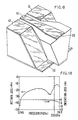
- FIG. 9 is a simplified schematic top view of top surface of the device of FIG. 8.
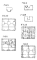
- FIG. 10 shows the layout of an array of the devices of FIG. 9 for batch fabrication on a semiconductor substrate.
- FIG. 11 shows the etched area shaded. The etch must continue all the way through the semiconductor substrate.
- any of the etches used for mesa and gate recess definiation for GaAs FET's will do if GaAs is the chosen material. Because of the slowness of the [111] surface to virtually any wet etch, the wafer should be aligned so that a "vee” will form in the vertical direction, as shown in the section 12-12 of FIG. 11 and FIG. 12. Also, a “dovetail” will form in the orthorgonal direction, as shown in the section 13-13 of FIG. 11 and FIG. 13. The “dovetail” is not necessary for the operation of the device of the invention. If anything, it complicates things. The angle ⁇ shown in FIG. 12 is approximately 55°. (See: J.Electrochemical Soc.
- FIG. 14 shows in shading the metallation patterm superimposed on the array of FIG. 11 after the etching step.
- FIG. 15 shows in dotted lines how where the array is die cut to separate individual devices either by diamond or laser scribing.
- the first mask shown in FIG. 16, is used for substrate etching using a solution of H2SO4:H2O2:H2O.
- FIG. 17 shows the second mask used for top surface metalization.
Landscapes
- Engineering & Computer Science (AREA)
- Manufacturing & Machinery (AREA)
- Internal Circuitry In Semiconductor Integrated Circuit Devices (AREA)
- Waveguides (AREA)
- Drying Of Semiconductors (AREA)
- Semiconductor Integrated Circuits (AREA)
Applications Claiming Priority (2)
| Application Number | Priority Date | Filing Date | Title |
|---|---|---|---|
| US241638 | 1981-03-09 | ||
| US07/241,638 US4906953A (en) | 1988-09-08 | 1988-09-08 | Broadband microstrip to coplanar waveguide transition by anisotropic etching of gallium arsenide |
Publications (2)
| Publication Number | Publication Date |
|---|---|
| EP0358497A2 true EP0358497A2 (de) | 1990-03-14 |
| EP0358497A3 EP0358497A3 (de) | 1991-01-16 |
Family
ID=22911538
Family Applications (1)
| Application Number | Title | Priority Date | Filing Date |
|---|---|---|---|
| EP19890309055 Ceased EP0358497A3 (de) | 1988-09-08 | 1989-09-07 | Breitbandiger Übergang von Mikrostreifenleitung auf koplanaren Wellenleiter durch anisotropes Ätzen von Galliumarsenid |
Country Status (5)
| Country | Link |
|---|---|
| US (1) | US4906953A (de) |
| EP (1) | EP0358497A3 (de) |
| JP (1) | JPH02113703A (de) |
| CA (1) | CA1323913C (de) |
| IL (1) | IL91169A (de) |
Cited By (11)
| Publication number | Priority date | Publication date | Assignee | Title |
|---|---|---|---|---|
| EP0749175A3 (de) * | 1995-06-12 | 1997-06-11 | Endgate Technology Corp | Aktive Miniaturübergang zwischen einem Mikrostreifenleiter und einem koplanaren Wellenleiter |
| US5821815A (en) * | 1996-09-25 | 1998-10-13 | Endgate Corporation | Miniature active conversion between slotline and coplanar waveguide |
| US5978666A (en) * | 1994-09-26 | 1999-11-02 | Endgate Corporation | Slotline-mounted flip chip structures |
| US5983089A (en) * | 1994-09-26 | 1999-11-09 | Endgate Corporation | Slotline-mounted flip chip |
| US6094114A (en) * | 1994-09-26 | 2000-07-25 | Endgate Corporation | Slotline-to-slotline mounted flip chip |
| US6265937B1 (en) | 1994-09-26 | 2001-07-24 | Endgate Corporation | Push-pull amplifier with dual coplanar transmission line |
| GB2381668A (en) * | 2001-11-01 | 2003-05-07 | Marconi Optical Components Ltd | Microstrip to coplanar waveguide transition |
| EP1363350A1 (de) * | 2002-05-16 | 2003-11-19 | Corning Incorporated | Breitbandiger uniplanarer Koplanarübergang |
| EP1308769A3 (de) * | 2001-11-01 | 2004-02-04 | OpNext Japan, Inc. | Optische Übertragungsvorrichtung |
| EP1467430A1 (de) * | 2003-04-11 | 2004-10-13 | TDK Corporation | Hochfrequenz-Übertragungsleitung und Hochfrequenzplatte |
| US10033080B2 (en) | 2014-05-07 | 2018-07-24 | Alcatel Lucent | Electrochromic cell for radio-frequency applications |
Families Citing this family (19)
| Publication number | Priority date | Publication date | Assignee | Title |
|---|---|---|---|---|
| US5142351A (en) * | 1989-08-31 | 1992-08-25 | Hewlett-Packard Company | Via-less two-metal tape-automated bonding system |
| US5213876A (en) * | 1990-01-11 | 1993-05-25 | Hewlett-Packard Company | Flexible circuit card with laser-contoured VIAs and machined capacitors |
| JP3058898B2 (ja) * | 1990-09-03 | 2000-07-04 | 三菱電機株式会社 | 半導体装置及びその評価方法 |
| DE4128334A1 (de) * | 1991-08-27 | 1993-03-04 | Ant Nachrichtentech | Planare mikrowellenschaltung |
| US5194833A (en) * | 1991-11-15 | 1993-03-16 | Motorola, Inc. | Airbridge compensated microwave conductors |
| US5334306A (en) * | 1991-12-11 | 1994-08-02 | At&T Bell Laboratories | Metallized paths on diamond surfaces |
| US5225797A (en) * | 1992-04-27 | 1993-07-06 | Cornell Research Foundation, Inc. | Dielectric waveguide-to-coplanar transmission line transitions |
| US5239517A (en) * | 1992-08-28 | 1993-08-24 | The United States Of America As Represented By The Secretary Of The Army | Saw transducer with coplanar waveguide transition |
| US5309122A (en) * | 1992-10-28 | 1994-05-03 | Ball Corporation | Multiple-layer microstrip assembly with inter-layer connections |
| US5631446A (en) * | 1995-06-07 | 1997-05-20 | Hughes Electronics | Microstrip flexible printed wiring board interconnect line |
| US6441697B1 (en) * | 1999-01-27 | 2002-08-27 | Kyocera America, Inc. | Ultra-low-loss feedthrough for microwave circuit package |
| FR2789232A1 (fr) * | 1999-01-28 | 2000-08-04 | Cit Alcatel | Module de circuit hyperfrequence et son dispositif de connexion a un autre module |
| JP3334680B2 (ja) * | 1999-06-03 | 2002-10-15 | 株式会社村田製作所 | 高周波回路装置および通信装置 |
| DE60035553T2 (de) * | 1999-08-11 | 2008-04-17 | Kyocera Corp. | Hochfrequenzschaltungsplatte und seine Verbindungsstruktur |
| EP1291953A4 (de) * | 2000-03-06 | 2003-05-14 | Fujitsu Ltd | Millimeterwellenmodul mit sondenkontaktstellen-struktur und millimeterwellensystem mit millimeterwellenmodulen |
| US7498523B2 (en) * | 2006-02-06 | 2009-03-03 | Efficere Inc. | Direct wire attach |
| JP4629013B2 (ja) * | 2006-09-28 | 2011-02-09 | 株式会社豊田中央研究所 | 高周波回路基板 |
| CN102306862A (zh) * | 2011-05-19 | 2012-01-04 | 南京邮电大学 | 一种宽带共面波导-双面平行双线转换接头 |
| JP2015052574A (ja) * | 2013-09-09 | 2015-03-19 | 株式会社東芝 | 高周波特性測定治具装置 |
Family Cites Families (4)
| Publication number | Priority date | Publication date | Assignee | Title |
|---|---|---|---|---|
| FR2449977A1 (fr) * | 1979-02-20 | 1980-09-19 | Thomson Csf | Dispositif de transition entre une ligne coplanaire et une ligne a rubans paralleles, et circuit hyperfrequence comportant une telle transition |
| US4543544A (en) * | 1984-01-04 | 1985-09-24 | Motorola, Inc. | LCC co-planar lead frame semiconductor IC package |
| US4600907A (en) * | 1985-03-07 | 1986-07-15 | Tektronix, Inc. | Coplanar microstrap waveguide interconnector and method of interconnection |
| US4806892A (en) * | 1987-11-09 | 1989-02-21 | Trw Inc. | Inclined RF connecting strip |
-
1988
- 1988-09-08 US US07/241,638 patent/US4906953A/en not_active Expired - Fee Related
-
1989
- 1989-08-01 IL IL9116989A patent/IL91169A/en not_active IP Right Cessation
- 1989-09-07 CA CA000610589A patent/CA1323913C/en not_active Expired - Fee Related
- 1989-09-07 EP EP19890309055 patent/EP0358497A3/de not_active Ceased
- 1989-09-08 JP JP1231819A patent/JPH02113703A/ja active Pending
Cited By (15)
| Publication number | Priority date | Publication date | Assignee | Title |
|---|---|---|---|---|
| US6265937B1 (en) | 1994-09-26 | 2001-07-24 | Endgate Corporation | Push-pull amplifier with dual coplanar transmission line |
| US5978666A (en) * | 1994-09-26 | 1999-11-02 | Endgate Corporation | Slotline-mounted flip chip structures |
| US5983089A (en) * | 1994-09-26 | 1999-11-09 | Endgate Corporation | Slotline-mounted flip chip |
| US6094114A (en) * | 1994-09-26 | 2000-07-25 | Endgate Corporation | Slotline-to-slotline mounted flip chip |
| EP0749175A3 (de) * | 1995-06-12 | 1997-06-11 | Endgate Technology Corp | Aktive Miniaturübergang zwischen einem Mikrostreifenleiter und einem koplanaren Wellenleiter |
| USRE35869E (en) * | 1995-06-12 | 1998-08-11 | Endgate Corporation | Miniature active conversion between microstrip and coplanar wave guide |
| US5821815A (en) * | 1996-09-25 | 1998-10-13 | Endgate Corporation | Miniature active conversion between slotline and coplanar waveguide |
| GB2381668A (en) * | 2001-11-01 | 2003-05-07 | Marconi Optical Components Ltd | Microstrip to coplanar waveguide transition |
| EP1308769A3 (de) * | 2001-11-01 | 2004-02-04 | OpNext Japan, Inc. | Optische Übertragungsvorrichtung |
| US6734755B2 (en) | 2002-05-16 | 2004-05-11 | Corning Incorporated | Broadband uniplanar coplanar transition |
| EP1363350A1 (de) * | 2002-05-16 | 2003-11-19 | Corning Incorporated | Breitbandiger uniplanarer Koplanarübergang |
| EP1467430A1 (de) * | 2003-04-11 | 2004-10-13 | TDK Corporation | Hochfrequenz-Übertragungsleitung und Hochfrequenzplatte |
| US7193490B2 (en) | 2003-04-11 | 2007-03-20 | Tdk Corporation | High frequency transmission line and high frequency board |
| US10033080B2 (en) | 2014-05-07 | 2018-07-24 | Alcatel Lucent | Electrochromic cell for radio-frequency applications |
| US10804587B2 (en) | 2014-05-07 | 2020-10-13 | Alcatel Lucent | Electrically controllable radio-frequency circuit element having an electrochromic material |
Also Published As
| Publication number | Publication date |
|---|---|
| US4906953A (en) | 1990-03-06 |
| EP0358497A3 (de) | 1991-01-16 |
| CA1323913C (en) | 1993-11-02 |
| IL91169A (en) | 1994-06-24 |
| IL91169A0 (en) | 1990-03-19 |
| JPH02113703A (ja) | 1990-04-25 |
Similar Documents
| Publication | Publication Date | Title |
|---|---|---|
| US4906953A (en) | Broadband microstrip to coplanar waveguide transition by anisotropic etching of gallium arsenide | |
| US5063177A (en) | Method of packaging microwave semiconductor components and integrated circuits | |
| JP3218996B2 (ja) | ミリ波導波路 | |
| Ponchak et al. | Low-loss CPW on low-resistivity Si substrates with a micromachined polyimide interface layer for RFIC interconnects | |
| US6953996B2 (en) | Low-loss coplanar waveguides and method of fabrication | |
| JP3241139B2 (ja) | フィルムキャリア信号伝送線路 | |
| US5049978A (en) | Conductively enclosed hybrid integrated circuit assembly using a silicon substrate | |
| US5583468A (en) | High frequency transition from a microstrip transmission line to an MMIC coplanar waveguide | |
| US5194833A (en) | Airbridge compensated microwave conductors | |
| US6362706B1 (en) | Cavity resonator for reducing phase noise of voltage controlled oscillator | |
| Herrick et al. | Microtechnology in the development of three-dimensional circuits | |
| EP1077502A2 (de) | RF-Übergang von MMIC auf Hohlleiter und dazugehöriges Verfahren | |
| US4833521A (en) | Means for reducing signal propagation losses in very large scale integrated circuits | |
| Meier | Two new integrated-circuit media with special advantages at millimeter wavelengths | |
| JPH01112827A (ja) | 送信機 | |
| Brown et al. | Microwave and millimeter‐wave high‐Q micromachined resonators | |
| US6778041B2 (en) | Millimeter wave module and radio apparatus | |
| Dehe et al. | Membrane-supported coplanar waveguides for MMIC and sensor application | |
| US3530407A (en) | Broadband microstrip hybrid tee | |
| US4381341A (en) | Two stage etching process for through the substrate contacts | |
| US6411182B1 (en) | Cavity resonator for reducing phase noise of voltage controlled oscillator and method for fabricating the same | |
| EP0457468A2 (de) | Integrierter elektronischer Zusammenbau mit einer Transmissionslinie | |
| Lucyszyn et al. | Terahertz multi-chip module (T-MCM) technology for the 21st Century? | |
| US3519962A (en) | Microwave transmission line | |
| JP3409767B2 (ja) | 高周波回路基板 |
Legal Events
| Date | Code | Title | Description |
|---|---|---|---|
| PUAI | Public reference made under article 153(3) epc to a published international application that has entered the european phase |
Free format text: ORIGINAL CODE: 0009012 |
|
| AK | Designated contracting states |
Kind code of ref document: A2 Designated state(s): DE FR GB IT |
|
| PUAL | Search report despatched |
Free format text: ORIGINAL CODE: 0009013 |
|
| AK | Designated contracting states |
Kind code of ref document: A3 Designated state(s): DE FR GB IT |
|
| 17P | Request for examination filed |
Effective date: 19910612 |
|
| 17Q | First examination report despatched |
Effective date: 19930416 |
|
| STAA | Information on the status of an ep patent application or granted ep patent |
Free format text: STATUS: THE APPLICATION HAS BEEN REFUSED |
|
| 18R | Application refused |
Effective date: 19931008 |