EP0358513A2 - Méthode et dispositif de détection de position - Google Patents
Méthode et dispositif de détection de position Download PDFInfo
- Publication number
- EP0358513A2 EP0358513A2 EP89309096A EP89309096A EP0358513A2 EP 0358513 A2 EP0358513 A2 EP 0358513A2 EP 89309096 A EP89309096 A EP 89309096A EP 89309096 A EP89309096 A EP 89309096A EP 0358513 A2 EP0358513 A2 EP 0358513A2
- Authority
- EP
- European Patent Office
- Prior art keywords
- light
- objects
- respect
- detecting
- positional relationship
- Prior art date
- Legal status (The legal status is an assumption and is not a legal conclusion. Google has not performed a legal analysis and makes no representation as to the accuracy of the status listed.)
- Granted
Links
Images




Classifications
-
- G—PHYSICS
- G03—PHOTOGRAPHY; CINEMATOGRAPHY; ANALOGOUS TECHNIQUES USING WAVES OTHER THAN OPTICAL WAVES; ELECTROGRAPHY; HOLOGRAPHY
- G03F—PHOTOMECHANICAL PRODUCTION OF TEXTURED OR PATTERNED SURFACES, e.g. FOR PRINTING, FOR PROCESSING OF SEMICONDUCTOR DEVICES; MATERIALS THEREFOR; ORIGINALS THEREFOR; APPARATUS SPECIALLY ADAPTED THEREFOR
- G03F9/00—Registration or positioning of originals, masks, frames, photographic sheets or textured or patterned surfaces, e.g. automatically
- G03F9/70—Registration or positioning of originals, masks, frames, photographic sheets or textured or patterned surfaces, e.g. automatically for microlithography
- G03F9/7049—Technique, e.g. interferometric
Definitions
- This invention relates generally to a position detecting method and apparatus suitably usable, for example, in a semiconductor microcircuit device manufacturing exposure apparatus for lithographically transferring a fine electronic circuit pattern formed on the surface of a first object (original) such as a mask or reticle (hereinafter simply "mask") onto the surface of a second object (workpiece) such as a wafer, for relatively positioning or aligning the mask and the wafer.
- a first object original
- a mask or reticle hereinafter simply "mask”
- the relative alignment of a mask and a wafer is one important factor in respect to ensuring improved performance.
- alignment systems employed in recent exposure apparatuses submicron alignment accuracies or more strict accuracies are required in consideration of the demand for higher degree of integration of semiconductor devices.
- alignment patterns are provided on a mask and a wafer and, by utilizing positional information obtainable from these patterns, the mask and wafer are aligned.
- the manner of executing the alignment as an example there is a method wherein the amount of relative deviation of these alignment patterns is detected on the basis of image processing.
- Another method is proposed in U.S. Patent Nos. 4,037,969 and 4,514,858 and Japanese Laid-Open Patent Application, Laid-Open No. Sho 56-157033, wherein so-called zone plates are used as alignment patterns upon which light is projected and wherein the positions of light spots formed on a predetermined plane by lights from the illuminated zone plates are detected.
- an alignment method utilizing a zone plate is relatively insensitive to any defect of an alignment pattern and therefore assures relatively high alignment accuracies, as compared with an alignment method simply using a traditional alignment pattern.
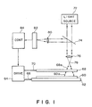
- Figure 1 is a schematic view of a known type alignment system utilizing zone plates.
- a parallel light emanating from a light source 72 passes through a half mirror 74 and is focused at a point 78 by a condensing lens 76. Thereafter, the light illuminates a mask alignment pattern 68a on a mask 68 and an alignment pattern 60a on a wafer 60 which is placed on a support table 62.
- Each of these alignment patterns 68a and 60a is provided by a reflection type zone plate and functions to form a spot of focused light on a plane perpendicular to an optical axis which contains the point 78. The amount of relative deviation of the positions of these light spots formed on that plane is detected, by directing the focused beams to a detection plane 82 by means of the condensing lens 76 and another lens 80.
- a control circuit 84 actuates a driving circuit 64 to relatively align the mask 68 and the wafer 60.
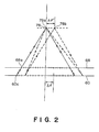
- Figure 2 illustrates an imaging relationship of lights from the mask alignment pattern 68a and the wafer alignment pattern 60a shown in Figure 1.
- a portion of the light divergently advancing from the point 78 is reflectively diffracted by the mask alignment pattern 68a and forms a spot 78a of focused light at or adjacent to the point 78, the spot representing the mask position.
- Another portion of the light passes through the mask 68 in the form of a zeroth order transmission light and is projected upon the wafer alignment pattern 60a on the wafer 60 surface with its wavefront being unchanged.
- the incident light is reflectively diffracted by the wafer alignment pattern 60a and then passes again through the mask 68 in the form of a zero-th order transmission light, and finally is focused in the neighborhood of the point 78 to form a spot 78b of focused light, representing the wafer position.
- the mask 68 functions merely as a transparent member.
- the position of the spot 78b formed by the wafer alignment pattern 60a in the described manner represents a deviation ⁇ ′, in the plane perpendicular to the optical axis containing the point 78, of an amount corresponding to the amount of deviation ⁇ of the wafer 60 with respect to the mask 68.
- Figure 3 is a schematic representation, illustrating a major part of one embodiment of the present invention.
- a light source 3 such as a semiconductor laser, for example
- the parallel light is converged by a beam reducing projection lens 5 which is used, as required, for optimizing the spot diameter to be formed on a mask 1 surface.
- the light is deflected by a deflecting mirror 6 to be projected upon a first physical optic element which is provided in a portion of the surface of a first object 1 such as a mask, for example.
- Diffraction light of a predetermined order or orders from the first physical optic element on the first object 1 is inputted to a second physical optic element which is provided in a portion of the surface of a second object 2 which is a wafer, for example.
- the inputted light is diffracted by the second physical optic element and the thus produced diffraction light is collected as a signal light by a light receiving lens 7.
- a photodetector 8 the position of the center of gravity of this signal light is detected.
- center of gravity of light means such a point that, when in the plane of light detecting surface a position vector of each point in the plane is multiplied by the light intensity of that point and the thus obtained products are integrated over the entire plane, the integrated value has a "zero vector”.
- Computing means 11 serves to compute the amount of deviation, by using a signal from the photodetector 8 and a reference signal from a memory means 12, which will be described later.
- grating lenses such as Fresnel zone plates, for example, are used as the first and second physical optic elements.
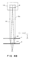
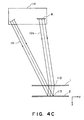
- Figures 4A and 4B schematically illustrate a path of light 111 which, in this embodiment, emanates from the light source 3 and is incident on the first object 1 and which, after being diffracted, is incident on the second object 2 and, finally, is reflectively diffracted toward a light receiving surface 8.
- what is to be detected is the amount of positional deviation between a mask (first object) 1 and a wafer (second object) 2 in the X direction.
- the light 111 from the light source 3 is projected on the surface of a first off-axis type grating element 112 (first physical optic element) provided in a portion of the mask 1, with an angle ⁇ 1 of incidence with respect to a normal to the mask 1 surface.
- Diffraction light of a predetermined order or orders from the grating element 112 emanates perpendicularly from the mask 1 and impinges on a second off-axis type grating element 113 (second physical optic element) provided in a portion of the wafer 2.
- off-axis type grating element means such an element wherein, when a light having a given angle of inclination with respect to a normal to the plane in which the element is formed is incident on the element, the property of the element is assured with respect to light of a particular order or orders other than the order of specularly reflected light or rectilinearly transmitted light.
- the first off-axis type grating element 112 in this embodiment, comprises a zone plate which is adapted to form a one-dimensional image with a light focused at a finite focal distance in the plane of the sheet of Figure 4B (i.e. the X-Z plane) but not focused in the plane of the sheet of Figure 4A (i.e. the Y-Z plane), with its chief ray extending substantially in the direction of a normal to the mask 1.
- the grating element 113 comprises, in this embodiment, a zone plate which is adapted to emit a light (with which an image is formed on the photoreceptor 8 in respect to the plane of the sheet of Figure 4B), with an angle of emission of ⁇ 2 in the sheet of Figure 4A with respect to a normal to the wafer 2, with the one-dimensional image formed by the mask 1 being taken as an object point.
- the reference 10a denotes the light flux to be received.
- the grating elements 112 and 113 can be treated each as a lens.
- the grating element 112 can serve as a concave lens while the grating element 113 can serve as a convex lens. If, in this structure, the wafer 2 shifts in the X direction, the angle of emission of the light emanating from the grading element 113 changes, as if axial alignment of a lens in an optical system is destroyed. As a result, there occurs a change in the position of incidence of the light upon the photodetector 8.
- Denoted at 114 is an optical pickup casing (alignment head) in which a light source and optical elements (not shown) for providing the light 111 to be projected as described as well as the photoreceptor 8 are accommodated.
- Denoted 115 is exposure light for transferring a pattern of the mask 1 to the wafer 2, with an illustrated chain line depicting the boundary of the path thereof. As for the exposure light, ultraviolet light, X-rays or otherwise may be used.
- the light flux 10a as depicted in Figures 4A and 4B is such light as having been diffractively transmitted through the mask 1 with a predetermined order (e.g. first order) and having been diffractively reflected by the wafer 2 with a predetermined order (e.g., first order) and finally having been transmitted through the mask 1 with zeroth order.
- a predetermined order e.g. first order
- a predetermined order e.g., first order
- first order e.g., first order
- 0-1-1 light such a light flux as having been transmitted through the mask 1 with zeroth order and having been diffractively reflected by the wafer 1 with first order and finally having been diffractively transmitted through the mask 1 with first order
- 0-1-1 light can form a spot on the photoreceptor 8 surface in the neighborhood of a spot provided by the 1-1-0 light.
- the 0-1-1 light can cause shift of the position of incidence on the detector 8 as a result of the shift of the wafer 2.
- each of deviations ⁇ 110 and ⁇ 011 of respective gravity centers of the 1-1-0 light and the 0-1-1 light, upon the detecting surface 8, is substantially in a linear relationship with the deviation ⁇ , because of a paraxial imaging magnification as determined by the refracting power arrangement of the system provided by the two grating elements 112 and 113.
- what is detected may be the position of center of gravity of combined two spots whose positions are changeable at different magnifications with a positional deviation ⁇ between the mask and the wafer.
- Any change in the position of this center of gravity, to be detected is substantially in a linear relationship with the mask-to-wafer deviation ⁇ and, therefore, by predetecting a proportional constant of the same, it is possible to determine the deviation ⁇ on the basis of the shift of the position of the center of gravity.
- trial printing may be made to determine, as a reference position, the position of the center of gravity to be defined when the mask and the wafer do not include any positional deviation.
- the amount of positional deviation of the center of gravity from the reference position in the X direction may be detected to determine the amount of relative deviation of the mask and the wafer, on the basis of the aforementioned proportional relationship.
- the relationship of the deviations ⁇ y, ⁇ x and ⁇ is memorized in preparation into a storing means 12 (as will be described later). Making reference to a signal from such storing means 12, it is possible to attain high-precision alignment in the alignment direction under the influence of the computing means 11.
- alignment marks are provided at four sites around an exposure area, for detection of two-dimensional positional deviation (lateral shift and rotational error) between a first object (such as a mask) and a second object (such as a wafer).
- An example is schematically illustrated in Figure 3.
- alignment marks are provided in four regions A - D which are on a scribe line 20 surrounding an exposure area 10.
- Each of these alignment marks may comprise an off-axis type grating element as described hereinbefore.
- those optical systems such as shown in Figure 3 may be used.
- any deviation in the X direction is detected while, on the other hand, with regard to the regions C and D any deviation in the Y direction is detected.
- Figure 5 is an explanatory representation, illustrating the relationship between (i) a positional deviation ⁇ x of the mask and wafer in the alignment direction (X direction) in respect to the regions A and B shown in Figure 3 and (ii) a deviation ⁇ of the center of gravity of a spot on the detecting surface, from a reference position.
- the illustrated corresponds to a case where the refracting power and arrangement of the grating element (physical optic element) are set so that the deviation ⁇ is in a ratio of about 100 to the deviation ⁇ x.
- the relationship therebetween is slightly non-linear because of the aberration of the grating element, for example, this raises substantially no problem in regard to the precision of position detection.
- the deviation ⁇ corresponds, in principle, to the deviation ⁇ x in the alignment direction (X direction). Actually, however, for the reasons described hereinbefore, it can be affected by a positional deviation ⁇ y in a direction (Y direction) perpendicular to the alignment direction.
- any error resulting from the positional deviation in the direction (Y direction) perpendicular to the alignment direction is corrected.
- the proportional constant in regard to the proportional relationship used for calculation of ⁇ x from the deviation ⁇ may be changed.
- the precision for detecting the positional deviation ⁇ y it may be relatively low. As an example, in Figure 5, if the deviation ⁇ y can be detected with a precision of ⁇ 1 micron, then the precision of detecting the deviation ⁇ x (where it is in a range of ⁇ 3 microns) can be enhanced to about ⁇ 0.01 micron.
- Figure 6 exemplifies the flow of sequence for detecting lateral deviations ⁇ X and ⁇ Y of a mask and a wafer in the X and Y directions as well as a rotational error ⁇ therebetween, by using the computing means 11 and in accordance with the method described hereinbefore. Details of the sequential operations will now be explained.
- the detecting method is not limited to the disclosed one, and various methods can be used with the present invention.
Landscapes
- Physics & Mathematics (AREA)
- General Physics & Mathematics (AREA)
- Exposure And Positioning Against Photoresist Photosensitive Materials (AREA)
- Length Measuring Devices By Optical Means (AREA)
- Exposure Of Semiconductors, Excluding Electron Or Ion Beam Exposure (AREA)
Applications Claiming Priority (6)
| Application Number | Priority Date | Filing Date | Title |
|---|---|---|---|
| JP22580388 | 1988-09-09 | ||
| JP22580388 | 1988-09-09 | ||
| JP225803/88 | 1988-09-09 | ||
| JP209924/89 | 1989-08-14 | ||
| JP1209924A JP2626076B2 (ja) | 1988-09-09 | 1989-08-14 | 位置検出装置 |
| JP20992489 | 1989-08-14 |
Publications (3)
| Publication Number | Publication Date |
|---|---|
| EP0358513A2 true EP0358513A2 (fr) | 1990-03-14 |
| EP0358513A3 EP0358513A3 (fr) | 1991-01-02 |
| EP0358513B1 EP0358513B1 (fr) | 2000-05-10 |
Family
ID=26517751
Family Applications (1)
| Application Number | Title | Priority Date | Filing Date |
|---|---|---|---|
| EP89309096A Expired - Lifetime EP0358513B1 (fr) | 1988-09-09 | 1989-09-07 | Méthode et dispositif de détection de position |
Country Status (4)
| Country | Link |
|---|---|
| US (1) | US5148035A (fr) |
| EP (1) | EP0358513B1 (fr) |
| JP (1) | JP2626076B2 (fr) |
| DE (1) | DE68929205T2 (fr) |
Cited By (1)
| Publication number | Priority date | Publication date | Assignee | Title |
|---|---|---|---|---|
| US5377009A (en) * | 1991-01-11 | 1994-12-27 | Canon Kabushiki Kaisha | Alignment method |
Families Citing this family (3)
| Publication number | Priority date | Publication date | Assignee | Title |
|---|---|---|---|---|
| US5455679A (en) * | 1993-02-22 | 1995-10-03 | Canon Kabushiki Kaisha | Position detecting system |
| US20040237637A1 (en) * | 2003-01-17 | 2004-12-02 | Andre Veinotte | Flow sensor for purge valve diagnostic |
| JP5032156B2 (ja) * | 2007-03-05 | 2012-09-26 | ジーイー・メディカル・システムズ・グローバル・テクノロジー・カンパニー・エルエルシー | 磁気共鳴イメージング装置および磁気共鳴イメージング方法 |
Family Cites Families (15)
| Publication number | Priority date | Publication date | Assignee | Title |
|---|---|---|---|---|
| US4037969A (en) * | 1976-04-02 | 1977-07-26 | Bell Telephone Laboratories, Incorporated | Zone plate alignment marks |
| US4360273A (en) * | 1980-02-14 | 1982-11-23 | Sperry Corporation | Optical alignment of masks for X-ray lithography |
| US4326805A (en) * | 1980-04-11 | 1982-04-27 | Bell Telephone Laboratories, Incorporated | Method and apparatus for aligning mask and wafer members |
| US4539482A (en) * | 1980-10-09 | 1985-09-03 | Canon Kabushiki Kaisha | Reading apparatus |
| US4398824A (en) * | 1981-04-15 | 1983-08-16 | Bell Telephone Laboratories, Incorporated | Wafer tilt compensation in zone plate alignment system |
| US4636626A (en) * | 1983-01-14 | 1987-01-13 | Nippon Kogaku K.K. | Apparatus for aligning mask and wafer used in semiconductor circuit element fabrication |
| US4545683A (en) * | 1983-02-28 | 1985-10-08 | The Perkin-Elmer Corporation | Wafer alignment device |
| US4514858A (en) * | 1983-03-15 | 1985-04-30 | Micronix Partners | Lithography system |
| US4656347A (en) * | 1984-01-30 | 1987-04-07 | Nippon Telegraph & Telephone Public Corporation | Diffraction grating position adjuster using a grating and a reflector |
| JPS60163110A (ja) * | 1984-02-06 | 1985-08-26 | Canon Inc | 位置合わせ装置 |
| US4701050A (en) * | 1984-08-10 | 1987-10-20 | Hitachi, Ltd. | Semiconductor exposure apparatus and alignment method therefor |
| JPS61111402A (ja) * | 1984-11-06 | 1986-05-29 | Nippon Kogaku Kk <Nikon> | 位置検出装置 |
| US4812661A (en) * | 1986-08-20 | 1989-03-14 | Hewlett-Packard Company | Method and apparatus for hybrid I.C. lithography |
| JPS63131008A (ja) * | 1986-11-20 | 1988-06-03 | Fujitsu Ltd | 光学的アライメント方法 |
| DE3853246T2 (de) * | 1987-09-25 | 1995-06-29 | Matsushita Electric Industrial Co., Ltd., Kadoma, Osaka | Vorrichtung zur Kontrolle des Lageverhältnisses zwischen einer Photomaske und einem Plättchen. |
-
1989
- 1989-08-14 JP JP1209924A patent/JP2626076B2/ja not_active Expired - Fee Related
- 1989-09-07 DE DE68929205T patent/DE68929205T2/de not_active Expired - Fee Related
- 1989-09-07 EP EP89309096A patent/EP0358513B1/fr not_active Expired - Lifetime
-
1991
- 1991-11-12 US US07/789,630 patent/US5148035A/en not_active Expired - Fee Related
Cited By (1)
| Publication number | Priority date | Publication date | Assignee | Title |
|---|---|---|---|---|
| US5377009A (en) * | 1991-01-11 | 1994-12-27 | Canon Kabushiki Kaisha | Alignment method |
Also Published As
| Publication number | Publication date |
|---|---|
| JPH02167405A (ja) | 1990-06-27 |
| DE68929205D1 (de) | 2000-06-15 |
| US5148035A (en) | 1992-09-15 |
| JP2626076B2 (ja) | 1997-07-02 |
| DE68929205T2 (de) | 2000-09-28 |
| EP0358513A3 (fr) | 1991-01-02 |
| EP0358513B1 (fr) | 2000-05-10 |
Similar Documents
| Publication | Publication Date | Title |
|---|---|---|
| JP3570728B2 (ja) | 離軸整列ユニットを持つリトグラフ投射装置 | |
| US5148037A (en) | Position detecting method and apparatus | |
| EP0409572B1 (fr) | Système de détection de position | |
| EP0329430B1 (fr) | Dispositif de détection de position | |
| EP0411966A2 (fr) | Méthode et dispositif de détection de position | |
| US5396335A (en) | Position detecting method | |
| US5235408A (en) | Position detecting method and apparatus | |
| US5225892A (en) | Positional deviation detecting method | |
| US5495336A (en) | Position detecting method for detecting a positional relationship between a first object and a second object | |
| US5319444A (en) | Position detecting method and apparatus | |
| US5481363A (en) | Positional deviation detecting method | |
| JP3428705B2 (ja) | 位置検出装置及びそれを用いた半導体素子の製造方法 | |
| EP0358425A2 (fr) | Méthode et dispositif de détection de position | |
| US5294980A (en) | Positioning detecting method and apparatus | |
| JP2650396B2 (ja) | 位置検出装置及び位置検出方法 | |
| JP3368017B2 (ja) | 位置検出装置及びそれを用いた半導体素子の製造方法 | |
| EP0358513B1 (fr) | Méthode et dispositif de détection de position | |
| US5455679A (en) | Position detecting system | |
| EP0333326B1 (fr) | Procédé et dispositif pour détecter la position | |
| US4701050A (en) | Semiconductor exposure apparatus and alignment method therefor | |
| EP0358511B1 (fr) | Dispositif de détection de la relation de position de deux objets | |
| KR0160544B1 (ko) | 웨이퍼 스텝퍼에서 정렬광의 경사조명에 의한 웨이퍼 정렬방법과 그 장치 | |
| EP0441578B1 (fr) | Méthode pour la détection des écarts de position | |
| JP2615778B2 (ja) | 位置合わせ装置 | |
| JPH01209721A (ja) | 投影露光装置 |
Legal Events
| Date | Code | Title | Description |
|---|---|---|---|
| PUAI | Public reference made under article 153(3) epc to a published international application that has entered the european phase |
Free format text: ORIGINAL CODE: 0009012 |
|
| AK | Designated contracting states |
Kind code of ref document: A2 Designated state(s): DE FR GB NL |
|
| PUAL | Search report despatched |
Free format text: ORIGINAL CODE: 0009013 |
|
| AK | Designated contracting states |
Kind code of ref document: A3 Designated state(s): DE FR GB NL |
|
| 17P | Request for examination filed |
Effective date: 19901231 |
|
| 17Q | First examination report despatched |
Effective date: 19930528 |
|
| GRAG | Despatch of communication of intention to grant |
Free format text: ORIGINAL CODE: EPIDOS AGRA |
|
| GRAG | Despatch of communication of intention to grant |
Free format text: ORIGINAL CODE: EPIDOS AGRA |
|
| GRAH | Despatch of communication of intention to grant a patent |
Free format text: ORIGINAL CODE: EPIDOS IGRA |
|
| GRAH | Despatch of communication of intention to grant a patent |
Free format text: ORIGINAL CODE: EPIDOS IGRA |
|
| GRAA | (expected) grant |
Free format text: ORIGINAL CODE: 0009210 |
|
| AK | Designated contracting states |
Kind code of ref document: B1 Designated state(s): DE FR GB NL |
|
| REF | Corresponds to: |
Ref document number: 68929205 Country of ref document: DE Date of ref document: 20000615 |
|
| ET | Fr: translation filed | ||
| PLBE | No opposition filed within time limit |
Free format text: ORIGINAL CODE: 0009261 |
|
| STAA | Information on the status of an ep patent application or granted ep patent |
Free format text: STATUS: NO OPPOSITION FILED WITHIN TIME LIMIT |
|
| 26N | No opposition filed | ||
| REG | Reference to a national code |
Ref country code: GB Ref legal event code: IF02 |
|
| PGFP | Annual fee paid to national office [announced via postgrant information from national office to epo] |
Ref country code: GB Payment date: 20030826 Year of fee payment: 15 |
|
| PGFP | Annual fee paid to national office [announced via postgrant information from national office to epo] |
Ref country code: FR Payment date: 20030919 Year of fee payment: 15 Ref country code: DE Payment date: 20030919 Year of fee payment: 15 |
|
| PGFP | Annual fee paid to national office [announced via postgrant information from national office to epo] |
Ref country code: NL Payment date: 20030930 Year of fee payment: 15 |
|
| PG25 | Lapsed in a contracting state [announced via postgrant information from national office to epo] |
Ref country code: GB Free format text: LAPSE BECAUSE OF NON-PAYMENT OF DUE FEES Effective date: 20040907 |
|
| PG25 | Lapsed in a contracting state [announced via postgrant information from national office to epo] |
Ref country code: NL Free format text: LAPSE BECAUSE OF NON-PAYMENT OF DUE FEES Effective date: 20050401 Ref country code: DE Free format text: LAPSE BECAUSE OF NON-PAYMENT OF DUE FEES Effective date: 20050401 |
|
| GBPC | Gb: european patent ceased through non-payment of renewal fee |
Effective date: 20040907 |
|
| PG25 | Lapsed in a contracting state [announced via postgrant information from national office to epo] |
Ref country code: FR Free format text: LAPSE BECAUSE OF NON-PAYMENT OF DUE FEES Effective date: 20050531 |
|
| NLV4 | Nl: lapsed or anulled due to non-payment of the annual fee |
Effective date: 20050401 |
|
| REG | Reference to a national code |
Ref country code: FR Ref legal event code: ST |