EP0360176B2 - Optisches Wellenleitermodul mit Faserankopplung - Google Patents
Optisches Wellenleitermodul mit Faserankopplung Download PDFInfo
- Publication number
- EP0360176B2 EP0360176B2 EP89117163A EP89117163A EP0360176B2 EP 0360176 B2 EP0360176 B2 EP 0360176B2 EP 89117163 A EP89117163 A EP 89117163A EP 89117163 A EP89117163 A EP 89117163A EP 0360176 B2 EP0360176 B2 EP 0360176B2
- Authority
- EP
- European Patent Office
- Prior art keywords
- fiber
- supporting bodies
- substrate
- optical waveguide
- optical
- Prior art date
- Legal status (The legal status is an assumption and is not a legal conclusion. Google has not performed a legal analysis and makes no representation as to the accuracy of the status listed.)
- Expired - Lifetime
Links
- 239000000835 fiber Substances 0.000 title claims description 41
- 230000008878 coupling Effects 0.000 title claims description 21
- 238000010168 coupling process Methods 0.000 title claims description 21
- 238000005859 coupling reaction Methods 0.000 title claims description 21
- 230000003287 optical effect Effects 0.000 title claims description 14
- 239000000758 substrate Substances 0.000 claims description 17
- 239000013307 optical fiber Substances 0.000 claims description 7
- VYPSYNLAJGMNEJ-UHFFFAOYSA-N Silicium dioxide Chemical compound O=[Si]=O VYPSYNLAJGMNEJ-UHFFFAOYSA-N 0.000 claims description 5
- 239000000853 adhesive Substances 0.000 claims description 2
- 230000001070 adhesive effect Effects 0.000 claims description 2
- XUIMIQQOPSSXEZ-UHFFFAOYSA-N Silicon Chemical compound [Si] XUIMIQQOPSSXEZ-UHFFFAOYSA-N 0.000 description 4
- 229910052710 silicon Inorganic materials 0.000 description 4
- 239000010703 silicon Substances 0.000 description 4
- 238000005516 engineering process Methods 0.000 description 3
- 238000004519 manufacturing process Methods 0.000 description 3
- 239000011521 glass Substances 0.000 description 2
- 239000003365 glass fiber Substances 0.000 description 2
- 239000000463 material Substances 0.000 description 2
- 230000010287 polarization Effects 0.000 description 2
- 230000002787 reinforcement Effects 0.000 description 2
- 230000005540 biological transmission Effects 0.000 description 1
- 239000011248 coating agent Substances 0.000 description 1
- 238000000576 coating method Methods 0.000 description 1
- 238000004891 communication Methods 0.000 description 1
- 230000007613 environmental effect Effects 0.000 description 1
- 238000005530 etching Methods 0.000 description 1
- 239000003292 glue Substances 0.000 description 1
- GQYHUHYESMUTHG-UHFFFAOYSA-N lithium niobate Chemical compound [Li+].[O-][Nb](=O)=O GQYHUHYESMUTHG-UHFFFAOYSA-N 0.000 description 1
- 229910052751 metal Inorganic materials 0.000 description 1
- 239000002184 metal Substances 0.000 description 1
- 238000000465 moulding Methods 0.000 description 1
- 239000007858 starting material Substances 0.000 description 1
- 239000004575 stone Substances 0.000 description 1
Images
Classifications
-
- G—PHYSICS
- G02—OPTICS
- G02B—OPTICAL ELEMENTS, SYSTEMS OR APPARATUS
- G02B6/00—Light guides; Structural details of arrangements comprising light guides and other optical elements, e.g. couplings
- G02B6/24—Coupling light guides
- G02B6/42—Coupling light guides with opto-electronic elements
- G02B6/4201—Packages, e.g. shape, construction, internal or external details
- G02B6/4204—Packages, e.g. shape, construction, internal or external details the coupling comprising intermediate optical elements, e.g. lenses, holograms
- G02B6/4212—Packages, e.g. shape, construction, internal or external details the coupling comprising intermediate optical elements, e.g. lenses, holograms the intermediate optical element being a coupling medium interposed therebetween, e.g. epoxy resin, refractive index matching material, index grease, matching liquid or gel
-
- G—PHYSICS
- G02—OPTICS
- G02B—OPTICAL ELEMENTS, SYSTEMS OR APPARATUS
- G02B6/00—Light guides; Structural details of arrangements comprising light guides and other optical elements, e.g. couplings
- G02B6/24—Coupling light guides
- G02B6/26—Optical coupling means
- G02B6/30—Optical coupling means for use between fibre and thin-film device
Definitions
- the invention relates to an optical waveguide module the closer in the preamble of claim 1 designated execution.
- Such modules are known for example from GB-A-2 184 255 and are generally used as sensors and for optical communication technology and sensor technology used. They exist from planar structures, in which a carrier substrate with integrated optical circuit e.g. as Phase modulator, beam splitter, Mach-Zehnder interferometer etc. is realized.
- a carrier substrate with integrated optical circuit e.g. as Phase modulator, beam splitter, Mach-Zehnder interferometer etc. is realized.
- the fiber ends are fixed between a grooved silicon plate and a glass plate covering the grooves, and the arrangement is glued to the outside of the carrier substrate, which is again mechanically reinforced by means of a strip in the connection region.
- the fiber coupling designed for the group connection of glass fibers is relatively expensive to manufacture and less suitable for coupling individual fibers.
- the groove in the silicon wafer is produced by anisotropic etching, which is relatively time-consuming.
- silicon is quite fragile due to its crystalline structure, therefore requires special care in handling and requires mechanical reinforcement by the glass plate to increase stability.
- the fiber coupling in groups requires very good centering of the fiber core with respect to the fiber jacket. In particular, polarization-maintaining fibers for wavelengths ⁇ 1 ⁇ m are not able to meet these conditions.
- the invention is based on the object an optical waveguide module at the beginning explained the optical transmission properties to improve fiber coupling.
- This Task is inventively by the in Design measures specified solved.
- Refinements of the fiber coupling of the Waveguide module are to the subclaims remove. Advantages achievable with the invention are mentioned in the description.
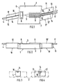
- 1 to 4 is the waveguide module called the following module for short - generally with 1 designated. It essentially consists of one Substrate carrier 2 with at least one integrated Optical fiber 3, at the ends of each an optical Fiber connecting line 4, 5, 5 'is coupled. Depending on the intended use and location, this is Module 1 mechanically protected in a housing housed that depending on possible Environmental influences must be sealed gas-tight can (not shown).
- Module 1 In the present embodiment of the Module 1 is the waveguide 3 as a beam splitter Y branch formed, which on the coupling side 6 of module 1 begins on one Auskoppelseite 7 ends with two lanes and one integrated polarizer 8 and an integrated Phase modulator 9 happens.
- the fiber couplings 10, 11, 11 'on the Einund Decoupling side 6, 7 of module 1 exist each made of a strip-shaped carrier body 12, 13, 13 'with a cut on the top and extending in the direction of the longitudinal axis Groove 14.
- each groove 14 is one of the outer Wrapping and the primary coating exempted fiber end 15 of the corresponding connecting line 4, 5, 5 'fixed with glue.
- At the fiber ends 15 acts e.g. about polarization-maintaining monomode fibers made of quartz glass, for example a Have a jacket diameter of 85 ⁇ m.
- the width of the groove 14 in the carrier body 12, 13, 13 ' e.g. 100 ⁇ m and the depth to completely recessed intake of the fiber end 15 and a sufficient amount of adhesive 150 ⁇ m up to 200 ⁇ m.
- the carrier bodies are advantageously made of commercially available quartz glass substrates Quality manufactured that is in contrast to silicon have it polished well. Have these substrates Dimensions of 50x50x1 mm from which e.g. 1 mm wide, 1 mm thick and 4 mm long strips cut and grooved. At the present embodiment have the Carrier body 12, 13, 13 'has a square cross section on. However, you can also use a rectangular one Have cross-section; the grooves 14 are then arranged on one of the narrow long sides. To unwanted back reflections from light waves to avoid the end faces of the vitreous at a predetermined angle to the fiber axis be arranged depending on the Waveguide longitudinal axis of the substrate carrier 2 angular arranged coupling and decoupling sides 6, 7 is determined.
- the carrier bodies 13, 13 'contain grooves 14 which parallel at a small distance next to an outer edge extend on the outer edges of the long sides facing each other in the installed position the carrier body.
- the distance of the grooves 14 from one another depends on that of the optical waveguide 3 of the substrate carrier 2, which here, for example Is 450 ⁇ m. Therefore, with the support bodies 13, 13 'a groove distance of about 50 microns to the outer edge sufficient for individual adjustment the fiber ends 15 on the corresponding Optical fiber output and subsequent fixing to ensure the carrier body 13, 13 ', although the arrangement at even smaller intervals such as. 20 ⁇ m is possible.
- the carrier body 12 13, 13 'is a starting material chosen the one the fiber end 15 of the Fiber connection line 4, 5, 5 'adapted expansion coefficient has, so if possible from the the same material as the fiber end.
- the end faces of support bodies and embedded fiber ends polished together which gives them a relatively large flat surface with which they are mechanically stable and stress-free the correspondingly polished sides of the substrate carrier 2 are glued.
- the ones described can Carrier body also for mounting and coupling from other optical fibers, e.g. Multimode, or other single-mode fibers Quartz glass can be used.
Landscapes
- Physics & Mathematics (AREA)
- General Physics & Mathematics (AREA)
- Optics & Photonics (AREA)
- Optical Couplings Of Light Guides (AREA)
- Optical Integrated Circuits (AREA)
Description
- Fig. 1
- ein optisches Wellenleitermodul mit Faserankopplung, in der Draufsicht;
- Fig. 2
- das Wellenleitermodui der Fig. 1, in einer Seitenansicht;
- Fig. 3
- das schematisch dargestellte Wellenleitermodul der Fig. 1, mit Blick auf die Einkoppelseite der Faserankopplung:
- Fig. 4
- das schematisch dargestellte Wellenleitermodul der Fig. 1, mit Blick auf die Auskoppelseite der Faserankopplung.
Claims (3)
- Optisches Wellenleitermodul (1) in IOC-Bauweise mit Faserankopplung (10, 11, 11'), das aus einem Trägersubstrat (2) mit wenigstens einem Lichtwellenleiter (3) besteht, dessen Enden auf zwei Seiten des Trägersubstrates (2) an je eine optische Anschlußleitung (4, 5, 5') gekoppelt sind, wobei die Anchlußleitungen (4, 5, 5') mit vom Primärcoating befreiten Faserenden (15) in je einer Nut (14) einer separaten, bezüglich des Trägersubstrates (2) justierten und daran befestigten, aus je einem leistenförmigen Trägerkörper (12, 13, 13') bestehenden Halterung mit einem Kleber fixiert sind,
dadurch gekennzeichnet, daß die Nuten (14) aufderOberseitein Richtung der Längsachse der Trägerkörper (12, 13, 13') eingeschnitten sind und daß die Faserenden (15) und die leistenförmigen Trägerkörper (12, 13, 13') aus Quarzglas mit einem einander angepaßten Ausdehnungskoeffizienten bestehen. - Optisches Wellenleitermodul (1) nach Anspruch 1, dadurch gekennzeichnet, daß bei zwei dicht nebeneinander endenden Lichtwellenleitern (3) des Trägersubstrates (2) zwei, den Enden der Lichtwellenleiter zugeordnete Trägerkörper vorhanden sind, und daß die Nuten (14) der Trägerkörper (13, 13') sich jeweils auf der Oberseite in einem geringen Abstand von ca. 50 µm oder kleiner parallel neben der Außenkante der einander zugekehrten Längsseiten der Trägerkörper (13, 13') erstrecken.
- Optisches Wellenleitermodul (1) nach Anspruch 1 oder 2, dadurch gekennzeichnet, daß die Stirnseiten der Trägerkörper (12, 13, 13') zur Vermeidung von Rückreflexionen in je einem vorgegebenen Winkel zur Faserachse (Faserende 15) angeordnet sind.
Applications Claiming Priority (2)
| Application Number | Priority Date | Filing Date | Title |
|---|---|---|---|
| DE3831905 | 1988-09-20 | ||
| DE3831905A DE3831905A1 (de) | 1988-09-20 | 1988-09-20 | Optisches wellenleitermodul mit faserankopplung |
Publications (4)
| Publication Number | Publication Date |
|---|---|
| EP0360176A2 EP0360176A2 (de) | 1990-03-28 |
| EP0360176A3 EP0360176A3 (en) | 1990-12-19 |
| EP0360176B1 EP0360176B1 (de) | 1994-08-10 |
| EP0360176B2 true EP0360176B2 (de) | 2001-08-08 |
Family
ID=6363324
Family Applications (1)
| Application Number | Title | Priority Date | Filing Date |
|---|---|---|---|
| EP89117163A Expired - Lifetime EP0360176B2 (de) | 1988-09-20 | 1989-09-16 | Optisches Wellenleitermodul mit Faserankopplung |
Country Status (5)
| Country | Link |
|---|---|
| US (1) | US4953936A (de) |
| EP (1) | EP0360176B2 (de) |
| JP (1) | JP2533198B2 (de) |
| CA (1) | CA1315138C (de) |
| DE (2) | DE3831905A1 (de) |
Families Citing this family (16)
| Publication number | Priority date | Publication date | Assignee | Title |
|---|---|---|---|---|
| DE4012747A1 (de) * | 1990-04-21 | 1991-10-24 | Bodenseewerk Geraetetech | Verfahren zur herstellung von feinoptischen stirnflaechen an wellenleitern |
| US5095513A (en) * | 1990-11-29 | 1992-03-10 | Bodyscan Medical Corporation | Low voltage optical light modulator |
| FR2674033B1 (fr) * | 1991-03-14 | 1993-07-23 | Corning Inc | Composant optique integre a liaison entre un guide d'onde integre et une fibre optique, fonctionnant dans un large domaine de temperature. |
| DE4134940A1 (de) * | 1991-10-23 | 1993-04-29 | Bosch Gmbh Robert | Integriertes optisches bauelement sowie verfahren zu seiner herstellung |
| DE4210331A1 (de) * | 1992-03-30 | 1993-10-07 | Bodenseewerk Geraetetech | Verbindung einer Fotodiode mit einem Lichtwellenleiter |
| CA2127861C (en) * | 1993-07-14 | 2004-09-21 | Shinji Ishikawa | Coupling structure of optical fibers and optical waveguides |
| JPH0792342A (ja) * | 1993-07-29 | 1995-04-07 | Sumitomo Electric Ind Ltd | 光導波路モジュール |
| EP0652451B1 (de) * | 1993-11-08 | 2001-08-08 | Corning Incorporated | Kopplung von planaren optischen Wellenleitern und optischen Fasern mit geringer Rückreflexion |
| FR2716012B1 (fr) * | 1994-02-09 | 1996-04-12 | Corning Inc | Procédé et dispositif d'assemblage d'extrémités de fibres optiques disposées en nappe. |
| US5646674A (en) * | 1994-04-29 | 1997-07-08 | Eastman Kodak Company | Optical print head with flexure mounted optical device |
| US5471552A (en) * | 1995-02-22 | 1995-11-28 | Industrial Technology Research Institute | Fabrication of static-alignment fiber-guiding grooves for planar lightwave circuits |
| US6487341B1 (en) * | 2000-10-13 | 2002-11-26 | Agere Systems Guardian Corp | Multi-material structure with reduced polarization dependent loss and method therefor |
| JP2004054181A (ja) * | 2002-07-24 | 2004-02-19 | Fujitsu Media Device Kk | 波長フィルタ、可変波長フィルタ、及び光学素子 |
| US7257295B2 (en) * | 2004-09-20 | 2007-08-14 | Fujitsu Limited | Attachment-type optical coupler apparatuses |
| RU2280882C2 (ru) * | 2004-10-04 | 2006-07-27 | Открытое акционерное общество "Пермская научно-производственная приборостроительная компания" | Способ стыковки интегрально-оптической схемы для волоконно-оптического гироскопа с одномодовыми световодами (варианты) |
| US7555176B2 (en) * | 2007-08-22 | 2009-06-30 | Ccs Technology, Inc. | Method for producing an optical splitter, and optical splitter |
Family Cites Families (20)
| Publication number | Priority date | Publication date | Assignee | Title |
|---|---|---|---|---|
| US3864019A (en) * | 1973-11-15 | 1975-02-04 | Bell Telephone Labor Inc | Optical film-fiber coupler |
| US4186409A (en) * | 1978-08-11 | 1980-01-29 | Westinghouse Electric Corp. | Light activated silicon switch |
| JPS59146004A (ja) * | 1983-02-08 | 1984-08-21 | Sumitomo Electric Ind Ltd | 光集積回路 |
| DE3408783A1 (de) * | 1983-08-03 | 1985-02-14 | Siemens AG, 1000 Berlin und 8000 München | Verbindungselement fuer lichtwellenleiter und verfahren zur herstellung |
| DE3345715A1 (de) * | 1983-12-17 | 1985-06-27 | Philips Patentverwaltung Gmbh, 2000 Hamburg | Integriert-optisches bauelement |
| FR2574950B1 (fr) * | 1984-12-18 | 1987-09-25 | Corning Glass Works | Composants optiques integres en verre et leur fabrication |
| GB2184255B (en) * | 1985-12-13 | 1989-01-05 | Stc Plc | Optical fibre integrated optical device coupler |
| DE3605966A1 (de) * | 1986-02-25 | 1987-08-27 | Philips Patentverwaltung | Vorrichtung zum verbinden von lichtwellenleitern und verfahren zu deren herstellung |
| DE3608018A1 (de) * | 1986-03-11 | 1987-09-17 | Siemens Ag | Verbindungselement fuer mit kleber gehaltene lichtwellenleiter und verfahren zu dessen herstellung |
| US4759595A (en) * | 1986-03-25 | 1988-07-26 | Apa Optics, Inc. | Integrated optic switch |
| JPS6341807A (ja) * | 1986-08-07 | 1988-02-23 | Fujitsu Ltd | 光フアイバと光導波路との接続方法 |
| JPS6370808A (ja) * | 1986-09-12 | 1988-03-31 | Fujitsu Ltd | 導波路と光フアイバの接続方法 |
| JP2509582B2 (ja) * | 1986-10-17 | 1996-06-19 | 株式会社東芝 | 光フアイバコリメ−タ |
| US4750800A (en) * | 1986-11-04 | 1988-06-14 | United Technologies Corporation | Low stress mounting of integrated optic chips |
| FR2608785B1 (fr) * | 1986-12-19 | 1989-08-04 | Thomson Csf | Dispositif de connexion de fibres optiques a un circuit optique integre et procede de realisation |
| JP2512927B2 (ja) * | 1987-01-27 | 1996-07-03 | 日本電気株式会社 | 光導波路と光ファイバの結合構造 |
| FR2612301B1 (fr) * | 1987-03-12 | 1991-08-23 | Corning Glass Works | Composant optique integre et sa fabrication |
| US4796975A (en) * | 1987-05-14 | 1989-01-10 | Amphenol Corporation | Method of aligning and attaching optical fibers to substrate optical waveguides and substrate optical waveguide having fibers attached thereto |
| US4871226A (en) * | 1987-10-01 | 1989-10-03 | United Technologies Corporation | Mounting of optical fibers to integrated optical chips |
| FR2623915B1 (fr) * | 1987-11-26 | 1990-04-13 | Corning Glass Works | Procede de production d'un composant optique integre en verre comprenant des tranchees de positionnement et de fixation de fibres optiques en alignement avec des guides d'ondes et composants ainsi produits |
-
1988
- 1988-09-20 DE DE3831905A patent/DE3831905A1/de not_active Withdrawn
-
1989
- 1989-09-01 US US07/401,937 patent/US4953936A/en not_active Expired - Lifetime
- 1989-09-05 CA CA000610300A patent/CA1315138C/en not_active Expired - Fee Related
- 1989-09-16 DE DE58908174T patent/DE58908174D1/de not_active Expired - Fee Related
- 1989-09-16 EP EP89117163A patent/EP0360176B2/de not_active Expired - Lifetime
- 1989-09-20 JP JP1242363A patent/JP2533198B2/ja not_active Expired - Fee Related
Also Published As
| Publication number | Publication date |
|---|---|
| JP2533198B2 (ja) | 1996-09-11 |
| US4953936A (en) | 1990-09-04 |
| CA1315138C (en) | 1993-03-30 |
| EP0360176A2 (de) | 1990-03-28 |
| DE3831905A1 (de) | 1990-03-22 |
| JPH02115808A (ja) | 1990-04-27 |
| EP0360176A3 (en) | 1990-12-19 |
| DE58908174D1 (de) | 1994-09-15 |
| EP0360176B1 (de) | 1994-08-10 |
Similar Documents
| Publication | Publication Date | Title |
|---|---|---|
| EP0360176B1 (de) | Optisches Wellenleitermodul mit Faserankopplung | |
| DE3853659T2 (de) | Verbindung von optischen Fasern mit integrierten optischen Schaltungen. | |
| DE3877597T2 (de) | Verbindung von optischen fasern. | |
| DE69428558T2 (de) | Kopplungsstruktur für optische Fasern und optische Wellenleiter | |
| DE69318293T2 (de) | Selbstausrichtender flexibler optischer koppler | |
| DE68922451T2 (de) | Metallische Verbindung für die Befestigung von optischen Fasern an integriert-optischen Schaltungen. | |
| DE69021680T2 (de) | Optischer Verzweiger für multimodale faseroptische Systeme. | |
| DE3543558C2 (de) | Opto-elektrische Koppelanordnung | |
| DE69311922T2 (de) | Optische Vorrichtung und Verfahren zu deren Herstellung | |
| DE3851254T2 (de) | Optisches Element. | |
| DE69019354T2 (de) | Optischer Faserkreisel. | |
| DE4027024A1 (de) | Faserkreisel | |
| DE69414808T2 (de) | Optischer Wellenleiter mit schräger Endfläche | |
| US4362357A (en) | Optical star coupler for multi-mode light conducting fibers | |
| EP0037006B1 (de) | Optischer Stern-Koppler mit planarem Mischerelement | |
| DE68917108T2 (de) | Methode des Aufbaus eines optoelektronischen Gehäuses und Vorrichtung. | |
| EP0340577A2 (de) | Verfahren und Vorrichtung zur Bestimmung der Brechzahl n einer Substanz | |
| EP0095673A1 (de) | Faseroptischer Sensor zur Messung physikalischer Grössen | |
| DE60021996T2 (de) | Optischer Wanderwellenmodulator und Verfahren zu seiner Herstellung | |
| DE3781669T2 (de) | Vorrichtung fuer die verbindung von fasern mit einem integrierten optischen schaltkreis und deren herstellungsmethode. | |
| DE68920333T2 (de) | Methoden zum rauhen befestigen von fasern an integrierten optikchips und produkte davon. | |
| EP0415382A2 (de) | Verfahren zum Anbringen von elektrooptischen Bauteilen an integriert-optischen Wellenleitern | |
| EP0076373A2 (de) | Frequenzanalysator in planarer Wellenleitertechnologie und Verfahren zur Herstellung einer planaren geodätischen Linse auf oder in einem Substrat | |
| DE69110950T2 (de) | Integrierte optische Schaltung. | |
| DE2614647A1 (de) | Aus-/einkoppler fuer multimode-lichtleitfasern |
Legal Events
| Date | Code | Title | Description |
|---|---|---|---|
| PUAI | Public reference made under article 153(3) epc to a published international application that has entered the european phase |
Free format text: ORIGINAL CODE: 0009012 |
|
| AK | Designated contracting states |
Kind code of ref document: A2 Designated state(s): CH DE FR GB IT LI SE |
|
| PUAL | Search report despatched |
Free format text: ORIGINAL CODE: 0009013 |
|
| AK | Designated contracting states |
Kind code of ref document: A3 Designated state(s): CH DE FR GB IT LI SE |
|
| 17P | Request for examination filed |
Effective date: 19910510 |
|
| RAP3 | Party data changed (applicant data changed or rights of an application transferred) |
Owner name: ALCATEL SEL AKTIENGESELLSCHAFT |
|
| 17Q | First examination report despatched |
Effective date: 19921204 |
|
| GRAA | (expected) grant |
Free format text: ORIGINAL CODE: 0009210 |
|
| ITF | It: translation for a ep patent filed | ||
| AK | Designated contracting states |
Kind code of ref document: B1 Designated state(s): CH DE FR GB IT LI SE |
|
| PG25 | Lapsed in a contracting state [announced via postgrant information from national office to epo] |
Ref country code: GB Free format text: LAPSE BECAUSE OF FAILURE TO SUBMIT A TRANSLATION OF THE DESCRIPTION OR TO PAY THE FEE WITHIN THE PRESCRIBED TIME-LIMIT Effective date: 19940810 |
|
| REF | Corresponds to: |
Ref document number: 58908174 Country of ref document: DE Date of ref document: 19940915 |
|
| GBT | Gb: translation of ep patent filed (gb section 77(6)(a)/1977) |
Effective date: 19940822 |
|
| ET | Fr: translation filed | ||
| EAL | Se: european patent in force in sweden |
Ref document number: 89117163.9 |
|
| PLBI | Opposition filed |
Free format text: ORIGINAL CODE: 0009260 |
|
| 26 | Opposition filed |
Opponent name: LITEF GMBH Effective date: 19950306 |
|
| PLBF | Reply of patent proprietor to notice(s) of opposition |
Free format text: ORIGINAL CODE: EPIDOS OBSO |
|
| PLBF | Reply of patent proprietor to notice(s) of opposition |
Free format text: ORIGINAL CODE: EPIDOS OBSO |
|
| PLBF | Reply of patent proprietor to notice(s) of opposition |
Free format text: ORIGINAL CODE: EPIDOS OBSO |
|
| PLBQ | Unpublished change to opponent data |
Free format text: ORIGINAL CODE: EPIDOS OPPO |
|
| PLAB | Opposition data, opponent's data or that of the opponent's representative modified |
Free format text: ORIGINAL CODE: 0009299OPPO |
|
| R26 | Opposition filed (corrected) |
Opponent name: LITEF GMBH Effective date: 19950306 |
|
| PLAW | Interlocutory decision in opposition |
Free format text: ORIGINAL CODE: EPIDOS IDOP |
|
| APAC | Appeal dossier modified |
Free format text: ORIGINAL CODE: EPIDOS NOAPO |
|
| APAE | Appeal reference modified |
Free format text: ORIGINAL CODE: EPIDOS REFNO |
|
| APAC | Appeal dossier modified |
Free format text: ORIGINAL CODE: EPIDOS NOAPO |
|
| APAC | Appeal dossier modified |
Free format text: ORIGINAL CODE: EPIDOS NOAPO |
|
| PLAW | Interlocutory decision in opposition |
Free format text: ORIGINAL CODE: EPIDOS IDOP |
|
| PUAH | Patent maintained in amended form |
Free format text: ORIGINAL CODE: 0009272 |
|
| STAA | Information on the status of an ep patent application or granted ep patent |
Free format text: STATUS: PATENT MAINTAINED AS AMENDED |
|
| 27A | Patent maintained in amended form |
Effective date: 20010808 |
|
| AK | Designated contracting states |
Kind code of ref document: B2 Designated state(s): CH DE FR GB IT LI SE |
|
| REG | Reference to a national code |
Ref country code: CH Ref legal event code: AEN Free format text: AUFRECHTERHALTUNG DES PATENTES IN GEAENDERTER FORM |
|
| REG | Reference to a national code |
Ref country code: GB Ref legal event code: IF02 |
|
| ET3 | Fr: translation filed ** decision concerning opposition | ||
| GBTA | Gb: translation of amended ep patent filed (gb section 77(6)(b)/1977) | ||
| PGFP | Annual fee paid to national office [announced via postgrant information from national office to epo] |
Ref country code: CH Payment date: 20020816 Year of fee payment: 14 |
|
| PGFP | Annual fee paid to national office [announced via postgrant information from national office to epo] |
Ref country code: SE Payment date: 20020829 Year of fee payment: 14 |
|
| PGFP | Annual fee paid to national office [announced via postgrant information from national office to epo] |
Ref country code: GB Payment date: 20020904 Year of fee payment: 14 |
|
| PGFP | Annual fee paid to national office [announced via postgrant information from national office to epo] |
Ref country code: DE Payment date: 20020907 Year of fee payment: 14 |
|
| PGFP | Annual fee paid to national office [announced via postgrant information from national office to epo] |
Ref country code: FR Payment date: 20020909 Year of fee payment: 14 |
|
| PG25 | Lapsed in a contracting state [announced via postgrant information from national office to epo] |
Ref country code: SE Free format text: LAPSE BECAUSE OF NON-PAYMENT OF DUE FEES Effective date: 20030917 |
|
| PG25 | Lapsed in a contracting state [announced via postgrant information from national office to epo] |
Ref country code: LI Free format text: LAPSE BECAUSE OF NON-PAYMENT OF DUE FEES Effective date: 20030930 Ref country code: CH Free format text: LAPSE BECAUSE OF NON-PAYMENT OF DUE FEES Effective date: 20030930 |
|
| PG25 | Lapsed in a contracting state [announced via postgrant information from national office to epo] |
Ref country code: DE Free format text: LAPSE BECAUSE OF NON-PAYMENT OF DUE FEES Effective date: 20040401 |
|
| EUG | Se: european patent has lapsed | ||
| GBPC | Gb: european patent ceased through non-payment of renewal fee |
Effective date: 20030916 |
|
| REG | Reference to a national code |
Ref country code: CH Ref legal event code: PL |
|
| PG25 | Lapsed in a contracting state [announced via postgrant information from national office to epo] |
Ref country code: FR Free format text: LAPSE BECAUSE OF NON-PAYMENT OF DUE FEES Effective date: 20040528 |
|
| REG | Reference to a national code |
Ref country code: FR Ref legal event code: ST |
|
| PG25 | Lapsed in a contracting state [announced via postgrant information from national office to epo] |
Ref country code: IT Free format text: LAPSE BECAUSE OF NON-PAYMENT OF DUE FEES;WARNING: LAPSES OF ITALIAN PATENTS WITH EFFECTIVE DATE BEFORE 2007 MAY HAVE OCCURRED AT ANY TIME BEFORE 2007. THE CORRECT EFFECTIVE DATE MAY BE DIFFERENT FROM THE ONE RECORDED. Effective date: 20050916 |
|
| APAH | Appeal reference modified |
Free format text: ORIGINAL CODE: EPIDOSCREFNO |
|
| PLAB | Opposition data, opponent's data or that of the opponent's representative modified |
Free format text: ORIGINAL CODE: 0009299OPPO |