EP0361000A2 - Optical line sensor with a plurality of sensitive elements, made of a photoelectric material with a polycrystalline or amorphous structure - Google Patents
Optical line sensor with a plurality of sensitive elements, made of a photoelectric material with a polycrystalline or amorphous structure Download PDFInfo
- Publication number
- EP0361000A2 EP0361000A2 EP89113256A EP89113256A EP0361000A2 EP 0361000 A2 EP0361000 A2 EP 0361000A2 EP 89113256 A EP89113256 A EP 89113256A EP 89113256 A EP89113256 A EP 89113256A EP 0361000 A2 EP0361000 A2 EP 0361000A2
- Authority
- EP
- European Patent Office
- Prior art keywords
- optical sensor
- line according
- sensor line
- converter
- linear
- Prior art date
- Legal status (The legal status is an assumption and is not a legal conclusion. Google has not performed a legal analysis and makes no representation as to the accuracy of the status listed.)
- Withdrawn
Links
Images
Classifications
-
- H—ELECTRICITY
- H04—ELECTRIC COMMUNICATION TECHNIQUE
- H04N—PICTORIAL COMMUNICATION, e.g. TELEVISION
- H04N25/00—Circuitry of solid-state image sensors [SSIS]; Control thereof
- H04N25/50—Control of the SSIS exposure
- H04N25/57—Control of the dynamic range
- H04N25/571—Control of the dynamic range involving a non-linear response
- H04N25/573—Control of the dynamic range involving a non-linear response the logarithmic type
-
- H—ELECTRICITY
- H04—ELECTRIC COMMUNICATION TECHNIQUE
- H04N—PICTORIAL COMMUNICATION, e.g. TELEVISION
- H04N25/00—Circuitry of solid-state image sensors [SSIS]; Control thereof
-
- H—ELECTRICITY
- H04—ELECTRIC COMMUNICATION TECHNIQUE
- H04N—PICTORIAL COMMUNICATION, e.g. TELEVISION
- H04N25/00—Circuitry of solid-state image sensors [SSIS]; Control thereof
- H04N25/70—SSIS architectures; Circuits associated therewith
- H04N25/701—Line sensors
Definitions
- the present invention relates to an optical sensor line made of amorphous or polycrystalline photoelectric material with a plurality of sensor elements.
- the photocurrents from optical sensors increase approximately linearly with increasing illuminance, while the human eye logarithmically divides brightness into grayscale. It follows that there are significantly more gray levels in a given photocurrent interval in the dark area than in the light area.
- the present invention has for its object to provide an optical sensor line of the type mentioned and according to the preamble of claim 1, which avoids the disadvantage of a low gray level resolution in the dark area and also required for digital data transmission and / or processing of the gray values Number of bits minimized.
- each sensor element is assigned a non-linear element as a converter, which converts the photocurrent proportional to the incident quantity of light into a signal voltage which is at least approximately proportional to the logarithm of the photocurrent.
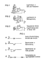
- FIG. 1 shows a first exemplary embodiment of the present invention with a sensor element 1, a converter 2 assigned to it and an operational amplifier 3.
- the sensor element 1 is connected with one of its connections to a supply voltage terminal U0. Its other connection is connected both to the positive input of the operational amplifier 3 and to a first connection of the converter 2, the second connection of which is at ground potential.
- Incident light L causes the sensor element 1 to emit a photocurrent i ph which flows through the converter 2 to earth. Due to the UI characteristic of converter 2, over arises the converter 2 a signal voltage u s , which is at least approximately proportional to the logarithm of the photocurrent i ph , which in turn is proportional to the amount of light incident.
- the operational amplifier is an example of an impedance converter that provides the signal voltage at the output with a level that is practically unchanged compared to the input signal, but with a significantly lower output resistance.
- the sensor element is preferably made of amorphous silicon a-Si: H.
- the converter 2 one can be used whose logarithmic U-I characteristic is determined by a p-n transition in a single-crystalline semiconductor material.
- the converter 2 can also use the logarithmic U-I characteristic of a p-n junction in a polycrystalline semiconductor material.
- the converter 2 uses the non-linear U-I characteristic curve of a layer sequence of one or more layers of amorphous material and the relevant electrode or electrodes.
- the conversion of the photocurrent i ph into the nonlinear voltage signal takes place before signal amplification.
- a voltage drop proportional to the photocurrent i ph is generated across the converter 2 and its output impedance is converted by the operational amplifier 3.
- FIG. 2 shows a further exemplary embodiment with a sensor element 2, an operational amplifier 3 and a converter 2 inserted into a feedback branch of the operational amplifier 3.
- the operational amplifier 3 stands here as an example of an amplifier circuit, in the feedback branch of which the non-linear converter 2 is located.
- the magnitude of the output signal corresponds to that of the circuit according to FIG. 1, however the polarity of the signal is reversed.
- FIG. 3 shows, as already explained, a further exemplary embodiment for the present invention with a sensor element which has the function of the converter and an operational amplifier 3.
- the circuit according to FIG. 3 operates in photovoltaic mode, the logarithmic conversion of the photocurrent into an electrical voltage in the sensor element itself.
- a further development of the invention provides for all of the three circuit arrangements described that at least two elements with a non-linear U-I characteristic are connected in series to increase the signal swing.
- the layer sequence of amorphous silicon a-Si: H consists between two electrodes and that the amorphous silicon is n+-doped in the vicinity of one of the electrodes. It can be expediently provided that that of the two electrodes which lies on the n der-doped layer consists of titanium. The other of the two electrodes then suitably consists of palladium.
- the sensor element 1 and the associated converter 2 form a physical unit, the photovoltaic voltage being the signal voltage u s , which is proportional to the logarithm of the incident light quantity L (see FIG. 3).
- the layer sequence already described can contain the photo element and the converter element in a sandwich-like manner.
- FIG. 4 a, b, c, d each show different implementable embodiments for the converter 2 functioning as a logarithmizer.
- FIG. 4 a shows a diode through which the photocurrent i ph flows and which may have a crystalline or amorphous structure.
- Fig. 4 b shows a further embodiment in which a bipolar transistor is operated in the basic circuit, so that the photocurrent i ph is logarithmic due to the given characteristic of this bipolar transistor.
- 4 c shows a further exemplary embodiment for the converter element, a bipolar transistor being used which is connected as a diode.
- FIG. 4 d finally shows an exemplary embodiment with a series connection of logarithmic elements, which may for example consist of several diodes according to FIG. 4 a.
Landscapes
- Engineering & Computer Science (AREA)
- Multimedia (AREA)
- Signal Processing (AREA)
- Physics & Mathematics (AREA)
- Nonlinear Science (AREA)
- Solid State Image Pick-Up Elements (AREA)
- Light Receiving Elements (AREA)
- Transforming Light Signals Into Electric Signals (AREA)
- Facsimile Heads (AREA)
- Facsimile Scanning Arrangements (AREA)
- Photometry And Measurement Of Optical Pulse Characteristics (AREA)
Abstract
Eine optische Sensorzeile aus amorphem oder polykristallinem photoelektrischem Material mit einer Vielzahl von Sensorelementen, bei der vorgesehen ist, daß jedem Sensorelement (1) ein nichtlineares Element als Konverter (2) zugeordnet ist, der den der einfallenden Lichtmenge proportionalen Photostrom (iph) in eine Signalspannung (us) umwandelt, die zumindest näherungsweise dem Logarithmus des Photostroms (iph) proportional ist. 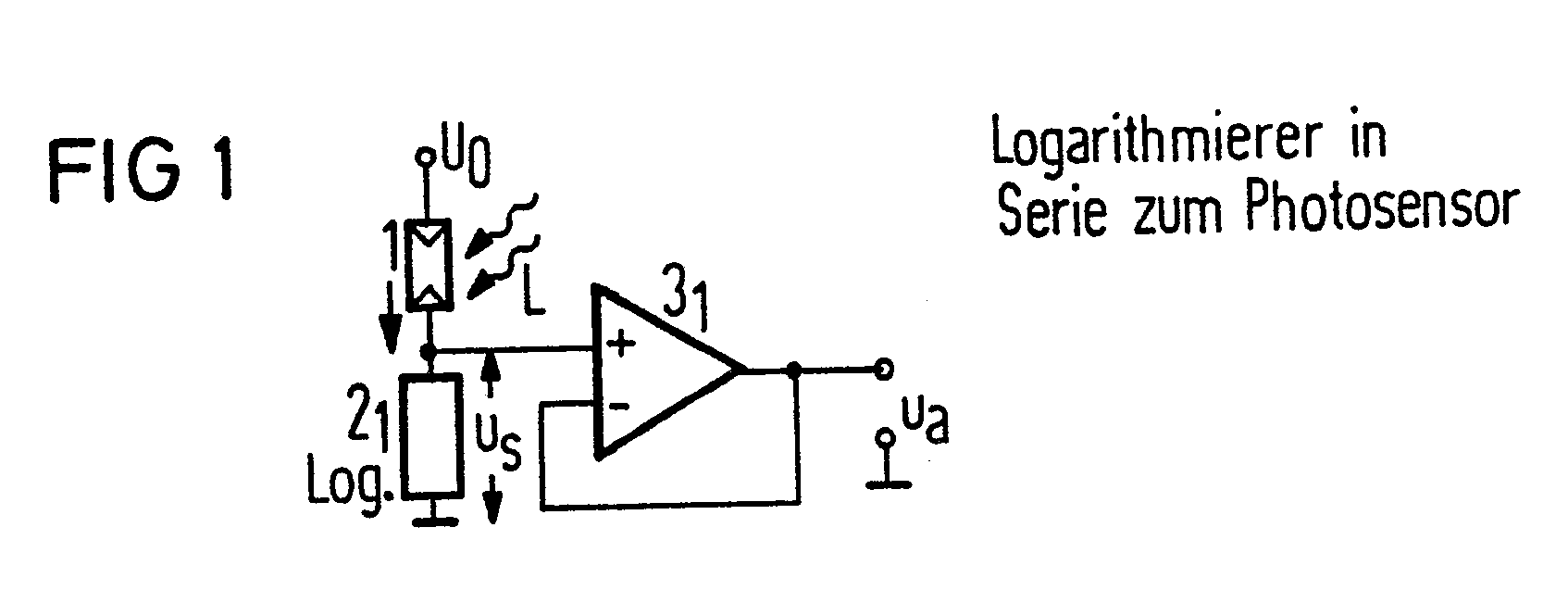
Description
Die vorliegende Erfindung betrifft eine optische Sensorzeile aus amorphem oder polykristallinem photoelektrischem Material mit einer Vielzahl von Sensorelementen.The present invention relates to an optical sensor line made of amorphous or polycrystalline photoelectric material with a plurality of sensor elements.
Die Photoströme von optischen Sensoren steigen näherungsweise linear mit zunehmender Beleuchtungsstärke an, während das menschliche Auge Helligkeiten logarithmisch in Graustufen einteilt. Daraus folgt, daß im dunklen Bereich wesentlich mehr Graustufen in einem vorgegebenen Photostromintervall liegen als im hellen Bereich.The photocurrents from optical sensors increase approximately linearly with increasing illuminance, while the human eye logarithmically divides brightness into grayscale. It follows that there are significantly more gray levels in a given photocurrent interval in the dark area than in the light area.
Beim Auslesen von optischen Abtastzeilen mit amorphen Halbleitersensoren besteht bei hoher Dynamik folgendes Störproblem:When reading out optical scanning lines with amorphous semiconductor sensors, the following interference problem occurs with high dynamics:
Kleine Signale, die beispielsweise um den Faktor 1000 kleiner sind als das Maximum der zu verarbeitenden Signale, gehen in Schalt- und Störsignalen unter. Deshalb ergibt eine lineare Verarbeitung der Photoströme im dunklen Bereich eine geringe Graustufenauflösung.Small signals that are, for example, 1000 times smaller than the maximum of the signals to be processed are lost in switching and interference signals. Therefore, linear processing of the photocurrents in the dark area results in a low grayscale resolution.
Diese Probleme wurden bisher durch eine optimale Leitungsführung, durch eine Vorverstärkung mit hohen Pegeln und niedrigen Ausgangswiderständen und/oder durch eine Störaustastung teilweise verringert.Until now, these problems have been partially reduced by optimal line routing, by preamplification with high levels and low output resistances and / or by noise blanking.
Um eine digitale Datenübertragung der Graustufen mit hoher Auflösung im dunklen Bereich zu gewährleisten, ergibt sich im hellen Bereich eine überflüssig große Anzahl von Graustufen, wenn die Graustufen-Einteilung wie bisher üblich linear erfolgt.In order to ensure digital data transmission of the gray levels with high resolution in the dark area, there is an unnecessarily large number of gray levels in the bright area if the gray level classification is linear as usual.
Der vorliegenden Erfindung liegt die Aufgabe zugrunde, eine optische Sensorzeile der eingangs genannten Art und gemäß dem Oberbegriff des Patentanspruchs 1 zu schaffen, die den Nachteil einer geringen Graustufenauflösung im dunklen Bereich vermeidet und außerdem die für eine digitale Datenübertragung und/oder -verarbeitung der Grauwerte benötigte Bitzahl minimiert.The present invention has for its object to provide an optical sensor line of the type mentioned and according to the preamble of claim 1, which avoids the disadvantage of a low gray level resolution in the dark area and also required for digital data transmission and / or processing of the gray values Number of bits minimized.
Die genannte Aufgabe für die vorliegende Erfindung wird durch eine optische Sensorzeile gemäß dem Oberbegriff des Patentanspruchs 1 gelöst, die erfindungsgemäß dadurch gekennzeichnet ist, daß jedem Sensorelement ein nichtlineares Element als Konverter zugeordnet ist, der den der einfallenden Lichtmenge proportionalen Photostrom in eine Signalspannung umwandelt, die zumindest näherungsweise dem Logarithmus des Photostroms proportional ist.The stated object for the present invention is achieved by an optical sensor line according to the preamble of patent claim 1, which is characterized according to the invention in that each sensor element is assigned a non-linear element as a converter, which converts the photocurrent proportional to the incident quantity of light into a signal voltage which is at least approximately proportional to the logarithm of the photocurrent.
Vorteilhafte weiterbildungen der Erfindung sind durch die in den Unteransprüchen angegebenen Merkmale gekennzeichnet.Advantageous developments of the invention are characterized by the features specified in the subclaims.
Im folgenden wird die Erfindung anhand mehrerer, bevorzugte Ausführungsbeispiele für die vorliegende Erfindung betreffender Figuren im einzelnen erläutert.The invention is explained in detail below with reference to several preferred exemplary embodiments of the figures relating to the present invention.
Die Figuren 1 bis 7 zeigen jeweils die Schaltung für ein Sensorelement stellvertretend für eine komplette Sensorzeile.
- Fig. 1 zeigt ein erstes Ausführungsbeispiel für die vorliegende Erfindung mit einem Sensorelement, einem diesem zugeordneten Konverter und einem Operationsverstärker.
- Fig. 2 zeigt ein weiteres Ausführungsbeispiel mit einem Sensorelement, einem Operationsverstärker und einem in einen Rückkopplungszweig des Operationsverstärkers eingefügten Konverter.
- Fig. 3 zeigt ein weiteres Ausführungsbeispiel für die vorliegende Erfindung mit einem Sensorelement, das in sich die Funktion des Konverters aufweist, und einem Operationsverstärker.
- Fig. 4 a, b, c, d zeigen jeweils verschiedene Ausführungsarten für gemäß der Erfindung zu verwendende Konverter.
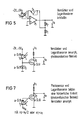
- Fig. 5 zeigt ein erstes Ausführungsbeispiel für eine Schaltungsanordnung, die je Sensorelement vorgesehen ist.
- Fig. 6 zeigt ein zweites Ausführungsbeispiel für eine Schaltungsanordnung, die je Sensorelement vorgesehen ist.
- Fig. 7 zeigt ein drittes Ausführungsbeispiel für eine Schaltungsanordnung, die je Sensorelement vorgesehen ist.
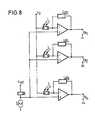
- Fig. 8 zeigt ein bevorzugtes Ausführungsbeispiel für eine Schaltungsanordnung mit Temperaturkompensation für eine Sensorzeile mit n Sensorelementen.
- 1 shows a first exemplary embodiment of the present invention with a sensor element, a converter assigned to it and an operational amplifier.
- FIG. 2 shows a further exemplary embodiment with a sensor element, an operational amplifier and a converter inserted into a feedback branch of the operational amplifier.
- FIG. 3 shows a further exemplary embodiment for the present invention with a sensor element which has the function of the converter and an operational amplifier.
- 4 a, b, c, d each show different embodiments for converters to be used according to the invention.
- 5 shows a first exemplary embodiment of a circuit arrangement which is provided for each sensor element.
- 6 shows a second exemplary embodiment of a circuit arrangement which is provided for each sensor element.
- 7 shows a third exemplary embodiment of a circuit arrangement which is provided for each sensor element.
- 8 shows a preferred exemplary embodiment of a circuit arrangement with temperature compensation for a sensor line with n sensor elements.
Wie bereits erläutert, zeigt Fig. 1 ein erstes Ausführungsbeispiel für die vorliegende Erfindung mit einem Sensorelement 1, einem diesem zugeordneten Konverter 2 und einem Operationsverstärker 3. Das Sensorelement 1 ist mit einem seiner Anschlüsse an eine Versorgungsspannungsklemme U₀ angeschlossen. Sein anderer Anschluß ist sowohl mit dem positiven Eingang des Operationsverstärkers 3 als auch mit einem ersten Anschluß des Konverters 2 verbunden, dessen zweiter Anschluß auf Erdpotential liegt. Einfallendes Licht L bewirkt, daß das Sensorelement 1 einen Photostrom iph ausgibt, der durch den Konverter 2 gegen Erde fließt. Aufgrund der U-I-Kennlinie des Konverters 2 entsteht über dem Konverter 2 eine Signalspannung us, die zumindest näherungsweise dem Logarithmus des Photostroms iph proportional ist, der seinerseits der einfallenden Lichtmenge proportional ist.As already explained, FIG. 1 shows a first exemplary embodiment of the present invention with a sensor element 1, a converter 2 assigned to it and an operational amplifier 3. The sensor element 1 is connected with one of its connections to a supply voltage terminal U₀. Its other connection is connected both to the positive input of the operational amplifier 3 and to a first connection of the converter 2, the second connection of which is at ground potential. Incident light L causes the sensor element 1 to emit a photocurrent i ph which flows through the converter 2 to earth. Due to the UI characteristic of converter 2, over arises the converter 2 a signal voltage u s , which is at least approximately proportional to the logarithm of the photocurrent i ph , which in turn is proportional to the amount of light incident.
Der Operationsverstärker steht als Beispiel für einen Impedanzwandler, der die Signalspannung am Ausgang mit praktisch gegenüber dem Eingangssignal unverändertem Pegel, jedoch wesentlich niedrigerem Ausgangswiderstand zur Verfügung stellt.The operational amplifier is an example of an impedance converter that provides the signal voltage at the output with a level that is practically unchanged compared to the input signal, but with a significantly lower output resistance.
Das Sensorelement ist vorzugsweise aus amorphem Silizium a-Si:H hergestellt. Als Konverter 2 kann ein solcher verwendet werden, dessen logarithmische U-I-Kennlinie durch einen p-n-Übergang in einem einkristallinen Halbleitermaterial bestimmt ist. Der Konverter 2 kann jedoch auch die logarithmische U-I-Kennlinie eines p-n-Übergangs in einem polykristallinen Halbleitermaterial ausnutzen. Schließlich kann gemäß einer Weiterbildung der Erfindung auch vorgesehen sein, daß der Konverter 2 die nichtlineare U-I-Kennlinie einer Schichtfolge von einer oder mehreren Schichten aus amorphem Material und der betreffenden Elektrode oder den betreffenden Elektroden ausnutzt.The sensor element is preferably made of amorphous silicon a-Si: H. As the converter 2, one can be used whose logarithmic U-I characteristic is determined by a p-n transition in a single-crystalline semiconductor material. However, the converter 2 can also use the logarithmic U-I characteristic of a p-n junction in a polycrystalline semiconductor material. Finally, according to a development of the invention, it can also be provided that the converter 2 uses the non-linear U-I characteristic curve of a layer sequence of one or more layers of amorphous material and the relevant electrode or electrodes.
In der beschriebenen Schaltungsanordnung gemäß dem ersten Ausführungsbeispiel erfolgt die Konversion des Photostroms iph in das nichtlineare Spannungssignal vor einer Signalverstärkung. Dabei wird ein dem Photostrom iph proportionaler Spannungsabfall über dem Konverter 2 erzeugt und durch den Operationsverstärker 3 in seiner Ausgangsimpedanz gewandelt.In the circuit arrangement described according to the first exemplary embodiment, the conversion of the photocurrent i ph into the nonlinear voltage signal takes place before signal amplification. A voltage drop proportional to the photocurrent i ph is generated across the converter 2 and its output impedance is converted by the operational amplifier 3.
Fig. 2 zeigt, wie bereits erläutert, ein weiteres Ausführungsbeispiel mit einem Sensorelement 2, einem Operationsverstärker 3 und einem in einen Rückkopplungszweig des Operationsverstärkers 3 eingefügten Konverter 2.As already explained, FIG. 2 shows a further exemplary embodiment with a sensor element 2, an operational amplifier 3 and a converter 2 inserted into a feedback branch of the operational amplifier 3.
Der Operationsverstärker 3 steht hier als Beispiel für eine Verstärkerschaltung, in deren Rückkopplungszweig sich der nichtlineare Konverter 2 befindet. Der Betrag des Ausgangssignals entspricht dem von der Schaltung gemäß Fig. 1, jedoch ist die Polarität des Signals umgekehrt.The operational amplifier 3 stands here as an example of an amplifier circuit, in the feedback branch of which the non-linear converter 2 is located. The magnitude of the output signal corresponds to that of the circuit according to FIG. 1, however the polarity of the signal is reversed.
Fig. 3 zeigt, wie bereits erläutert, ein weiteres Ausführungsbeispiel für die vorliegende Erfindung mit einem Sensorelement, das in sich die Funktion des Konverters aufweist und einem Operationsverstärker 3. Die Schaltung gemäß Fig. 3 arbeitet im photovoltaischen Betrieb, wobei die logarithmische Konversion des Photostroms in eine elektrische Spannung im Sensorelement selbst erfolgt.FIG. 3 shows, as already explained, a further exemplary embodiment for the present invention with a sensor element which has the function of the converter and an operational amplifier 3. The circuit according to FIG. 3 operates in photovoltaic mode, the logarithmic conversion of the photocurrent into an electrical voltage in the sensor element itself.
Eine Weiterbildung der Erfindung sieht für alle der drei beschriebenen Schaltungsanordnungen vor, daß zur Vergrößerung des Signalhubes zumindest zwei Elemente mit nichtlinearer U-I-Kennlinie in Reihe geschaltet sind.A further development of the invention provides for all of the three circuit arrangements described that at least two elements with a non-linear U-I characteristic are connected in series to increase the signal swing.
Gemäß einer anderen Weiterbildung der Erfindung ist vorgesehen, daß die Schichtfolge aus amorphem Silizium a-Si:H zwischen zwei Elektroden besteht und daß das amorphe Silizium in der Nähe einer der Elektroden n⁺-dotiert ist. Hierbei kann zweckmäßig vorgesehen sein, daß diejenige der zwei Elektroden, die an der n⁺-dotierten Schicht liegt, aus Titan besteht. Die andere der zwei Elektroden besteht dann zweckmäßig aus Palladium.According to another development of the invention, it is provided that the layer sequence of amorphous silicon a-Si: H consists between two electrodes and that the amorphous silicon is n⁺-doped in the vicinity of one of the electrodes. It can be expediently provided that that of the two electrodes which lies on the n der-doped layer consists of titanium. The other of the two electrodes then suitably consists of palladium.
Gemäß einer anderen Weiterbildung der Erfindung ist vorgesehen, daß das Sensorelement 1 und der zugeordnete Konverter 2 eine körperliche Einheit bilden, wobei die photovoltaische Spannung die Signalspannung us ist, die dem Logarithmus der einfallenden Lichtmenge L proportional ist (vergl. Fig. 3).According to another development of the invention, it is provided that the sensor element 1 and the associated converter 2 form a physical unit, the photovoltaic voltage being the signal voltage u s , which is proportional to the logarithm of the incident light quantity L (see FIG. 3).
Die zuvor bereits beschriebene Schichtfolge kann gemäß einer weiteren Ausgestaltung der Erfindung sandwichartig das Photoelement und das Konverterelement enthalten.According to a further embodiment of the invention, the layer sequence already described can contain the photo element and the converter element in a sandwich-like manner.
Fig. 4 a, b, c, d zeigen jeweils verschiedene realisierbare Ausführungsformen für den als Logarithmierer fungierenden Konverter 2. Fig. 4 a zeigt eine Diode die in Durchlaßrichtung von dem Photostrom iph durchflossen ist und die einen kristallinen oder amorphen Aufbau aufweisen kann. Fig. 4 b zeigt ein weiteres Ausführungsbeispiel, bei dem ein Bipolartransistor in Basisschaltung betrieben wird, so daß der Photostrom iph aufgrund der gegebenen Kennlinie dieses Bipolartransistors logarithmiert wird.4 a, b, c, d each show different implementable embodiments for the converter 2 functioning as a logarithmizer. FIG. 4 a shows a diode through which the photocurrent i ph flows and which may have a crystalline or amorphous structure. Fig. 4 b shows a further embodiment in which a bipolar transistor is operated in the basic circuit, so that the photocurrent i ph is logarithmic due to the given characteristic of this bipolar transistor.
Fig. 4 c zeigt ein weiteres Ausführungsbeispiel für das Konverterelement, wobei ein Bipolartransistor verwendet ist, der als Diode geschaltet ist.4 c shows a further exemplary embodiment for the converter element, a bipolar transistor being used which is connected as a diode.
Fig. 4 d zeigt schließlich ein Ausführungsbeispiel mit einer Serienschaltung von logarithmierenden Elementen, die beispielsweise aus mehreren Dioden gemäß Fig. 4 a bestehen können.FIG. 4 d finally shows an exemplary embodiment with a series connection of logarithmic elements, which may for example consist of several diodes according to FIG. 4 a.
Die Figuren 5 - 7 zeigen bevorzugte Ausführungsbeispiele der erfindungsgemäßen Schaltung für je ein Sensorelement. Im einzelnen zeigen:
- Fig. 5 eine Verstärkerschaltung, bei der es mit Hilfe eines einzigen Verstärkers 3 gelingt, daß das Signal am Ausgang sowohl niederohmig zur Verfügung steht als auch in seinem Pegel gegenüber dem Spannungsabfall am
nichtlinearen Konverter 2₅ angehoben wird; - Fig. 6, daß sowohl der in Form einer Diode realisierte nichtlineare Konverter 2₆ als auch der als FET
ausgeführte Verstärker 3₆ aus amorphem Silizium a-Si:H, d.h. aus demselben Material aufgebaut ist; dies hat den Vorteil, daß Sensoren, Konverter und Verstärker in einer einheitlichen Technologie integriert hergestellt werden können; - Fig. 7 zeigt eine Schaltung, bei der der Sensor 1₇ photovoltaisch betrieben wird, d.h. Photosensor und Logarithmierer bilden eine körperliche Einheit. Der
vorgesehene Verstärker 3₇ ist wiederum in einheitlicher Technologie zusammen mit dem Sensor 1₇ hergestellt; - Fig. 8 zeigt eine schematische Darstellung eines bevorzugten Ausführungsbeispiels einer Sensorzeile mit erfindungsgemäßer Ausbildung der Auswerteschaltungen für die Sensorelemente, wobei die Temperaturabhängigkeit der nichtlinearen Kennlinien der Konverter in den einzelnen Auswerteschaltungen durch ein gemeinsames Kompensationsglied mit einem gleichartigen Konverter K wie in den Auswerteschaltungen für n Elemente kompensiert wird. Darüber hinaus kann durch Einstellen eines Potentials uref für die n Elemente ein gemeinsamer Nullpunkt der Ausgangssignale festgelegt werden.
- Fig. 5 shows an amplifier circuit in which it is possible with the help of a single amplifier 3 that the signal at the output is both available with a low resistance and its level is raised compared to the voltage drop across the
nonlinear converter 2₅; - 6 shows that both the nonlinear converter 2₆ implemented in the form of a diode and the
amplifier 3₆ designed as an FET are made of amorphous silicon a-Si: H, ie of the same material; this has the advantage that sensors, converters and amplifiers can be manufactured integrated in a uniform technology; - Fig. 7 shows a circuit in which the sensor 1₇ is operated photovoltaically, ie photosensor and logarithmic form a physical unit. The proposed
amplifier 3₇ is in turn made in a uniform technology together with the sensor 1₇; - 8 shows a schematic representation of a preferred exemplary embodiment of a sensor line with the inventive design of the evaluation circuits for the sensor elements, the temperature dependence of the non-linear characteristics of the converters in the individual evaluation circuits being compensated for by a common compensation element with a converter K of the same type as in the evaluation circuits for n elements becomes. In addition, a common zero point of the output signals can be determined by setting a potential u ref for the n elements.
Claims (17)
Applications Claiming Priority (2)
| Application Number | Priority Date | Filing Date | Title |
|---|---|---|---|
| DE3833159 | 1988-09-29 | ||
| DE3833159 | 1988-09-29 |
Publications (2)
| Publication Number | Publication Date |
|---|---|
| EP0361000A2 true EP0361000A2 (en) | 1990-04-04 |
| EP0361000A3 EP0361000A3 (en) | 1991-10-09 |
Family
ID=6364028
Family Applications (1)
| Application Number | Title | Priority Date | Filing Date |
|---|---|---|---|
| EP19890113256 Withdrawn EP0361000A3 (en) | 1988-09-29 | 1989-07-19 | Optical line sensor with a plurality of sensitive elements, made of a photoelectric material with a polycrystalline or amorphous structure |
Country Status (3)
| Country | Link |
|---|---|
| US (1) | US5025146A (en) |
| EP (1) | EP0361000A3 (en) |
| JP (1) | JPH02262779A (en) |
Cited By (1)
| Publication number | Priority date | Publication date | Assignee | Title |
|---|---|---|---|---|
| EP0692907A1 (en) * | 1994-07-12 | 1996-01-17 | Thomson-Csf Semiconducteurs Specifiques | Circuit for suppressing the dark current of a photodetector |
Families Citing this family (3)
| Publication number | Priority date | Publication date | Assignee | Title |
|---|---|---|---|---|
| DE19946983C1 (en) | 1999-09-30 | 2001-04-19 | Infineon Technologies Ag | Arrangement with image sensors |
| ITUD20020139A1 (en) * | 2002-06-19 | 2003-12-19 | Neuricam Spa | PHOTOSENSITIVE ELEMENT FOR ELECTRO-OPTICAL SENSORS |
| DE10254325A1 (en) * | 2002-11-21 | 2004-06-03 | Philips Intellectual Property & Standards Gmbh | Electronic memory component |
Family Cites Families (7)
| Publication number | Priority date | Publication date | Assignee | Title |
|---|---|---|---|---|
| US4309604A (en) * | 1978-07-24 | 1982-01-05 | Sharp Kabushiki Kaisha | Apparatus for sensing the wavelength and intensity of light |
| DE3427055A1 (en) * | 1984-07-23 | 1986-01-30 | Ernst Leitz Wetzlar Gmbh, 6330 Wetzlar | CIRCUIT ARRANGEMENT FOR AN ELECTRONIC EXPOSURE GAUGE |
| US4660075A (en) * | 1983-10-28 | 1987-04-21 | Canon Kabushiki Kaisha | Color information detecting device |
| DE3408284C1 (en) * | 1984-03-07 | 1985-08-29 | Telefunken electronic GmbH, 7100 Heilbronn | Unipolar current amplifier for photodiodes |
| DE8524244U1 (en) * | 1985-08-23 | 1987-02-19 | Siemens AG, 1000 Berlin und 8000 München | High blocking diode array based on a-Si:H for image sensor lines |
| DE3706252A1 (en) * | 1986-02-28 | 1987-09-03 | Canon Kk | Semiconductor photoelectric sensor |
| DE3633182C2 (en) * | 1986-09-30 | 1997-09-11 | Heimann Optoelectronics Gmbh | Optical sensor arrangement |
-
1989
- 1989-07-19 EP EP19890113256 patent/EP0361000A3/en not_active Withdrawn
- 1989-07-31 US US07/386,604 patent/US5025146A/en not_active Expired - Fee Related
- 1989-09-27 JP JP1253718A patent/JPH02262779A/en active Pending
Cited By (3)
| Publication number | Priority date | Publication date | Assignee | Title |
|---|---|---|---|---|
| EP0692907A1 (en) * | 1994-07-12 | 1996-01-17 | Thomson-Csf Semiconducteurs Specifiques | Circuit for suppressing the dark current of a photodetector |
| FR2722635A1 (en) * | 1994-07-12 | 1996-01-19 | Thomson Csf Semiconducteurs | PHOTODETECTOR DARK CURRENT SUPPRESSION CIRCUIT |
| US5656806A (en) * | 1994-07-12 | 1997-08-12 | Thomson-Csf Semiconducteurs Specifiques | Circuit to eliminate the dark current of a photodetector |
Also Published As
| Publication number | Publication date |
|---|---|
| JPH02262779A (en) | 1990-10-25 |
| US5025146A (en) | 1991-06-18 |
| EP0361000A3 (en) | 1991-10-09 |
Similar Documents
| Publication | Publication Date | Title |
|---|---|---|
| DE69419098T2 (en) | METHOD AND DEVICE FOR EQUIPING A LIGHT DETECTOR WITH AN OFFSET | |
| DE69122278T2 (en) | Photoelectric conversion device | |
| DE112018002674T5 (en) | Solid state imaging device and imaging device | |
| DE19737330A1 (en) | Matrix image forming system | |
| DE69427051T2 (en) | Photoelectric conversion device | |
| DE3522314C2 (en) | ||
| DE3006267C2 (en) | Solid-state imaging arrangement | |
| DE3345239A1 (en) | FIXED BODY IMAGE SENSOR | |
| DE2029627B2 (en) | Compensation circuit for an optical scanning device | |
| DE112006001471T5 (en) | Optical sensor circuit and image sensor | |
| DE3135740A1 (en) | PHOTOELECTRIC CONVERSION DEVICE | |
| DE69634712T2 (en) | Switching transistor for a solid-state image pickup device | |
| EP0361000A2 (en) | Optical line sensor with a plurality of sensitive elements, made of a photoelectric material with a polycrystalline or amorphous structure | |
| DE3407665A1 (en) | PHOTOELECTRIC CONVERTER | |
| DE1966819B2 (en) | DEVICE FOR DETERMINING A LIGHT FLOW | |
| DE69632532T2 (en) | MULTIPLEXIC SWITCHING | |
| DE2159036C3 (en) | Exposure control arrangement with a photodiode | |
| DE3543666A1 (en) | METHOD AND CIRCUIT ARRANGEMENT FOR COMPENSATING CHANGES IN THE PARAMETERS OF AN OPTICAL TRANSMITTER AND AN OPTICAL RECEIVER IN AN OPTICAL SCANNER | |
| DE69416474T2 (en) | amplifier | |
| DE2538275B2 (en) | Photoelectric barrier | |
| DE112021007156T5 (en) | PINIONED PHOTODIODE SENSOR | |
| DE3615925A1 (en) | Capacitively coupled integrating-type transimpedance amplifier | |
| DE2610276C2 (en) | Transistor amplifier for alternating current signals | |
| DE19753835A1 (en) | Photocell as proximity sensor with reception members | |
| WO2002032114A1 (en) | Optical sensor |
Legal Events
| Date | Code | Title | Description |
|---|---|---|---|
| PUAI | Public reference made under article 153(3) epc to a published international application that has entered the european phase |
Free format text: ORIGINAL CODE: 0009012 |
|
| AK | Designated contracting states |
Kind code of ref document: A2 Designated state(s): DE FR GB NL |
|
| 17P | Request for examination filed |
Effective date: 19901205 |
|
| PUAL | Search report despatched |
Free format text: ORIGINAL CODE: 0009013 |
|
| AK | Designated contracting states |
Kind code of ref document: A3 Designated state(s): DE FR GB NL |
|
| 17Q | First examination report despatched |
Effective date: 19930908 |
|
| STAA | Information on the status of an ep patent application or granted ep patent |
Free format text: STATUS: THE APPLICATION IS DEEMED TO BE WITHDRAWN |
|
| 18D | Application deemed to be withdrawn |
Effective date: 19940118 |