EP0361000A2 - Capteur de ligne optique muni d'une pluralité d'éléments capteurs réalisés dans un matériau photo-électrique de structure amorphe ou polycristalline - Google Patents
Capteur de ligne optique muni d'une pluralité d'éléments capteurs réalisés dans un matériau photo-électrique de structure amorphe ou polycristalline Download PDFInfo
- Publication number
- EP0361000A2 EP0361000A2 EP89113256A EP89113256A EP0361000A2 EP 0361000 A2 EP0361000 A2 EP 0361000A2 EP 89113256 A EP89113256 A EP 89113256A EP 89113256 A EP89113256 A EP 89113256A EP 0361000 A2 EP0361000 A2 EP 0361000A2
- Authority
- EP
- European Patent Office
- Prior art keywords
- optical sensor
- line according
- sensor line
- converter
- linear
- Prior art date
- Legal status (The legal status is an assumption and is not a legal conclusion. Google has not performed a legal analysis and makes no representation as to the accuracy of the status listed.)
- Withdrawn
Links
Images
Classifications
-
- H—ELECTRICITY
- H04—ELECTRIC COMMUNICATION TECHNIQUE
- H04N—PICTORIAL COMMUNICATION, e.g. TELEVISION
- H04N25/00—Circuitry of solid-state image sensors [SSIS]; Control thereof
- H04N25/50—Control of the SSIS exposure
- H04N25/57—Control of the dynamic range
- H04N25/571—Control of the dynamic range involving a non-linear response
- H04N25/573—Control of the dynamic range involving a non-linear response the logarithmic type
-
- H—ELECTRICITY
- H04—ELECTRIC COMMUNICATION TECHNIQUE
- H04N—PICTORIAL COMMUNICATION, e.g. TELEVISION
- H04N25/00—Circuitry of solid-state image sensors [SSIS]; Control thereof
-
- H—ELECTRICITY
- H04—ELECTRIC COMMUNICATION TECHNIQUE
- H04N—PICTORIAL COMMUNICATION, e.g. TELEVISION
- H04N25/00—Circuitry of solid-state image sensors [SSIS]; Control thereof
- H04N25/70—SSIS architectures; Circuits associated therewith
- H04N25/701—Line sensors
Definitions
- the present invention relates to an optical sensor line made of amorphous or polycrystalline photoelectric material with a plurality of sensor elements.
- the photocurrents from optical sensors increase approximately linearly with increasing illuminance, while the human eye logarithmically divides brightness into grayscale. It follows that there are significantly more gray levels in a given photocurrent interval in the dark area than in the light area.
- the present invention has for its object to provide an optical sensor line of the type mentioned and according to the preamble of claim 1, which avoids the disadvantage of a low gray level resolution in the dark area and also required for digital data transmission and / or processing of the gray values Number of bits minimized.
- each sensor element is assigned a non-linear element as a converter, which converts the photocurrent proportional to the incident quantity of light into a signal voltage which is at least approximately proportional to the logarithm of the photocurrent.
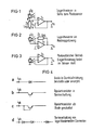
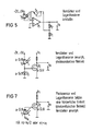
- FIG. 1 shows a first exemplary embodiment of the present invention with a sensor element 1, a converter 2 assigned to it and an operational amplifier 3.
- the sensor element 1 is connected with one of its connections to a supply voltage terminal U0. Its other connection is connected both to the positive input of the operational amplifier 3 and to a first connection of the converter 2, the second connection of which is at ground potential.
- Incident light L causes the sensor element 1 to emit a photocurrent i ph which flows through the converter 2 to earth. Due to the UI characteristic of converter 2, over arises the converter 2 a signal voltage u s , which is at least approximately proportional to the logarithm of the photocurrent i ph , which in turn is proportional to the amount of light incident.
- the operational amplifier is an example of an impedance converter that provides the signal voltage at the output with a level that is practically unchanged compared to the input signal, but with a significantly lower output resistance.
- the sensor element is preferably made of amorphous silicon a-Si: H.
- the converter 2 one can be used whose logarithmic U-I characteristic is determined by a p-n transition in a single-crystalline semiconductor material.
- the converter 2 can also use the logarithmic U-I characteristic of a p-n junction in a polycrystalline semiconductor material.
- the converter 2 uses the non-linear U-I characteristic curve of a layer sequence of one or more layers of amorphous material and the relevant electrode or electrodes.
- the conversion of the photocurrent i ph into the nonlinear voltage signal takes place before signal amplification.
- a voltage drop proportional to the photocurrent i ph is generated across the converter 2 and its output impedance is converted by the operational amplifier 3.
- FIG. 2 shows a further exemplary embodiment with a sensor element 2, an operational amplifier 3 and a converter 2 inserted into a feedback branch of the operational amplifier 3.
- the operational amplifier 3 stands here as an example of an amplifier circuit, in the feedback branch of which the non-linear converter 2 is located.
- the magnitude of the output signal corresponds to that of the circuit according to FIG. 1, however the polarity of the signal is reversed.
- FIG. 3 shows, as already explained, a further exemplary embodiment for the present invention with a sensor element which has the function of the converter and an operational amplifier 3.
- the circuit according to FIG. 3 operates in photovoltaic mode, the logarithmic conversion of the photocurrent into an electrical voltage in the sensor element itself.
- a further development of the invention provides for all of the three circuit arrangements described that at least two elements with a non-linear U-I characteristic are connected in series to increase the signal swing.
- the layer sequence of amorphous silicon a-Si: H consists between two electrodes and that the amorphous silicon is n+-doped in the vicinity of one of the electrodes. It can be expediently provided that that of the two electrodes which lies on the n der-doped layer consists of titanium. The other of the two electrodes then suitably consists of palladium.
- the sensor element 1 and the associated converter 2 form a physical unit, the photovoltaic voltage being the signal voltage u s , which is proportional to the logarithm of the incident light quantity L (see FIG. 3).
- the layer sequence already described can contain the photo element and the converter element in a sandwich-like manner.
- FIG. 4 a, b, c, d each show different implementable embodiments for the converter 2 functioning as a logarithmizer.
- FIG. 4 a shows a diode through which the photocurrent i ph flows and which may have a crystalline or amorphous structure.
- Fig. 4 b shows a further embodiment in which a bipolar transistor is operated in the basic circuit, so that the photocurrent i ph is logarithmic due to the given characteristic of this bipolar transistor.
- 4 c shows a further exemplary embodiment for the converter element, a bipolar transistor being used which is connected as a diode.
- FIG. 4 d finally shows an exemplary embodiment with a series connection of logarithmic elements, which may for example consist of several diodes according to FIG. 4 a.
Landscapes
- Engineering & Computer Science (AREA)
- Multimedia (AREA)
- Signal Processing (AREA)
- Physics & Mathematics (AREA)
- Nonlinear Science (AREA)
- Solid State Image Pick-Up Elements (AREA)
- Light Receiving Elements (AREA)
- Transforming Light Signals Into Electric Signals (AREA)
- Facsimile Heads (AREA)
- Facsimile Scanning Arrangements (AREA)
- Photometry And Measurement Of Optical Pulse Characteristics (AREA)
Applications Claiming Priority (2)
| Application Number | Priority Date | Filing Date | Title |
|---|---|---|---|
| DE3833159 | 1988-09-29 | ||
| DE3833159 | 1988-09-29 |
Publications (2)
| Publication Number | Publication Date |
|---|---|
| EP0361000A2 true EP0361000A2 (fr) | 1990-04-04 |
| EP0361000A3 EP0361000A3 (fr) | 1991-10-09 |
Family
ID=6364028
Family Applications (1)
| Application Number | Title | Priority Date | Filing Date |
|---|---|---|---|
| EP19890113256 Withdrawn EP0361000A3 (fr) | 1988-09-29 | 1989-07-19 | Capteur de ligne optique muni d'une pluralité d'éléments capteurs réalisés dans un matériau photo-électrique de structure amorphe ou polycristalline |
Country Status (3)
| Country | Link |
|---|---|
| US (1) | US5025146A (fr) |
| EP (1) | EP0361000A3 (fr) |
| JP (1) | JPH02262779A (fr) |
Cited By (1)
| Publication number | Priority date | Publication date | Assignee | Title |
|---|---|---|---|---|
| EP0692907A1 (fr) * | 1994-07-12 | 1996-01-17 | Thomson-Csf Semiconducteurs Specifiques | Circuit de suppression de courant d'obscurité de photodétecteur |
Families Citing this family (3)
| Publication number | Priority date | Publication date | Assignee | Title |
|---|---|---|---|---|
| DE19946983C1 (de) | 1999-09-30 | 2001-04-19 | Infineon Technologies Ag | Anordnung mit Bildsensoren |
| ITUD20020139A1 (it) * | 2002-06-19 | 2003-12-19 | Neuricam Spa | Elemento fotosensibile per sensori elettro-ottici |
| DE10254325A1 (de) * | 2002-11-21 | 2004-06-03 | Philips Intellectual Property & Standards Gmbh | Elektronisches Speicherbauteil |
Family Cites Families (7)
| Publication number | Priority date | Publication date | Assignee | Title |
|---|---|---|---|---|
| US4309604A (en) * | 1978-07-24 | 1982-01-05 | Sharp Kabushiki Kaisha | Apparatus for sensing the wavelength and intensity of light |
| DE3427055A1 (de) * | 1984-07-23 | 1986-01-30 | Ernst Leitz Wetzlar Gmbh, 6330 Wetzlar | Schaltungsanordnung fuer einen elektronischen belichtungsmesser |
| US4660075A (en) * | 1983-10-28 | 1987-04-21 | Canon Kabushiki Kaisha | Color information detecting device |
| DE3408284C1 (de) * | 1984-03-07 | 1985-08-29 | Telefunken electronic GmbH, 7100 Heilbronn | Unipolarer Stromverstärker für Fotodioden |
| DE8524244U1 (de) * | 1985-08-23 | 1987-02-19 | Siemens AG, 1000 Berlin und 8000 München | Hochsperrende Diodenanordnung auf der Basis von a-Si:H für Bildsensorzeilen |
| DE3706252A1 (de) * | 1986-02-28 | 1987-09-03 | Canon Kk | Halbleiterfotosensor |
| DE3633182C2 (de) * | 1986-09-30 | 1997-09-11 | Heimann Optoelectronics Gmbh | Optische Sensoranordnung |
-
1989
- 1989-07-19 EP EP19890113256 patent/EP0361000A3/fr not_active Withdrawn
- 1989-07-31 US US07/386,604 patent/US5025146A/en not_active Expired - Fee Related
- 1989-09-27 JP JP1253718A patent/JPH02262779A/ja active Pending
Cited By (3)
| Publication number | Priority date | Publication date | Assignee | Title |
|---|---|---|---|---|
| EP0692907A1 (fr) * | 1994-07-12 | 1996-01-17 | Thomson-Csf Semiconducteurs Specifiques | Circuit de suppression de courant d'obscurité de photodétecteur |
| FR2722635A1 (fr) * | 1994-07-12 | 1996-01-19 | Thomson Csf Semiconducteurs | Circuit de suppression de courant d'obscurite de photodetecteur |
| US5656806A (en) * | 1994-07-12 | 1997-08-12 | Thomson-Csf Semiconducteurs Specifiques | Circuit to eliminate the dark current of a photodetector |
Also Published As
| Publication number | Publication date |
|---|---|
| JPH02262779A (ja) | 1990-10-25 |
| US5025146A (en) | 1991-06-18 |
| EP0361000A3 (fr) | 1991-10-09 |
Similar Documents
| Publication | Publication Date | Title |
|---|---|---|
| DE69419098T2 (de) | Verfahren und vorrichtung zur ausstattung eines lichtdetektors mit einem offset | |
| DE69122278T2 (de) | Photoelektrische Umwandlungsvorrichtung | |
| DE112018002674T5 (de) | Festkörper-Abbildungsvorrichtung und Abbildungsvorrichtung | |
| DE19737330A1 (de) | Abbildungssystem | |
| DE69427051T2 (de) | Photoelektrische Umwandlungsanordnung | |
| DE3522314C2 (fr) | ||
| DE3006267C2 (de) | Festkörper-Abbildungsanordnung | |
| DE3345239A1 (de) | Festkoerper-bildsensor | |
| DE2029627B2 (de) | Kompensationsschaltung für eine optische Abtasteinrichtung | |
| DE112006001471T5 (de) | Optische Sensorschaltung und Bildsensor | |
| DE3135740A1 (de) | Photoelektrische umsetzeinrichtung | |
| DE69634712T2 (de) | Schalttransistor für eine Festkörperbildaufnahmevorrichtung | |
| EP0361000A2 (fr) | Capteur de ligne optique muni d'une pluralité d'éléments capteurs réalisés dans un matériau photo-électrique de structure amorphe ou polycristalline | |
| DE3407665A1 (de) | Fotoelektrischer wandler | |
| DE1966819B2 (de) | Vorrichtung zur bestimmung eines lichtstromes | |
| DE69632532T2 (de) | Multiplexe schaltung | |
| DE2159036C3 (de) | Belichtungssteueranordnung mit einer Fotodiode | |
| DE3543666A1 (de) | Verfahren und schaltungsanordnung zur kompensation von aenderungen der parameter eines optischen senders und eines optischen empfaengers in einem optischen abtaster | |
| DE69416474T2 (de) | Verstärker | |
| DE2538275B2 (de) | Lichtschranke | |
| DE112021007156T5 (de) | Gestifteter fotodioden-sensor | |
| DE3615925A1 (de) | Integrierender kapazitiv gekoppelter transimpedanzverstaerker | |
| DE2610276C2 (de) | Transistorverstärker für Wechselstromsignale | |
| DE19753835A1 (de) | Näherungsfühler mit schnellem Empfangsverstärker | |
| WO2002032114A1 (fr) | Capteur optique |
Legal Events
| Date | Code | Title | Description |
|---|---|---|---|
| PUAI | Public reference made under article 153(3) epc to a published international application that has entered the european phase |
Free format text: ORIGINAL CODE: 0009012 |
|
| AK | Designated contracting states |
Kind code of ref document: A2 Designated state(s): DE FR GB NL |
|
| 17P | Request for examination filed |
Effective date: 19901205 |
|
| PUAL | Search report despatched |
Free format text: ORIGINAL CODE: 0009013 |
|
| AK | Designated contracting states |
Kind code of ref document: A3 Designated state(s): DE FR GB NL |
|
| 17Q | First examination report despatched |
Effective date: 19930908 |
|
| STAA | Information on the status of an ep patent application or granted ep patent |
Free format text: STATUS: THE APPLICATION IS DEEMED TO BE WITHDRAWN |
|
| 18D | Application deemed to be withdrawn |
Effective date: 19940118 |