EP0361194A2 - Procédé pour enrober des composants ou assemblages de composants électriques ou électroniques et enrobage pour des composants ou assemblages de composants électriques ou électroniques - Google Patents
Procédé pour enrober des composants ou assemblages de composants électriques ou électroniques et enrobage pour des composants ou assemblages de composants électriques ou électroniques Download PDFInfo
- Publication number
- EP0361194A2 EP0361194A2 EP89116803A EP89116803A EP0361194A2 EP 0361194 A2 EP0361194 A2 EP 0361194A2 EP 89116803 A EP89116803 A EP 89116803A EP 89116803 A EP89116803 A EP 89116803A EP 0361194 A2 EP0361194 A2 EP 0361194A2
- Authority
- EP
- European Patent Office
- Prior art keywords
- intermediate layer
- injection
- molding compound
- layer
- mold
- Prior art date
- Legal status (The legal status is an assumption and is not a legal conclusion. Google has not performed a legal analysis and makes no representation as to the accuracy of the status listed.)
- Withdrawn
Links
Images

Classifications
-
- B—PERFORMING OPERATIONS; TRANSPORTING
- B29—WORKING OF PLASTICS; WORKING OF SUBSTANCES IN A PLASTIC STATE IN GENERAL
- B29C—SHAPING OR JOINING OF PLASTICS; SHAPING OF MATERIAL IN A PLASTIC STATE, NOT OTHERWISE PROVIDED FOR; AFTER-TREATMENT OF THE SHAPED PRODUCTS, e.g. REPAIRING
- B29C45/00—Injection moulding, i.e. forcing the required volume of moulding material through a nozzle into a closed mould; Apparatus therefor
- B29C45/14—Injection moulding, i.e. forcing the required volume of moulding material through a nozzle into a closed mould; Apparatus therefor incorporating preformed parts or layers, e.g. injection moulding around inserts or for coating articles
- B29C45/14639—Injection moulding, i.e. forcing the required volume of moulding material through a nozzle into a closed mould; Apparatus therefor incorporating preformed parts or layers, e.g. injection moulding around inserts or for coating articles for obtaining an insulating effect, e.g. for electrical components
- B29C45/14655—Injection moulding, i.e. forcing the required volume of moulding material through a nozzle into a closed mould; Apparatus therefor incorporating preformed parts or layers, e.g. injection moulding around inserts or for coating articles for obtaining an insulating effect, e.g. for electrical components connected to or mounted on a carrier, e.g. lead frame
-
- B—PERFORMING OPERATIONS; TRANSPORTING
- B29—WORKING OF PLASTICS; WORKING OF SUBSTANCES IN A PLASTIC STATE IN GENERAL
- B29C—SHAPING OR JOINING OF PLASTICS; SHAPING OF MATERIAL IN A PLASTIC STATE, NOT OTHERWISE PROVIDED FOR; AFTER-TREATMENT OF THE SHAPED PRODUCTS, e.g. REPAIRING
- B29C45/00—Injection moulding, i.e. forcing the required volume of moulding material through a nozzle into a closed mould; Apparatus therefor
- B29C45/16—Making multilayered or multicoloured articles
- B29C45/1635—Making multilayered or multicoloured articles using displaceable mould parts, e.g. retractable partition between adjacent mould cavities
-
- B—PERFORMING OPERATIONS; TRANSPORTING
- B29—WORKING OF PLASTICS; WORKING OF SUBSTANCES IN A PLASTIC STATE IN GENERAL
- B29C—SHAPING OR JOINING OF PLASTICS; SHAPING OF MATERIAL IN A PLASTIC STATE, NOT OTHERWISE PROVIDED FOR; AFTER-TREATMENT OF THE SHAPED PRODUCTS, e.g. REPAIRING
- B29C45/00—Injection moulding, i.e. forcing the required volume of moulding material through a nozzle into a closed mould; Apparatus therefor
- B29C45/16—Making multilayered or multicoloured articles
- B29C45/1671—Making multilayered or multicoloured articles with an insert
-
- H—ELECTRICITY
- H10—SEMICONDUCTOR DEVICES; ELECTRIC SOLID-STATE DEVICES NOT OTHERWISE PROVIDED FOR
- H10W—GENERIC PACKAGES, INTERCONNECTIONS, CONNECTORS OR OTHER CONSTRUCTIONAL DETAILS OF DEVICES COVERED BY CLASS H10
- H10W74/00—Encapsulations, e.g. protective coatings
- H10W74/01—Manufacture or treatment
- H10W74/016—Manufacture or treatment using moulds
-
- H—ELECTRICITY
- H10—SEMICONDUCTOR DEVICES; ELECTRIC SOLID-STATE DEVICES NOT OTHERWISE PROVIDED FOR
- H10W—GENERIC PACKAGES, INTERCONNECTIONS, CONNECTORS OR OTHER CONSTRUCTIONAL DETAILS OF DEVICES COVERED BY CLASS H10
- H10W74/00—Encapsulations, e.g. protective coatings
- H10W74/40—Encapsulations, e.g. protective coatings characterised by their materials
- H10W74/47—Encapsulations, e.g. protective coatings characterised by their materials comprising organic materials, e.g. plastics or resins
-
- H—ELECTRICITY
- H10—SEMICONDUCTOR DEVICES; ELECTRIC SOLID-STATE DEVICES NOT OTHERWISE PROVIDED FOR
- H10W—GENERIC PACKAGES, INTERCONNECTIONS, CONNECTORS OR OTHER CONSTRUCTIONAL DETAILS OF DEVICES COVERED BY CLASS H10
- H10W90/00—Package configurations
- H10W90/701—Package configurations characterised by the relative positions of pads or connectors relative to package parts
- H10W90/751—Package configurations characterised by the relative positions of pads or connectors relative to package parts of bond wires
- H10W90/756—Package configurations characterised by the relative positions of pads or connectors relative to package parts of bond wires between a chip and a stacked lead frame, conducting package substrate or heat sink
Definitions
- the invention relates to a method for wrapping electrical and electronic components or assemblies, in which an intermediate layer made of an elastic plastic and then an outer wrapping layer made of a mechanically and chemically stable plastic are first applied to the mechanically sensitive areas, and a wrapping for electrical and Electronic components or assemblies with an intermediate layer made of an elastic plastic applied to the mechanically sensitive areas and an outer covering layer made of a mechanically and chemically stable plastic.
- thermoset-encased electronic components such as integrated circuits, or assemblies, such as hybrid circuits
- the internal stresses are generated by plastic shrinkage and by different thermal expansions of the component or assembly, system carrier and plastic.
- a coating is therefore required which both compensates for the stresses and the different expansions and also offers protection against internal corrosion.
- integrated circuits for example, are currently covered in a cost-intensive manner before the thermosetting coating with a protective layer, which consists, for example, of plasma nitride, polyimide and / or gel drops.
- a protective layer which consists, for example, of plasma nitride, polyimide and / or gel drops.
- the areas outside the chip such as the chip circumference and the bond wire / lead contact point, remain unprotected.
- an elastic intermediate layer is used to protect the components and the circuit, which consists for example of silicone gel or an elastic acrylate.
- DE-A-34 42 131 discloses a method for enveloping microelectronic hybrid semiconductor circuits or of microelectronic semiconductor components, in which the components located on a substrate are covered with a soft, sealable plastic layer, covered with a plastic-metal composite film and then encapsulated with synthetic resin.
- a soft, sealable plastic layer covered with a plastic-metal composite film and then encapsulated with synthetic resin.
- a low-viscosity, liquid elastomer is applied as a soft, sealable plastic layer.
- a plastic-metal composite film is then placed on this layer and pressed with a heated hollow punch.
- a synthetic resin in particular a highly filled epoxy resin, is then used for the subsequent casting or encapsulation.
- a low-voltage covering for electrical and electronic components, in particular hybrid circuits is proposed, in which an elastic and compressible intermediate layer is first applied to the mechanically sensitive areas and then a mechanically and chemically stable outer covering layer.
- a two-component polyurethane is added, in which the formation of small amounts of bubbles leads to the formation of bubbles.
- a UV-curing silicone rubber is used for the intermediate layer, in which micro-hollow bodies made of polyvinylidene chloride (PVDC) are mixed.
- PVDC polyvinylidene chloride
- the invention has for its object to provide an economical and easily automated method for wrapping electrical or electronic components or assemblies, which enables compensation of voltages and different strains and also offers reliable protection against internal corrosion. Furthermore, one of the above mentioned sufficient wrapping must be specified.
- this object is achieved according to the invention in that the outer coating layer is applied in the hollow mold of an injection molding tool by injection molding a molding compound.
- the invention is based on the knowledge that the particularly economical injection molding can be used due to the advantages of an elastic intermediate layer for the application of the outer covering layer.
- Injection molding is to be seen here as a master form that, when machine and tool conditions are exploited, leads from the molding compound to the finished outer coating layer in a single step performed by the machine.
- the advantages over the conventional casting with synthetic resin lie in the economical and easily automated working method, in which the need for dosing is eliminated, the low waste, and in the practically unlimited storage life of the material used. There is no loss of reaction, i.e. the shrinkage is only caused by thermal expansion.
- thermoplastic molding composition is used for the outer covering layer, which is particularly well suited for processing by injection molding due to its thermoplasticity.
- partially crystalline and in particular also liquid-crystalline thermoplastics have proven particularly useful as molding compositions.
- the intermediate layer is applied in the hollow mold of a first injection mold by injection molding a molding compound.
- injection molding a molding compound.
- thermoplastic elastomers are particularly suitable, since they can be easily processed by injection molding.
- the use of elastically compressible polymers as a molding compound for the intermediate layer has further advantages.
- elastically compressible polymers with a microcellular foam structure can be used as an easily processable molding compound. Problem-free injection molding processing also results, however, if elastically compressible polymers with elastic micro hollow bodies are used as filler for the intermediate layer.
- the hollow mold of the first injection mold is not completely filled during the injection molding of the intermediate layer. With such a remaining volume reserve during injection molding, the mold internal pressure can remain extremely low, so that so-called wire drifts and similar phenomena can be safely avoided.
- the intermediate layer is applied in the form of a one-sided cover, the opposite side being supported by a controllable tool insert of the first injection mold.
- the controllable tool insert acts here as a counterbearing of the system carrier island or the like.
- the same lower part of the tool with controllable tool insert can then also be used for applying the intermediate layer in the first injection mold and for applying the outer covering layer in the second injection mold.
- the controllable tool insert then acts as a counter-bearing when the intermediate layer is applied, while it is retracted when the outer casing is applied, thereby creating the required cavity in the lower part of the tool.
- the invention also provides a covering for electrical and electronic components or assemblies with an intermediate layer applied to the mechanically sensitive areas made of an elastic plastic and an outer covering layer made of a mechanically and chemically stable plastic, in which the outer covering layer consists of an injection molded thermoplastic and can therefore be produced particularly economically.
- the intermediate layer if it consists of an injection-molded thermoplastic elastomer or an injection-molded elastic-compressible polymer.
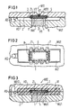
- FIG. 1 shows the two-stage wrapping of an integrated circuit.
- the module which is referred to as an IC as a whole, consists of a chip 1 which is arranged on a system carrier 2 and the connections of which are connected to the associated connecting legs of the system carrier 2 via fine bonding wires 3.
- the outer regions of the system carrier 2 are tightly between the upper tool part WO11 and the lower tool part WU1 of a first injection molding tool W11 are arranged, while the chip 1 and the mechanically sensitive areas on the chip circumference with the contact points of the bonding wires 3 are located within the hollow mold H11 of the first injection molding tool W11.
- a controllable tool insert We1 which can be moved vertically in the direction of the double arrow Pf1 and which, in its upper position shown in FIG. 1, acts as a counterbearing for the system carrier island 4.
- the hollow mold H11 is then filled with a thermoplastic elastomer via a sprue bushing A11, but the filling is not complete and a certain volume reserve 5 remains.
- this volume reserve 5 the mold internal pressure during injection molding can remain extremely low, ie drifts in the bond wires 3 are avoided with certainty.
- the first injection molding process described above produces an elastic intermediate layer Z1 which, according to the plan view shown in FIG. 2 with the upper part WO11 of the tool removed, in addition to a complete covering of the chip 1, simultaneously the chip edges 6 and all the bonding wires 3 completely beyond those on the connecting legs 7 also wedge edges 8 around.
- the wedge edges 8 are contact points that were created during the so-called wedge bonding of the bonding wires 3. It is easy to see that the mechanically sensitive areas, in particular the chip area and the adjacent connection area, are protected by the elastic intermediate layer Z1.
- the controllable tool insert We1 is moved into its lower position according to FIG. 3, and the lower tool part WU1 is combined with a second upper tool part WO12, which results in a second injection mold, which is designated W12 overall.
- a high-strength thermoplastic molding compound is then injected into the hollow mold H12 of this second injection molding tool W12 via an end connection A12, which has an outer surface cladding layer U1 forms.
- this outer wrapping layer U1 is injection molded, a pressure is exerted on the intermediate layer Z1, which produces an elastically adherent, dense cushion.
- the same lower tool part WU1 can thus be used for the injection molding of the intermediate layer Z1 and the injection molding of the outer sheathing layer U1, this double use being made possible by the controllable tool insert We1.
- FIGS. 4 and 5 show the two-stage encasing of an assembly 10, of which components 102 and 103, bond wires 104 and external connections 105 arranged on a substrate 101 can be seen.
- This assembly 10 is now first introduced according to FIG. 4 into a first injection mold W21, in the upper part WO21 of which there is a hollow mold H21 adapted to the surface of the substrate 101.
- a controllable tool insert We2 which can be moved vertically in the direction of the double arrow Pf2 and which, in its upper position shown in FIG. 4, supports the entire substrate 101 from below.
- the hollow mold H21 is then filled via a sprue bushing A21 with a thermoplastic elastomer, which covers the entire substrate area and forms an elastic intermediate layer Z2.
- the controllable tool insert We2 is moved into its lower position shown in FIG. 5 and a second tool upper part WO22 is placed on the lower tool part WU2. This creates a second injection molding tool W22, in the cavity H22 of which a thermoplastic molding compound of high strength is injected under pressure to form an outer covering layer U2.
- this elastic or elastically compressible layer could also, for example, by Pouring or dosing can be applied.
- the sheathing of the assembly 10 described with reference to FIGS. 4 and 5 can also be used for sealing an assembly preassembled in a frame-like housing body or a component preassembled in a lower housing part.
- thermoplastic elastomers are preferably used as the molding compound during injection molding of the intermediate layer Z1 or Z2, for example polyolefin-based elastomers .
- Polyethers, polyurethanes or polyether esters are suitable.
- molding compositions which have proven themselves in practical testing in particular olefin-diene terpolymers (trade name "Nordel” from EI du Pont de Nemours & Co. Inc. Wilmington, Delaware US) and polyether esters (trade name "Hytrel” from EI du Pont de Nemours) & Co. Inc.
- corresponding injection-moldable elastic-compressible polymer materials can also be used, which have, for example, a microcellular structure or elastic micro hollow bodies as fillers.
- a microcellular structure or elastic micro hollow bodies as fillers.
- 10 to 15% by volume of micro-hollow bodies made of polyvinylidene chloride (PVDC) with an average diameter of 40 ⁇ m and a wall thickness of approximately 0.5 ⁇ m (product from Follmann & Co.) can be mixed into the molding composition.
- PVDC polyvinylidene chloride
- Thermoplastic molding compositions are preferably used for the injection molding of the outer cladding layers U1 or U2.
- Polyphenylene sulfide (PPS) (trade name "Ryton” from Phillips Petroleum Co., Bartlesville, US) can be mentioned as an example of partially crystalline thermoplastics.
- Polyphenylene sulfide is characterized by a very high temperature resistance up to 260 oC .
- outer coating layers U1 and U2 based on liquid-crystalline thermoplastics are a molding compound available under the trade name "Vectra” (Celanese Corp. of America, New York, NY, US) and a molding compound available under the trade name "Ultrax” ( BASF AG, Ludwigshafen, DE).
Landscapes
- Engineering & Computer Science (AREA)
- Manufacturing & Machinery (AREA)
- Mechanical Engineering (AREA)
- Injection Moulding Of Plastics Or The Like (AREA)
Applications Claiming Priority (2)
| Application Number | Priority Date | Filing Date | Title |
|---|---|---|---|
| DE3833276 | 1988-09-30 | ||
| DE3833276 | 1988-09-30 |
Publications (2)
| Publication Number | Publication Date |
|---|---|
| EP0361194A2 true EP0361194A2 (fr) | 1990-04-04 |
| EP0361194A3 EP0361194A3 (fr) | 1991-06-12 |
Family
ID=6364096
Family Applications (1)
| Application Number | Title | Priority Date | Filing Date |
|---|---|---|---|
| EP19890116803 Withdrawn EP0361194A3 (fr) | 1988-09-30 | 1989-09-11 | Procédé pour enrober des composants ou assemblages de composants électriques ou électroniques et enrobage pour des composants ou assemblages de composants électriques ou électroniques |
Country Status (2)
| Country | Link |
|---|---|
| EP (1) | EP0361194A3 (fr) |
| JP (1) | JPH02147311A (fr) |
Cited By (20)
| Publication number | Priority date | Publication date | Assignee | Title |
|---|---|---|---|---|
| WO1993024381A1 (fr) * | 1992-05-29 | 1993-12-09 | Idesco Oy | Procede de montage d'une memoire d'accompagnement lisible a distance sur une structure de transport ou de stockage |
| DE19544862A1 (de) * | 1995-01-09 | 1996-07-11 | Illinois Tool Works | Verfahren zur Herstellung einer im wesentlichen für Kohlenwasserstoffe undurchlässigen und/oder elektrisch leitenden Komponente |
| DE19528731A1 (de) * | 1995-08-04 | 1997-02-06 | Hirschmann Richard Gmbh Co | Verfahren zum Schützen von Bauteilen sowie Schutzeinrichtungen für Bauteile |
| DE19718453C1 (de) * | 1997-04-30 | 1998-09-03 | Siemens Ag | Zwei-Komponenten-Kunststoffgehäuse |
| WO1999008850A3 (fr) * | 1997-08-20 | 1999-11-18 | Siemens Ag | Moule et procede de fabrication d'un corps composite en plastique |
| DE10216652A1 (de) * | 2002-04-15 | 2003-10-23 | Orga Kartensysteme Gmbh | Spritzgussverfahren zur Herstellung einer Chipkarte und nach diesem Verfahren hergestellte Chipkarte |
| EP0986111A3 (fr) * | 1998-09-10 | 2004-01-02 | Beru AG | Procédé de fabrication d'un composant électronique, notamment un capteur de Hall |
| DE10327769A1 (de) * | 2003-06-17 | 2005-02-10 | Volkswagen Ag | Hybridbauteil und Verfahren zu seiner Herstellung |
| EP1634687A1 (fr) | 2004-09-13 | 2006-03-15 | Hans Huonker GmbH | Procédé pour produire des composants électroniques hybrides |
| EP1693176A1 (fr) * | 2005-02-21 | 2006-08-23 | Hitachi, Ltd. | Pièce moulée et sa méthode de production; dispositif électronique comprenant la dite pièce moulée |
| DE102006012615A1 (de) * | 2006-03-20 | 2007-10-11 | Kromberg & Schubert Gmbh & Co. Kg | Umhülltes Bauelement und Verfahren zu dessen Herstellung |
| WO2007147470A1 (fr) * | 2006-06-21 | 2007-12-27 | Hansatronic Gmbh | Procédé de production d'une pièce moulée par injection comprenant une carte imprimée souple intégrée |
| FR2919756A1 (fr) * | 2007-07-31 | 2009-02-06 | Tacchini Sarl Ets | Procede de protection d'un composant electronique. |
| DE102008049460A1 (de) * | 2008-09-29 | 2010-04-08 | Siemens Aktiengesellschaft | Schaltungsanordnung mit Elastomer-Verguss und Verfahren zum Herstellen der Schaltungsanordnung |
| DE202012008242U1 (de) | 2012-02-26 | 2012-11-09 | Kromberg & Schubert Kg | Verbindung eines ersten metallischen Bauteils mit einemumhüllten zweiten metallischen Bauteil |
| WO2014113323A1 (fr) * | 2013-01-15 | 2014-07-24 | Basf Se | Procédé d'encapsulation d'un composant électronique |
| WO2014180624A1 (fr) * | 2013-05-08 | 2014-11-13 | Robert Bosch Gmbh | Procédé permettant de fabriquer une unité modulaire électronique et machine de moulage par injection |
| DE102017124460B3 (de) * | 2017-10-19 | 2019-04-04 | Steinbach & Vollmann Gmbh & Co. Kg | Elektronisches Bauteil für ein Tresorschloss, Tresorschloss damit und Verwendung eines Schutzlacks als Beschichtung für ein elektronisches Bauteil eines Tresorschlosses |
| EP3582253A1 (fr) * | 2018-06-13 | 2019-12-18 | Infineon Technologies AG | Procédé de manipulation d'ions et dispositifs et systèmes associés pour des matériaux d'encapsulation à semi-conducteur |
| DE102013212257B4 (de) | 2013-06-26 | 2022-02-03 | Robert Bosch Gmbh | Verfahren und Vorrichtung zur Herstellung einer mediendichten Umspritzung eines elektrischen Anschlusselements einer Aktoreinheit |
Families Citing this family (2)
| Publication number | Priority date | Publication date | Assignee | Title |
|---|---|---|---|---|
| DE19548717C1 (de) | 1995-12-23 | 1997-05-07 | Daimler Benz Ag | Bedienelementanordnung zur Steuerung der Längsbewegung und/oder der Querbewegung eines Kraftfahrzeuges |
| DE102009027391A1 (de) * | 2009-07-01 | 2011-03-17 | Robert Bosch Gmbh | Verfahren zur Herstellung eines elektronischen Bauteils |
Family Cites Families (5)
| Publication number | Priority date | Publication date | Assignee | Title |
|---|---|---|---|---|
| CH560999A5 (fr) * | 1973-08-16 | 1975-04-15 | Bbc Brown Boveri & Cie | |
| DE3442131A1 (de) * | 1984-11-17 | 1986-05-22 | Messerschmitt-Bölkow-Blohm GmbH, 8012 Ottobrunn | Verfahren zum einkapseln von mikroelektronischen halbleiter- und schichtschaltungen |
| JPS6331149A (ja) * | 1986-07-25 | 1988-02-09 | Fujitsu Ltd | 半導体装置 |
| FR2609821B1 (fr) * | 1987-01-16 | 1989-03-31 | Flonic Sa | Procede de realisation de cartes a memoire et cartes obtenues par la mise en oeuvre dudit procede |
| EP0308676A3 (fr) * | 1987-09-25 | 1990-01-10 | Siemens Aktiengesellschaft | Enrobage sans contrainte pour composants électriques et électroniques, notamment pour circuits hybrides |
-
1989
- 1989-09-11 EP EP19890116803 patent/EP0361194A3/fr not_active Withdrawn
- 1989-09-28 JP JP1256919A patent/JPH02147311A/ja active Pending
Cited By (30)
| Publication number | Priority date | Publication date | Assignee | Title |
|---|---|---|---|---|
| WO1993024381A1 (fr) * | 1992-05-29 | 1993-12-09 | Idesco Oy | Procede de montage d'une memoire d'accompagnement lisible a distance sur une structure de transport ou de stockage |
| DE19544862A1 (de) * | 1995-01-09 | 1996-07-11 | Illinois Tool Works | Verfahren zur Herstellung einer im wesentlichen für Kohlenwasserstoffe undurchlässigen und/oder elektrisch leitenden Komponente |
| DE19544862C2 (de) * | 1995-01-09 | 1998-03-26 | Illinois Tool Works | Verfahren zur Herstellung einer im wesentlichen für Kohlenwasserstoffe undurchlässigen und/oder elektrisch leitenden Komponente |
| DE19528731A1 (de) * | 1995-08-04 | 1997-02-06 | Hirschmann Richard Gmbh Co | Verfahren zum Schützen von Bauteilen sowie Schutzeinrichtungen für Bauteile |
| DE19528731C2 (de) * | 1995-08-04 | 2000-06-08 | Hirschmann Richard Gmbh Co | Verfahren zum Schützen von Bauteilen |
| DE19718453C1 (de) * | 1997-04-30 | 1998-09-03 | Siemens Ag | Zwei-Komponenten-Kunststoffgehäuse |
| WO1999008850A3 (fr) * | 1997-08-20 | 1999-11-18 | Siemens Ag | Moule et procede de fabrication d'un corps composite en plastique |
| EP0986111A3 (fr) * | 1998-09-10 | 2004-01-02 | Beru AG | Procédé de fabrication d'un composant électronique, notamment un capteur de Hall |
| DE10216652A1 (de) * | 2002-04-15 | 2003-10-23 | Orga Kartensysteme Gmbh | Spritzgussverfahren zur Herstellung einer Chipkarte und nach diesem Verfahren hergestellte Chipkarte |
| DE10327769B4 (de) * | 2003-06-17 | 2017-11-02 | Volkswagen Ag | Verfahren zur Herstellung eines Hybridbauteils |
| DE10327769A1 (de) * | 2003-06-17 | 2005-02-10 | Volkswagen Ag | Hybridbauteil und Verfahren zu seiner Herstellung |
| EP1634687A1 (fr) | 2004-09-13 | 2006-03-15 | Hans Huonker GmbH | Procédé pour produire des composants électroniques hybrides |
| EP1693176A1 (fr) * | 2005-02-21 | 2006-08-23 | Hitachi, Ltd. | Pièce moulée et sa méthode de production; dispositif électronique comprenant la dite pièce moulée |
| US7255610B2 (en) | 2005-02-21 | 2007-08-14 | Hitachi, Ltd. | Molded part and electronic device using the same |
| DE102006012615A1 (de) * | 2006-03-20 | 2007-10-11 | Kromberg & Schubert Gmbh & Co. Kg | Umhülltes Bauelement und Verfahren zu dessen Herstellung |
| DE102006012615A8 (de) * | 2006-03-20 | 2008-02-28 | Kromberg & Schubert Gmbh & Co. Kg | Umhülltes Bauelement und Verfahren zu dessen Herstellung |
| DE202006020507U1 (de) | 2006-03-20 | 2008-10-30 | Kromberg & Schubert Gmbh & Co. Kg | Umhülltes Bauelement |
| WO2007147470A1 (fr) * | 2006-06-21 | 2007-12-27 | Hansatronic Gmbh | Procédé de production d'une pièce moulée par injection comprenant une carte imprimée souple intégrée |
| FR2919756A1 (fr) * | 2007-07-31 | 2009-02-06 | Tacchini Sarl Ets | Procede de protection d'un composant electronique. |
| DE102008049460A1 (de) * | 2008-09-29 | 2010-04-08 | Siemens Aktiengesellschaft | Schaltungsanordnung mit Elastomer-Verguss und Verfahren zum Herstellen der Schaltungsanordnung |
| DE202012008242U1 (de) | 2012-02-26 | 2012-11-09 | Kromberg & Schubert Kg | Verbindung eines ersten metallischen Bauteils mit einemumhüllten zweiten metallischen Bauteil |
| WO2013124151A1 (fr) | 2012-02-26 | 2013-08-29 | Kromberg & Schubert Kg | Liaison entre une première pièce métallique et une deuxième pièce métallique enrobée |
| DE102012007870A1 (de) | 2012-02-26 | 2013-08-29 | Kromberg & Schubert Kg | Verbindung eines ersten metallischen Bauteils mit einem umhüllten zweiten metallischen Bauteil |
| US9312647B2 (en) | 2012-02-26 | 2016-04-12 | Kromberg & Schubert Kg | Connection of a first metal component to a covered second metal component |
| WO2014113323A1 (fr) * | 2013-01-15 | 2014-07-24 | Basf Se | Procédé d'encapsulation d'un composant électronique |
| US9623591B2 (en) | 2013-01-15 | 2017-04-18 | Basf Se | Method of encapsulating an electronic component |
| WO2014180624A1 (fr) * | 2013-05-08 | 2014-11-13 | Robert Bosch Gmbh | Procédé permettant de fabriquer une unité modulaire électronique et machine de moulage par injection |
| DE102013212257B4 (de) | 2013-06-26 | 2022-02-03 | Robert Bosch Gmbh | Verfahren und Vorrichtung zur Herstellung einer mediendichten Umspritzung eines elektrischen Anschlusselements einer Aktoreinheit |
| DE102017124460B3 (de) * | 2017-10-19 | 2019-04-04 | Steinbach & Vollmann Gmbh & Co. Kg | Elektronisches Bauteil für ein Tresorschloss, Tresorschloss damit und Verwendung eines Schutzlacks als Beschichtung für ein elektronisches Bauteil eines Tresorschlosses |
| EP3582253A1 (fr) * | 2018-06-13 | 2019-12-18 | Infineon Technologies AG | Procédé de manipulation d'ions et dispositifs et systèmes associés pour des matériaux d'encapsulation à semi-conducteur |
Also Published As
| Publication number | Publication date |
|---|---|
| JPH02147311A (ja) | 1990-06-06 |
| EP0361194A3 (fr) | 1991-06-12 |
Similar Documents
| Publication | Publication Date | Title |
|---|---|---|
| EP0361194A2 (fr) | Procédé pour enrober des composants ou assemblages de composants électriques ou électroniques et enrobage pour des composants ou assemblages de composants électriques ou électroniques | |
| EP1052595B1 (fr) | Transpondeur et objet moulé par injection et procédé pour leur fabrication | |
| DE19504608C2 (de) | Positionssensor und Verfahren zur Herstellung desselben | |
| EP0641154B1 (fr) | Boîtier pour composants électroniques | |
| EP0960038B1 (fr) | Mode de fabrication d'un harnais de cables | |
| DE2500789A1 (de) | Kompressible und elektrisch isolierende zwischenschicht fuer eingekapselte elektrische bauelemente | |
| EP0308676A2 (fr) | Enrobage sans contrainte pour composants électriques et électroniques, notamment pour circuits hybrides | |
| DE102011003195B4 (de) | Bauteil und Verfahren zum Herstellen eines Bauteils | |
| EP0491703B1 (fr) | Capteur, en particulier detecteur du nombre de tours-minute | |
| DE10355068B4 (de) | Verfahren zum Montieren und Verkapseln eines integrierten Schaltkreises | |
| DE19532755C1 (de) | Chipmodul, insbesondere für den Einbau in Chipkarten, und Verfahren zur Herstellung eines derartigen Chipmoduls | |
| DE4225267C2 (de) | Abdichtungsvorrichtung für ein elektronisches Schaltgerät | |
| DE4325712C2 (de) | Verfahren zum Verkapseln von elektrischen oder elektronischen Bauelementen oder Baugruppen und Verkapselung von elektrischen oder elektronischen Bauelementen oder Baugruppen | |
| DE3823312A1 (de) | Verfahren zum abdichten eines kabelbuendels in laengsrichtung | |
| WO2004049433A1 (fr) | Module à semi-conducteur de puissance | |
| DE102009048877A1 (de) | Kabeldurchführung in Steckverbindergehäusen | |
| DE3522091A1 (de) | Schichtschaltung mit umhuellung | |
| DE102021210177A1 (de) | Sensormodul | |
| DE3518569A1 (de) | Verfahren zur herstellung eines elektrischen bauteils aus thermoplastischem kunststoff | |
| WO1997002601A1 (fr) | Procede de conditionnement d'un circuit electronique sensible a la pression dans un boitier protecteur etanche de tous les cotes | |
| EP2828518A1 (fr) | Élément structural enrobé de manière étanche par extrusion et procédé pour produire un élément structural de ce type | |
| WO1999016132A2 (fr) | Procede de production d'un corps composite en plastique ainsi que corps composite en plastique | |
| EP1479042B1 (fr) | Carte support de donnees | |
| DE102023116498A1 (de) | Verfahren zur Herstellung einer mit Kunststoff umspritzen Leiterplatte mit Elektronikbaugruppen | |
| DE102024126931A1 (de) | Elektronische Baueinheit, elektronisches Bauteil sowie Verfahren zum Schützen und Einbetten von elektronischen Bauteilen |
Legal Events
| Date | Code | Title | Description |
|---|---|---|---|
| PUAI | Public reference made under article 153(3) epc to a published international application that has entered the european phase |
Free format text: ORIGINAL CODE: 0009012 |
|
| AK | Designated contracting states |
Kind code of ref document: A2 Designated state(s): AT BE CH DE FR GB IT LI NL SE |
|
| 17P | Request for examination filed |
Effective date: 19901205 |
|
| PUAL | Search report despatched |
Free format text: ORIGINAL CODE: 0009013 |
|
| AK | Designated contracting states |
Kind code of ref document: A3 Designated state(s): AT BE CH DE FR GB IT LI NL SE |
|
| 17Q | First examination report despatched |
Effective date: 19920703 |
|
| STAA | Information on the status of an ep patent application or granted ep patent |
Free format text: STATUS: THE APPLICATION IS DEEMED TO BE WITHDRAWN |
|
| 18D | Application deemed to be withdrawn |
Effective date: 19920915 |