EP0361233B1 - Circuit de suppresion de parasites - Google Patents
Circuit de suppresion de parasites Download PDFInfo
- Publication number
- EP0361233B1 EP0361233B1 EP89117106A EP89117106A EP0361233B1 EP 0361233 B1 EP0361233 B1 EP 0361233B1 EP 89117106 A EP89117106 A EP 89117106A EP 89117106 A EP89117106 A EP 89117106A EP 0361233 B1 EP0361233 B1 EP 0361233B1
- Authority
- EP
- European Patent Office
- Prior art keywords
- circuit
- output
- signal
- logical
- transistors
- Prior art date
- Legal status (The legal status is an assumption and is not a legal conclusion. Google has not performed a legal analysis and makes no representation as to the accuracy of the status listed.)
- Expired - Lifetime
Links
- 230000001629 suppression Effects 0.000 title description 2
- 230000007704 transition Effects 0.000 claims description 46
- 230000004044 response Effects 0.000 claims description 20
- 239000003990 capacitor Substances 0.000 claims description 14
- 238000007599 discharging Methods 0.000 claims 1
- 238000010586 diagram Methods 0.000 description 25
- 230000015654 memory Effects 0.000 description 7
- 230000000644 propagated effect Effects 0.000 description 5
- 230000000295 complement effect Effects 0.000 description 3
- 230000001934 delay Effects 0.000 description 3
- 238000000034 method Methods 0.000 description 3
- 230000002411 adverse Effects 0.000 description 2
- 230000003068 static effect Effects 0.000 description 2
- 230000003466 anti-cipated effect Effects 0.000 description 1
- 238000003491 array Methods 0.000 description 1
- 230000000903 blocking effect Effects 0.000 description 1
- 230000001419 dependent effect Effects 0.000 description 1
- 230000000694 effects Effects 0.000 description 1
- 230000005669 field effect Effects 0.000 description 1
- 230000036039 immunity Effects 0.000 description 1
- 239000012212 insulator Substances 0.000 description 1
Images


Classifications
-
- G—PHYSICS
- G11—INFORMATION STORAGE
- G11C—STATIC STORES
- G11C29/00—Checking stores for correct operation ; Subsequent repair; Testing stores during standby or offline operation
-
- H—ELECTRICITY
- H03—ELECTRONIC CIRCUITRY
- H03K—PULSE TECHNIQUE
- H03K5/00—Manipulating of pulses not covered by one of the other main groups of this subclass
- H03K5/153—Arrangements in which a pulse is delivered at the instant when a predetermined characteristic of an input signal is present or at a fixed time interval after this instant
- H03K5/1534—Transition or edge detectors
-
- G—PHYSICS
- G11—INFORMATION STORAGE
- G11C—STATIC STORES
- G11C11/00—Digital stores characterised by the use of particular electric or magnetic storage elements; Storage elements therefor
- G11C11/21—Digital stores characterised by the use of particular electric or magnetic storage elements; Storage elements therefor using electric elements
- G11C11/34—Digital stores characterised by the use of particular electric or magnetic storage elements; Storage elements therefor using electric elements using semiconductor devices
- G11C11/40—Digital stores characterised by the use of particular electric or magnetic storage elements; Storage elements therefor using electric elements using semiconductor devices using transistors
- G11C11/401—Digital stores characterised by the use of particular electric or magnetic storage elements; Storage elements therefor using electric elements using semiconductor devices using transistors forming cells needing refreshing or charge regeneration, i.e. dynamic cells
- G11C11/4063—Auxiliary circuits, e.g. for addressing, decoding, driving, writing, sensing or timing
- G11C11/407—Auxiliary circuits, e.g. for addressing, decoding, driving, writing, sensing or timing for memory cells of the field-effect type
- G11C11/4076—Timing circuits
-
- H—ELECTRICITY
- H03—ELECTRONIC CIRCUITRY
- H03K—PULSE TECHNIQUE
- H03K19/00—Logic circuits, i.e. having at least two inputs acting on one output; Inverting circuits
- H03K19/003—Modifications for increasing the reliability for protection
- H03K19/00346—Modifications for eliminating interference or parasitic voltages or currents
Definitions
- the present invention relates to the field of digital circuitry. More specifically, the present invention relates the field of error suppression in digital circuitry.
- Digital techniques have become the circuit techniques of choice in electronic design.
- the high noise immunity of digital circuitry provides more reliability than analog circuitry. This stems from the binary nature of digital signals. Minor noise or component variations do not affect the information carried on a digital signal so long as they do not change a binary bit from a logical 1 to a logical 0 or vice versa. This provides a high degree of data integrity in digital circuitry.
- Timing errors occur when signals arrive at the input terminals of a combinatorial circuit, such as a logic gate, at different times.
- the combinatorial circuit reacts to the combination of the old signal value of the slow signal with the new signal value of the fast signal.
- the combinatorial circuit then provides an output signal in response to the old and new signals when it should only provide an output signal in response to the two old signals and then the two new signals.
- a circuit for performing a combinatorial operation in response to at least two logical input signals is known.
- this circuit means are provided which disable all circuit portions which could either create or would be sensitive to a glitch so that the circuit is not functional during the relevant time period.
- the time period in which circuit portions are disabled results in a delay which has an adverse effect on the operation speed of the circuit.
- the described embodiments of the present invention provide a circuit for removing glitches caused by improper timing between received input signals.
- the circuit includes a transition detector having as input signals the input signals to the combinatorial circuit which is to be prevented from providing a glitch signal.
- the transition detector detects a transition in one of the input signals, it provides a disable signal.
- the disable signal may be used to either disable the output circuit of the combinatorial circuit or disable the input circuitry of the circuit which receives the output signal of the combinatorial circuit.
- the transition detector includes a delay generator for internally determining when to discontinue the disable signal. The delay provided by the delay generator is selected to ensure that the output signal of the combinatorial circuit is suppressed longer than the maximum anticipated timing error between the input signals to the combinatorial circuit. Because the output signal of the combinatorial circuit is suppressed until the proper input signals are provided to the combinatorial circuit, erroneous output signals caused by delay between input signals are suppressed.
- the invention provides a circuit for performing a combinatorial operation in response to at least two logical input signals, comprising: a combinatorial circuit for receiving said input signals, said combinatorial circuit providing an output signal in response to said input signals; a transition detector for receiving a portion or all of said input signals, said transition detector providing a disable signal in response to a transition detected on one of said received input signals; and an output buffer for receiving said output signal, said output buffer providing a buffered output signal in response to said output signal, said output buffer being adapted to receive said disable signal and said output buffer being disabled in response to said disable signal such that a timing glitch occuring in said combinational circuit output is suppressed by said output buffer.
- Timing errors are more prevalent in RAMs because of the long lead lengths which are required.
- This detailed description deals with an embodiment of the invention designed to prevent errors caused by line delay in providing address signals to the multiplexor which determines the column from which the output bit is selected. This type of error is very problematic in static column mode RAMs. In static column mode, column addresses are fed directly to the column multiplexor from the address input pins. Because the internal circuitry does not have control over the timing of signals coming from off the chip, extreme timing errors must be provided for in the RAM design.
- Timing errors can occur with any combinatorial digital circuit such as logic gates or gate arrays, for example.
- any combinatorial digital circuit such as logic gates or gate arrays, for example.
- timing errors and other glitches can occur in analog circuitry as well.
- the invention is equally effective in preventing timing errors in these circuits as it is in the described embodiment.
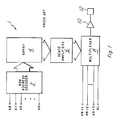
- Figure 1 is a schematic diagram of a simplified prior art random access memory array.
- Figures 2A through 2C are schematic diagrams of the decoding multiplexor.
- Figures 3A through 3E constitute a timing diagram illustrating the problems created by timing errors in the prior art circuits of Figures 2A through 2C.
- Figures 4A and 4B are schematic diagrams illustrating one embodiment of the present invention which solves the problems illustrated in Figures 1 through 3.
- Figures 5A through 5E constitute a timing diagram illustrating the operation of the embodiment of Figure 4A and 4B.
- FIG. 1 is a schematic diagram of a prior art RAM 1.
- RAM 1 receives address input signals via address terminals A0 through AL.
- the signals provided on address terminals A0 through AN drive row address decoder 2.
- row decoder provides signals to array 4 which selects a row of memory cells in array 4.
- the signals in the selected memory cells are provided to sense amplifiers 6 which receive the small signals provided from the memory cells, amplify them to full logic levels (usually 0 Volts for a logical 0 and 5 Volts for a logical 1) and 'latch' or store the signals.
- the latched row of signals is provided to multiplexor 8.
- Multiplexor 8 selects one of the bits in the stored row of data in response to the address signals provided via address terminals AN+1 through AL.
- the selected bit is provided to output buffer 10 which provides the selected bit on output terminal 12.
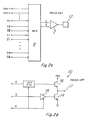
- Figures 2A through 2C are schematic diagrams detailing the column select circuitry of RAM 1 of Figure 1.
- the data bits are provided to multiplexor 8 in complementary form via terminals D0 through DM and D0 through DM .
- Multiplexor 8 selects one data bit and provides the selected data bit in complementary form on leads O and O .
- Multiplexor 8 selects the provided data bit in response to address signals provided on address terminals AN+1 through AL.
- the output data bit is provided to output buffer 10 which in turn provides the data bit to output pad 12.
- Output buffer 10 is enabled by a signal provided on input terminal E.
- FIG. 2B is a schematic diagram of output buffer 10 of Figures 1 and 2A.
- N-channel field effect transistors 14 and 16 drive output terminal 17.
- the gate of transistor 14 is driven by the signal provided on terminal O through buffer 18.
- buffer 18 For example, if a logical 0 is provided on terminal O, a complementary 1 is provided on terminal O , through buffer 18 to the gate of transistor 14.
- transistor 14 conducts and pulls down output terminal 17 to provide a logical 0 on terminal 17.
- a logical 1 is provided on terminal O
- a logical 0 is provided to the gate of transistor 14 through buffer 18 and thus transistor 14 does not pull down terminal 17.
- buffer 18 provides a logical 0 signal to the gate of transistor 14 and transistor 14 does not pull down the signal on terminal 17 regardless of the signal on terminal O.
- Transistor 16 is driven by booster circuit 20.
- N-channel transistor 16 is used instead of a P-channel transistor to avoid latch-up problems.
- V th threshold voltage
- boosting circuit 20 provides a signal to the gate of transistor 16 which is more than one V th greater than V dd (boosted signal).
- the signal on terminal O is a logical 1
- boosting circuit 20 provides a boosted signal and transistor 16 pulls up the signal on terminal 17 to V dd .
- boosting circuit 20 When the signal on terminal O is a logical 0, boosting circuit 20 provides a logical 0 and transistor 16 does not pull up the signal on terminal 17. When a signal indicating that buffer 10 should be disabled is received on terminal E, boosting circuit 20 provides a logical 0 output signal and transistor 16 does not pull up the signal on terminal 17 regardless of the signal on terminal O.
- Figure 2C is a schematic diagram of boosting circuit 20 of Figure 2B. Many types of boosting circuits are used in the art. Figure 2C illustrates one example of a boosting circuit.
- AND gate 22 provides an output signal of 0.
- the output signal of AND gate 22 is inverted once by invertor 24 and inverted back by invertor 26.
- the output signal of AND gate 22 is also inverted once by invertor 30, inverted back by invertor 32 and inverted again by invertor 34.
- invertor 34 provides a logical 1 or a signal of V dd .
- transistor 38 Because the gate of transistor 38 is tied to V dd , the drain of transistor 38, and thus the gate of transistor 28, is pulled to V dd less V th . This voltage causes transistor 28 to be on which pulls terminal 40 to 0 Volts. Thus the voltage provided by boosting circuit 20 is low and transistor 16 ( Figure 2B) does not conduct.
- Boosting circuit 20 develops the charge to provide a boosted voltage signal during the transition from a low voltage output signal to a high voltage boosted output signal.
- a logical 1 signal is provided on terminal E and the signal on terminal O changes from a logical 0 to a logical 1
- the positive charge accumulated on the plate of capacitor 42 connected to the gate of transistor 28 boosts the voltage on the gate of transistor 28 to greater than V dd .
- the positive charge was accumulated while the plate of capacitor 42 connected to the output terminal of AND gate 22 was held a 0 volts and the plate of capacitor 42 connected to the gate of transistor 28 was held at V dd less V th .
- Capacitor 42 must be a relatively small capacitance device to avoid over charging of the gate of transistor 28 and thereby destroying the gate insulator of transistor 28.
- the internal delays of invertors 24 and 26 allow time for capacitor 42 to dump charge onto the gate of transistor 28.
- the gate of transistor 28 is boosted to at least V dd plus V th . Therefore a full V dd is provided to terminal 40 through transistor 28.
- the V dd voltage level on terminal 40 also charges the plate of capacitor 44 connected to terminal 40 with a positive charge.
- the plate of capacitor 40 connected to the output terminal of invertor 36 is, at this time, held to 0 Volts.
- the logical 1 on the input terminal of invertor 30 propagates through invertors 30, 32 and 34 to provide a logical 0 to the source of transistor 38.
- This logical 0 voltage level causes the gate of transistor 28 to be pulled low through transistor 38. Thus transistor 28 ceases to conduct.
- the signal on the output terminal of invertor 36 goes from a logical 0 level to a logical 1 or V dd level. This causes the positive charge on the plate of capacitor 44 which is connected to terminal 40 to dump charge on to terminal 40.
- Capacitor 44 is selected to have a very large capacitance relative to the gate capacitance of transistor 16 ( Figure 2B) and the charge cannot be discharged through transistor 28, which is not conducting, so the voltage level on the gate of transistor 16 ( Figure 2B) is boosted well above V dd .
- Transistors 46, 48 and 50 are all gate strapped to the drain, which is connected away from V dd , and connected in series. Therefore, these transistors will begin to conduct if the voltage on terminal 40 rises to greater than 3 times V th above V dd . This limits the voltage on terminal 40 thereby avoiding damage to transistor 16 ( Figure 2B).
- Figures 3A through 3E are timing diagrams illustrating the problems caused by timing errors in the circuit of Figure 1 and Figures 2A through 2C.
- the timing diagrams of Figures 3A through 3E show the operation of a greatly simplified version of this circuit.
- N is equal to 0 and L is equal to 2. Therefore the array 4 ( Figure 1) includes 1 row and no row address signals are required.
- Figure 3A represents the address signal on address terminal A1 and Figure 3B represents the address signal on terminal A2. Because two binary bits can address four addresses, the row of storage elements includes 4 memory cells.
- Figure 3C shows the signal provided on terminal O ( Figure 2A) by multiplexor 8 in response to the signals shown in Figures 3A and 3B and the stored data shown in the table above.
- the address signals provided indicate that the data stored at position 0-1 is to be provided and thus a logical 1 is placed on terminal O.
- multiplexor 8 temporarily provides the data stored at position 0-0. This shows up as a downward spike in the signal provided on terminal O.
- FIG. 3D is a timing diagram of the signal provided on terminal 17 ( Figure 2B).
- output buffer 10 provides a full V dd output signal on terminal 17 because boosting circuit 20 boosts the voltage on the gate of transistor 16 ( Figure 2B) well above V dd plus V th .
- boosting circuit 20 receives the spike, the 'temporary' logical 0 propagates through boosting circuit 20 to provide a logical 0 on the output terminal of invertor 26. The logical 0 also propagates through to cause a logical 1 on the output terminal of invertor 34.
- FIG. 3E is a timing diagram showing the desired output signal on terminal 17.
- Figures 4A and 4B are schematic diagrams of one embodiment of the present invention designed to alleviate the spikes illustrated above in conjunction with Figures 1, 2A through 2C and Figures 3A through 3E.
- the embodiment of Figures 4A and 4B illustrate the example of the present invention with regard to column demultiplexion of data stored in a random access memory device.
- this one embodiment is described herein, the specific embodiment is not to be construed in any way as limiting the scope of the invention.
- the present invention finds broad applicability in any combinatorial logic or other type of circuit accepting two or more input signals and providing an output signal in response thereto.
- Figure 4A is a schematic diagram of one embodiment of the present invention.
- Multiplexor 8, buffer 10 and output terminal 12 operate in the same manner as similarly numbered components in Figure 2A.
- the circuit of Figure 4A further includes transition detector 52. Enable signals are often provided externally to the chip or generated on chip in response to other signals. In this embodiment, this signal is provided to the circuit of Figure 4A via terminal 56.
- the address signals provided on address terminals An+1 through AL are provided to transition detector 52.
- Transition detector 52 provides an output signal on terminal T which is a logical 1 when no transition has been detected and a logical 0 when a transition is detected.
- AND gate 54 provides a logical 1 to output buffer 10 and output buffer 10 provides an output signal to terminal 12 dependent on the signal provided on terminals O and O . If the enable signal on terminal 56 or the output signal of transition detector 52 is logical 0, output buffer 10 is disabled an provides a high impedance to terminal 12.
- a schematic diagram of a portion of transition detector 52 is shown in Figure 4B.
- the portion shown in Figure 4B operates on one input signal provided on terminal IN. If multiple input signals are to processed by transition detector 52, one of each of the circuits shown in Figure 4B must be provided and the output signals of the multiple circuits, provided on terminal OUT, must be combined by a AND gate such as AND gate 58.
- Single input transition detector 52A operates by providing a temporary transition detect signal of logical 0, in response to a detected transition, on terminal OUT of a duration set by delay unit 60.
- transistors 62, 64, 66, 68, 70, 72, 74 and 76 are assumed to be pure switching devices. Therefore, when one of these transistors is said to 'on' it means the transistor channel is conducting. Conversely, when a transistor is said to be 'off' it means the transistor channel is not conducting.
- a logical 0 signal is provided on terminal IN
- P-channel transistor 66 is on and N-channel transistor 64 is off.
- the signal on IN is inverted by invertor 78 and the output signal of logical 1 causes P-channel transistor 72 to be off and N-channel transistor 74 to be on.
- a logical 1 signal is provided to the gate of P-channel transistor 70 and the gate of N-channel transistor 62.
- transistor 70 is off and transistor 62 is on.
- the logical 1 provided to the input terminal of invertor 80 is inverted to provide a logical 0 on the gates of P-channel transistor 68 and N-channel transistor 76.
- transistor 68 is on and transistor 76 is off.
- the only path from terminal OUT to either V dd or ground is through transistors 66 and 68. Therefore, the signal provided on terminal OUT is V dd or a logical 1.
- partial transition detector 52A provides a logical 0 output signal after the transition from logical 0 to logical 1 of the signal on terminal IN for a period determined by the delay built into delay unit 60.
- the delay of delay unit 60 may be provided by any number of techniques, such as RC timing delays, multiple gate delays or clocked timing, for example.
- the logical 0 output signal of delay unit 60 is inverted by invertor 80 to provide a logical 1 on the gates of P-channel transistor 68 and N-channel transistor 76. Thus transistor 68 is off and transistor 76 is on.
- invertor 78 inverts the signal on terminal IN to provide a logical 1 on the gates of P-channel transistor 72 and N-channel transistor 74.
- transistor 72 turns off and transistor 74 turns on.
- Transistor 76 remains on until this logical 1 has propagated through delay unit 60 and invertor 80. Therefore, the path from terminal OUT to V dd is broken at transistor 72 and a path from terminal OUT through transistors 74 and 76 to ground is established. Thus a logical 0 output signal is provided on terminal OUT.
- the logical 0 on terminal IN causes P-channel transistor 66 to turn on and N-channel transistor 64 to turn off.
- invertor 80 inverts this signal to provide a logical 0 on the gates of P-channel transistor 68 and N-channel transistor 76.
- transistor 68 turns on and transistor 76 turns off. Therefore, the path from terminal OUT to ground is broken at transistor 76 and a path from terminal OUT through transistors 66 and 68 is established.
- a logical 1 is provided on terminal OUT.
- the logical 1 provided by delay unit 60 causes P-channel transistor 70 to turn off and N-channel transistor 62 to turn on. This brings partial transition detector 52A to the quiescent state with a logical 0 input signal as described above.
- partial transition detector 52A provides a logical 0 output signal of selected duration upon the transition of the signal provided on terminal IN from either a logical 0 to a logical 1 or from a logical 1 to a logical 0. Otherwise, partial transition detector provides a logical 1 output signal.
- the output signals of the partial transition detectors are provided as input signals to AND gate 58.
- all the input signals to AND gate 58 are logical 1 and the output signal of AND gate 58 is a logical 1. If any of the partial transition detectors detects a transition, one of the input signals to AND gate 58 is a logical 0 and the output signal of AND gate 58 is a logical 0.
- Figures 5A through 5C are the same a Figures 3A through 3C and describe the same signals.
- the signals shown in Figures 5A and 5B are provided to transition detector 52 and the output of transition detector 52 is shown in Figure 5D.
- transition detector 52 provides a logical 0 signal to AND gate 54 which then provides a logical 0 to enable terminal E of buffer 10.
- the logical 0 enable signal causes boosting circuit 20 ( Figure 2C) to provide a logical on terminal 40 ( Figure 2C). This causes capacitor 44 ( Figure 2C) to discharge.
- transition detector 52 is selected to be long enough to allow capacitor 44 to charge and thus allow boosting circuit 20 to operate normally.
- output buffer 10 is disabled and the output signal of output buffer 10 is suppressed.
- output buffer 10 is providing a high impedance output signal, the time periods involved are so short that the signal on terminal 12 does not change while the output signal of buffer 12 is suppressed. This is reflected in Figure 5E.
- output buffer 10 provides the spikeless output signal shown in Figure 5E on output terminal 12, By blocking the downward spike, the present embodiment allows boosting circuit 20 to properly charge, thus providing a full V dd output signal during time period t2 unlike the prior art signal shown in Figure 3D.
- the disable signal may be provided directly to the combinatorial circuit or to circuitry interposed between multiplexor 8 and output buffer 10. Any of these embodiments are design choices which are clearly within the scope of the present invention.
Landscapes
- Engineering & Computer Science (AREA)
- Physics & Mathematics (AREA)
- Computer Hardware Design (AREA)
- Nonlinear Science (AREA)
- Microelectronics & Electronic Packaging (AREA)
- Computing Systems (AREA)
- General Engineering & Computer Science (AREA)
- Mathematical Physics (AREA)
- Logic Circuits (AREA)
- Dram (AREA)
Claims (11)
- Circuit pour réaliser une opération combinatoire en réponse à au moins deux signaux d'entrée logiques, comprenant:- un circuit combinatoire (2, 4, 6, 8) pour recevoir lesdits signaux d'entrée, ledit circuit combinatoire (2, 4, 6, 8) fournissant un signal de sortie en réponse auxdits signaux d'entrée;- un détecteur de transition (52) pour recevoir une partie ou la totalité desdits signaux d'entrée, ledit détecteur de transition (52) fournissant un signal d'invalidation en réponse à une transition détectée sur l'un desdits signaux d'entrée reçus; et- un circuit de tampon de sortie (10) pour recevoir ledit signal de sortie, le circuit de tampon de sortie (10) fournissant un signal de sortie du circuit de tampon en réponse audit signal de sortie, ledit circuit de tampon de sortie (10) étant adapté pour recevoir ledit signal d'invalidation et ledit circuit de tampon de sortie (10) étant invalidé en réponse audit signal d'invalidation, caractérisé en ce que ledit circuit combinatoire reste fonctionnel et en ce qu'une variation brusque de retard se produisant dans une sortie du circuit combinatoire (0,
0 ) est supprimée par ledit circuit de tampon de sortie (10). - Circuit selon la revendication 1 dans lequel ledit circuit de tampon de sortie (10) comporte des transistors (14, 16) entre des conducteurs de courant fournissant ladite sortie du circuit de tampon.
- Circuit selon la revendication 2 dans lequel lesdits transistors (14, 16) sont des dispositifs à canal -n.
- Circuit selon l'une des revendications 2 et 3 dans lequel lesdits transistors fournissent une ligne de sortie (17) d'excursion haute ou basse.
- Circuit selon l'une quelconque des revendications 1, 3 et 4 comportant un circuit d'augmentation de de tension (20) relié à au moins un desdits transistors de sortie (14, 16), ledit circuit d'augmentation de tension (20) comportant un circuit de charge pour accumuler une charge pendant une certaine durée pour augmenter la tension dudit au moins un transistor de sortie jusqu'à une tension de sortie désirée.
- Circuit selon la revendication 5 dans lequel ledit circuit de charge comporte un condensateur (42) pour accumuler ladite charge.
- Circuit selon l'une des revendications 5 et 6 dans lequel ledit circuit de charge accumule la charge pendant une certaine durée suffisante pour augmenter la tension dudit au moins un transistor de sortie (14, 16) pour conduire au moins la tension audit conducteur de courant.
- Circuit selon l'une quelconque des revendications 2 à 7 dans lequel ledit détecteur de transition (52) comporte un premier ensemble de transistors (64, 66) relié pour recevoir un desdits signaux d'entrée, un second ensemble de transistors (72, 74) relié entre lesdits conducteurs de courant et ledit premier ensemble de transistors (64, 66) et un circuit de retard (60) adapté pour relier ledit second ensemble de transistors (72, 74) audit premier ensemble de transistors pour retarder le fonctionnement dudit premier ensemble de transistors (64, 66).
- Circuit selon la revendication 5 ou selon l'une quelconque des revendications 6 à 8 dépendantes de la revendication 5 comportant un circuit logique (30, 32, 34, 36) pour décharger la charge accumulée chaque fois que se produit une transition d'entrée.
- Circuit selon l'une quelconque des revendications précédentes dans lequel ledit signal d'invalidation est disponible en tant que première entrée (T) à une porte (54), ladite porte comportant une seconde entrée (56) pour recevoir un second signal d'invalidation.
- Circuit selon l'une quelconque des revendications précédentes dans lequel ledit circuit combinatoire est un circuit de décodage pour un dispositif à mémoire.
Applications Claiming Priority (2)
| Application Number | Priority Date | Filing Date | Title |
|---|---|---|---|
| US24519788A | 1988-09-16 | 1988-09-16 | |
| US245197 | 1988-09-16 |
Publications (3)
| Publication Number | Publication Date |
|---|---|
| EP0361233A2 EP0361233A2 (fr) | 1990-04-04 |
| EP0361233A3 EP0361233A3 (en) | 1990-06-20 |
| EP0361233B1 true EP0361233B1 (fr) | 1994-11-23 |
Family
ID=22925701
Family Applications (1)
| Application Number | Title | Priority Date | Filing Date |
|---|---|---|---|
| EP89117106A Expired - Lifetime EP0361233B1 (fr) | 1988-09-16 | 1989-09-15 | Circuit de suppresion de parasites |
Country Status (4)
| Country | Link |
|---|---|
| EP (1) | EP0361233B1 (fr) |
| JP (1) | JP3077808B2 (fr) |
| KR (1) | KR0150632B1 (fr) |
| DE (1) | DE68919459T2 (fr) |
Families Citing this family (3)
| Publication number | Priority date | Publication date | Assignee | Title |
|---|---|---|---|---|
| DE69030575T2 (de) * | 1990-06-29 | 1997-11-13 | Philips Electronics Nv | Integrierte Halbleiterschaltung mit einem Detektor |
| US5235602A (en) * | 1991-06-11 | 1993-08-10 | International Business Machines Corporation | Synchronous/asynchronous i/o channel check and parity check detector |
| US6718523B2 (en) | 2001-07-05 | 2004-04-06 | International Business Machines Corporation | Reduced pessimism clock gating tests for a timing analysis tool |
Family Cites Families (2)
| Publication number | Priority date | Publication date | Assignee | Title |
|---|---|---|---|---|
| US4337525A (en) * | 1979-04-17 | 1982-06-29 | Nippon Electric Co., Ltd. | Asynchronous circuit responsive to changes in logic level |
| JPS5963094A (ja) * | 1982-10-04 | 1984-04-10 | Fujitsu Ltd | メモリ装置 |
-
1989
- 1989-09-12 KR KR1019890013258A patent/KR0150632B1/ko not_active Expired - Lifetime
- 1989-09-14 JP JP01237406A patent/JP3077808B2/ja not_active Expired - Fee Related
- 1989-09-15 DE DE68919459T patent/DE68919459T2/de not_active Expired - Fee Related
- 1989-09-15 EP EP89117106A patent/EP0361233B1/fr not_active Expired - Lifetime
Also Published As
| Publication number | Publication date |
|---|---|
| KR0150632B1 (ko) | 1998-12-01 |
| JP3077808B2 (ja) | 2000-08-21 |
| KR900005475A (ko) | 1990-04-14 |
| EP0361233A3 (en) | 1990-06-20 |
| JPH02210914A (ja) | 1990-08-22 |
| EP0361233A2 (fr) | 1990-04-04 |
| DE68919459D1 (de) | 1995-01-05 |
| DE68919459T2 (de) | 1995-03-30 |
Similar Documents
| Publication | Publication Date | Title |
|---|---|---|
| US4965474A (en) | Glitch suppression circuit | |
| US5278789A (en) | Semiconductor memory device with improved buffer for generating internal write designating signal and operating method thereof | |
| US4647797A (en) | Assist circuit for improving the rise time of an electronic signal | |
| EP0624878A2 (fr) | Circuit intégré à semi-conducteurs | |
| US6081460A (en) | Integrated circuit devices having voltage level responsive mode-selection circuits therein and methods of operating same | |
| EP0887935B1 (fr) | Circuit d'isolation aux bruits | |
| US5124585A (en) | Pulsed bootstrapping output buffer and associated method | |
| JPH06150666A (ja) | 入力回路 | |
| US6825691B1 (en) | Apparatus and method for a radiation resistant latch with integrated scan | |
| EP0361233B1 (fr) | Circuit de suppresion de parasites | |
| US5170072A (en) | Buffer device having a booster circuit for a semiconductor memory device | |
| US5834949A (en) | Bus driver failure detection system | |
| EP0560623B1 (fr) | Mémoire à semi-conducteurs | |
| EP0105757B1 (fr) | Dispositif de mémoire semi-conductrice asynchrone | |
| EP0809249B1 (fr) | Circuit d'entrée pour mémoire à semi-conducteur | |
| EP0170781B1 (fr) | Dispositif de mémoire MOS dynamique | |
| US5901098A (en) | Ground noise isolation circuit for semiconductor memory device and method thereof | |
| EP0333206A2 (fr) | Circuit intégré à semi-conducteurs | |
| KR100233331B1 (ko) | 신호천이검출회로 | |
| JP2900941B2 (ja) | 半導体装置 | |
| US5323359A (en) | Semiconductor memory device | |
| US6542011B2 (en) | Driver circuit, receiver circuit, and semiconductor integrated circuit device | |
| US6169423B1 (en) | Method and circuit for regulating the length of an ATD pulse signal | |
| US6075718A (en) | Method and device for reading a non-erasable memory cell | |
| KR0179913B1 (ko) | 출력 인에이블 신호 발생 회로 |
Legal Events
| Date | Code | Title | Description |
|---|---|---|---|
| PUAI | Public reference made under article 153(3) epc to a published international application that has entered the european phase |
Free format text: ORIGINAL CODE: 0009012 |
|
| AK | Designated contracting states |
Kind code of ref document: A2 Designated state(s): DE FR GB IT NL |
|
| PUAL | Search report despatched |
Free format text: ORIGINAL CODE: 0009013 |
|
| AK | Designated contracting states |
Kind code of ref document: A3 Designated state(s): DE FR GB IT NL |
|
| 17P | Request for examination filed |
Effective date: 19901217 |
|
| 17Q | First examination report despatched |
Effective date: 19920814 |
|
| GRAA | (expected) grant |
Free format text: ORIGINAL CODE: 0009210 |
|
| ITF | It: translation for a ep patent filed | ||
| AK | Designated contracting states |
Kind code of ref document: B1 Designated state(s): DE FR GB IT NL |
|
| REF | Corresponds to: |
Ref document number: 68919459 Country of ref document: DE Date of ref document: 19950105 |
|
| ET | Fr: translation filed | ||
| PLBE | No opposition filed within time limit |
Free format text: ORIGINAL CODE: 0009261 |
|
| STAA | Information on the status of an ep patent application or granted ep patent |
Free format text: STATUS: NO OPPOSITION FILED WITHIN TIME LIMIT |
|
| 26N | No opposition filed | ||
| REG | Reference to a national code |
Ref country code: GB Ref legal event code: IF02 |
|
| PGFP | Annual fee paid to national office [announced via postgrant information from national office to epo] |
Ref country code: GB Payment date: 20060804 Year of fee payment: 18 |
|
| PGFP | Annual fee paid to national office [announced via postgrant information from national office to epo] |
Ref country code: NL Payment date: 20060807 Year of fee payment: 18 |
|
| PGFP | Annual fee paid to national office [announced via postgrant information from national office to epo] |
Ref country code: FR Payment date: 20060906 Year of fee payment: 18 |
|
| PGFP | Annual fee paid to national office [announced via postgrant information from national office to epo] |
Ref country code: DE Payment date: 20060929 Year of fee payment: 18 |
|
| PGFP | Annual fee paid to national office [announced via postgrant information from national office to epo] |
Ref country code: IT Payment date: 20060930 Year of fee payment: 18 |
|
| GBPC | Gb: european patent ceased through non-payment of renewal fee |
Effective date: 20070915 |
|
| PG25 | Lapsed in a contracting state [announced via postgrant information from national office to epo] |
Ref country code: NL Free format text: LAPSE BECAUSE OF NON-PAYMENT OF DUE FEES Effective date: 20080401 |
|
| NLV4 | Nl: lapsed or anulled due to non-payment of the annual fee |
Effective date: 20080401 |
|
| PG25 | Lapsed in a contracting state [announced via postgrant information from national office to epo] |
Ref country code: DE Free format text: LAPSE BECAUSE OF NON-PAYMENT OF DUE FEES Effective date: 20080401 |
|
| REG | Reference to a national code |
Ref country code: FR Ref legal event code: ST Effective date: 20080531 |
|
| PG25 | Lapsed in a contracting state [announced via postgrant information from national office to epo] |
Ref country code: FR Free format text: LAPSE BECAUSE OF NON-PAYMENT OF DUE FEES Effective date: 20071001 |
|
| PG25 | Lapsed in a contracting state [announced via postgrant information from national office to epo] |
Ref country code: GB Free format text: LAPSE BECAUSE OF NON-PAYMENT OF DUE FEES Effective date: 20070915 |
|
| PG25 | Lapsed in a contracting state [announced via postgrant information from national office to epo] |
Ref country code: IT Free format text: LAPSE BECAUSE OF NON-PAYMENT OF DUE FEES Effective date: 20070915 |