EP0361370A2 - Lecteur de carte à circuit intégré - Google Patents
Lecteur de carte à circuit intégré Download PDFInfo
- Publication number
- EP0361370A2 EP0361370A2 EP89117691A EP89117691A EP0361370A2 EP 0361370 A2 EP0361370 A2 EP 0361370A2 EP 89117691 A EP89117691 A EP 89117691A EP 89117691 A EP89117691 A EP 89117691A EP 0361370 A2 EP0361370 A2 EP 0361370A2
- Authority
- EP
- European Patent Office
- Prior art keywords
- contact
- spring
- detent means
- leg
- springs
- Prior art date
- Legal status (The legal status is an assumption and is not a legal conclusion. Google has not performed a legal analysis and makes no representation as to the accuracy of the status listed.)
- Granted
Links
Images


Classifications
-
- H—ELECTRICITY
- H01—ELECTRIC ELEMENTS
- H01R—ELECTRICALLY-CONDUCTIVE CONNECTIONS; STRUCTURAL ASSOCIATIONS OF A PLURALITY OF MUTUALLY-INSULATED ELECTRICAL CONNECTING ELEMENTS; COUPLING DEVICES; CURRENT COLLECTORS
- H01R12/00—Structural associations of a plurality of mutually-insulated electrical connecting elements, specially adapted for printed circuits, e.g. printed circuit boards [PCB], flat or ribbon cables, or like generally planar structures, e.g. terminal strips, terminal blocks; Coupling devices specially adapted for printed circuits, flat or ribbon cables, or like generally planar structures; Terminals specially adapted for contact with, or insertion into, printed circuits, flat or ribbon cables, or like generally planar structures
- H01R12/70—Coupling devices
- H01R12/71—Coupling devices for rigid printing circuits or like structures
- H01R12/72—Coupling devices for rigid printing circuits or like structures coupling with the edge of the rigid printed circuits or like structures
- H01R12/721—Coupling devices for rigid printing circuits or like structures coupling with the edge of the rigid printed circuits or like structures cooperating directly with the edge of the rigid printed circuits
-
- H—ELECTRICITY
- H01—ELECTRIC ELEMENTS
- H01R—ELECTRICALLY-CONDUCTIVE CONNECTIONS; STRUCTURAL ASSOCIATIONS OF A PLURALITY OF MUTUALLY-INSULATED ELECTRICAL CONNECTING ELEMENTS; COUPLING DEVICES; CURRENT COLLECTORS
- H01R13/00—Details of coupling devices of the kinds covered by groups H01R12/70 or H01R24/00 - H01R33/00
- H01R13/02—Contact members
- H01R13/26—Pin or blade contacts for sliding co-operation on one side only
Definitions
- This invention relates generally to a contact spring and, more particularly, to a set of biased contact springs.
- the invention further relates to a chipcard reader using said set of contact springs.
- the said set of contact springs can also be used as a connector specifically for flexible printed circuits.
- a large variety of different types of contact springs as well as sets of contact springs are known.
- Sets of contacts springs for contacting the contact areas of chipcards are known, for instance, from the German laid-open applications 35 31 318.8 and 36 02 668.9.
- the sets of contact elements for chipcards have to be designed such that the wear of the contact areas of the chipcards as well as the wear of the contact springs is kept small. For that reason, for the purposes of contacting, either the chipcard is pivoted towards a stationary set of contact elements or, reversely, a set of contact elements is pivoted towards the contact areas of a stationary chipcard.
- Such designs of so called chipcard readers handle the contact springs and the contact areas carefully, but they are complicated and thus expensive to manufacture. Moreover, the complicated design can cause mechanical as well as electrical problems.
- the present invention is directed to overcoming one or more of the problems as set forth above.
- the contact springs are of such a design that they can be used together with a contact support into which a plurality of contact springs is simultaneously inserted and mounted in accordance with the so-called "comb assembly technique".
- the comb assembly technique is a method according to which a plurality of contact springs, still attached to a common support strip, are simultaneously inserted and locateed in the contact support.
- the contact support is preferably a single piece component.
- the contact springs are biased after they are inserted into said contact support such that the spring characteristic starts with values F of the force being larger than zero.
- a contact spring which provides for a sliding contacting engagement and can be readily inserted with bias into a contact support, so as to form a set of contact elements.
- a chipcard reader is provided using a contact support into which contact springs are inserted, so that they are, after insertion, biased.
- the set of contact elements as well as the contact spring can be used in a connector for printed circuits, specifically flexible printed circuits.
- the invention will be described in connection with certain embodiments used for contacting the contact areas of a chipcard. However, the invention can also be used in different areas of contacting, for instance, in connection with a connector for a flexible printed circuit.
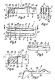
- Fig. 1 shows schematically in a perspective representation a set 1 of contact springs 2 adapted to contact the contact areas of a chipcard 3.
- the set 1 of contact elements 2 will be called a "contact set” 1 i.e. a row of contacts 2 which are somehow mounted in a contact support 5.
- the contact support 5, in turn, could form part of a chipcard reader.
- the chipcard reader would allow the proper insertion of the chipcard 3 for bringing the (not shown) contact areas of the chipcard 3 into contact with the contact springs 2.
- the contact set 1 is adapted to be connected with some apparatus, for instance, a telephone, which will make use of the data read from the chip of the chipcard 3.
- the lower ends of the contact springs 2 are connected for said purpose in a well-known manner to said apparatus 4.
- Fig. 1 shows schematically not only the spring contacts 2 of the first embodiment of the invention, but also refers to the spring contacts 200 of a second embodiment of the invention.
- Fig. 1 refers to guide grooves 14 of the first embodiment as well as guide grooves 140 of the second embodiment, both said grooves will be described later.
- the contact support 5 of Fig. 1 comprises an upper wall 6, a side wall 7, a front wall 8 and another (right) side wall 9 as well as a rear wall 13.
- each contact spring 2 preferably, however, a plurality of contact springs 2 are mounted.
- guide grooves 14 are provided, adapted to receive contact springs 2.
- Each of said guide grooves 14 comprises a narrow portion 15 as well as a wider portion 16.
- the wider portion 16 continues in the side wall 7, as can be seen in Fig. 4.
- Reference numeral 17 refers to the separating line between the narrower portion and the wider portion 16.
- the contact spring 2 is preferably a stamped resilient metal strip.
- the contact spring 2 comprises (see specifically Fig. 2), starting from the left, a termination portion 21 in the form of a solder termination portion. Then, continuing from the left in Fig. 2, the contact spring 2 comprises second detent means 22 in the form of a second tab section 22 formed by means of two tabs 23, 24 (see Fig. 4). Adjacent to said second tab section 22 an angular portion 28 (see Figs. 2 and 6) can be recognized, as well as adjacent thereto first detent means in the form of a first tab section 25, which comprises two tabs 26 and 27 (see Fig. 3).
- Adjacent to the first detent means 25 extends substantially in the X-direction (see Fig. 3) a longitudinal portion 28 which becomes a ramp portion 30 and a ramp portion 32 forming a cusp 31. Adjacent and to the right of cusp 31 the free end of the contact spring forms an abutment portion 33.
- the angle of ramp portion 30 is referred to by gamma.
- the termination portion 21 extends substantially in Y-direction.
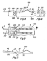
- the contact spring 2 is formed by two spring legs, a first spring leg 70 and a second spring leg 71.
- the leg 71 forms an angle of 90 ° with respect to the leg 70.
- the so-called angular portion 28 comprises a curved portion 73 and a straight portion 74.
- Fig. 7 discloses that the straight portion 74 and the straight longitudinal portion 29 are not located on one line, but form an angle alpha, smaller than 180°; for instance, alpha is 170°.
- the cusp shape of the contact spring (contact element) 2 forms a small ramp angle gamma which is, for instance, in the order of 30°, so that no deformation of the contact spring 2 occurs if the chipcard 3 comes into sliding engagement with said contact spring 2.
- Fig. 7 shows a contact spring 2 in its shape prior to the insertion into the contact support (housing) 5, while the other Figs. 2-6 show the contact spring 2 in its shape after insertion into the contact support 5.
- the contact spring 2 is symmetric with respect to center line 53 (see Fig. 3) and is located in the appropriate guide groove 14.
- the contact support 5 which is preferably of a one-piece design, will be explained.
- the contact elements 2 can be inserted in such a manner that they are fixedly mounted due to the above detent means, and they are also, after being properly inserted, biased so that the spring characteristic of a contact spring (contact element) 2 starts with a force F which is larger than zero.
- first counter detent means are provided in the form of two detent noses 43 at the contact support 5.
- the detent noses 42 are provided at a connecting member 38 of the contact support 5.
- Said first counter detent means 43 cooperate with the first detent means 25 of the contact spring 2.
- second counter detent means 42 are provided in the form of two detent noses 42 which again are provided at the contact support 5, particularly the connecting member 38 of said support 5.
- the noses 43 and 42 respectively, form detent surfaces which are offset with respect to each other by 90°.
- the second detent means 22 cooperate with said second counter detent means 42.
- the first and second tab sections 25 and 22 have substantially the same shape and a width 51 (see Fig. 4) which corresponds in substance to the width of the widened portion 16, but is naturally somewhat smaller, so that the contact springs can be inserted.
- the width 50 (see Fig. 4) of the contact springs 2 corresponds in substance to the width of the smaller portion 15 of the guide groove 14, but is naturally somewhat smaller than said width. Thus, a good guidance effect is provided for said contact springs 2.
- the assembly of the contact springs 2 is carried out in accordance with the so-called "comb assembly technique", i. e. a comb of contact springs 2 is used.
- a comb of contact springs is generated during the stamping process, after which the individual contact springs 2 are still an integral part of a metal strip connecting all said contact springs.
- This entire “comb” is placed on the contact support 5 such that initially the second detent means 22 are brought into engagement with the second counter detent means 42, whereupon then the contact springs 2 are slidably pressed along the inclined plane 40 up until the first detent means are inserted behind the first counter detent means 43, while at the same time the free ends of the springs, i. e.
- Figs. 8 through 11 disclose a second embodiment of the invention.
- the contact set is referred to by reference numeral 100 and the contact spring is referred to by reference numeral 200. Similar to the first embodiment, a contact support 500 is provided. The upper wall of the contact support is referred to by reference numeral 6 similar to Fig. 1.
- guide grooves 140 (referred to with reference numeral 14 in the first embodiment) are provided, which could also be called contact chambers.
- the contact springs 200 are located.
- the wider portion of the guide groove 140 is referred to by reference numeral 160 (see Fig. 9).
- an angular bar 36 provides abutment means for the free end or abutment portion 33 of the contact element 200.
- a connecting member 380 similar to contacting member 38 in the first embodiment, is provided but forms here only one counter detent means in the form of two detent noses 430. Similar to what was described in connection with Fig. 6 the second embodiment features a guide surface 400 similar to guide surface 40 of the first embodiment. Offset in upward and in leftward direction (see Fig. 8) with respect to the upper end of the connecting member 38, a cross member or abutment means 80 is provided, and the contact spring 200 is in contact with the bottom side of said contact means 80.
- the contact spring 200 is of a somewhat different design than the contact spring of Fig. 7.
- the first contact legs 70 of both springs 2 and 200 are of identical design, but the second leg 710 of the spring 200 is simply a straight portion 48 which does not possess a portion corresponding to the angular portion 28 of spring 2.
- the straight portion 48 is used as a termination portion.
- an angle alpha in the range of 170° is formed between the straight portion 48 and the longitudinal portion 29 of the first leg 70.
- the contact spring 200 comprises only first detent means in the form of a first detent section 25, said detent section 25 again comprising, similarly to contact spring 2, tabs 26 and 27.
- the tab section 25 is preferably located just in the longitudinal portion 29, so that the angular deflection about the angle alpha occurs only to the left (see Fig. 11) adjacent to the tab section 25.
- a contact spring 200 having an angle alpha of 180°.
- the arrangement of the cross bar 80 and of thebar 36 as well as of the upper abutment surface of the tab member 380 is selected such that the spring 200 is biased after being insered.
- the second embodiment discloses that the principle of a biased spring can also be used for a straight spring contact.
- the detent means 25 provide for abutment in both longitudinal directions instead of the noses 42, which provides for an opposing bearing means for creating the bias, the cross bar 80 is used in connection with the contact support 500.
- Fig. 12 discloses a third embodiment of a contact set 800 which comprises a contact support 806 and contact springs 801.
- Contact spring 801 is substantially similar to contact spring 200 shown in Fig. 11; i.e. in the position shown in Fig. 12 the contact spring 801 is in its biased condition.
- the abutment means 80 of Fig. 12 are similar to the abutment means 80 of Fig. 8, the same is true for the angular tab member 36.
- Connecting member 381 of Fig. 12 is of mirror-like design to the connecting member 380 of Fig. 8.
- the connecting member 381 comprises an abutment surface 382 located on the right-hand side of tabs 25 of the spring 801.
- Connecting member 381 further comprises guide surfaces 383 similar to the guide surfaces 400 of Figs. 8 and 9.
- the contact springs 801 are inserted from the right with the tabs 25 sliding along the ramp-shaped guide surfaces 383 until the tabs 25 come into engagement with the abutment surfaces 382.
- a contact spring consisting of a resilient metal strip and comprising: detent means (25, 22; 25) adapted to mount the contact spring in a contact support (5), and a first and a second spring leg (70, 71; 70, 710), said detent means (22) being provided at the transition between the first to the second spring leg, a contact cusp (31) formed by said first spring leg (70), and wherein said contact spring is adapted to be mounted in said contact support (5) in a biased condition.
- a contact spring comprising: a metal strip, detent means provided by said metal strip and adapted to locate said contact spring in a contact spring receiving contact support (5), a first and a second spring leg, wherein one of the spring legs forms an angle with respect to said other spring leg, detent means (22) provided in the area of the second spring leg and a contact cusp (31) formed by said first spring leg (70) adjacent to the free end of said first spring leg which forms an abutment portion (33).
- the spring of 1 wherein said first and second spring legs include an obtuse angle alpha. 4.
- the spring of 2 wherein in the area of said first spring leg (70) another detent means is provided. 5.
- the spring of 1 wherein it is of integral or one-piece design and has a form which is symmetric with respect to a center line (53). 6.
- the spring of 1 wherein said detent means is provided in the form of a tab section.
- each tab section comprises two tabs arranged symmetrically with respect to said center line.
- the contact spring of 2 wherein two tab sections are provided, a first tab section (25) and a second tab section (22), one tab section being formed in said first spring leg, while the second tab section is being formed in said second spring leg.
- the contact spring of wherein said contact springs are formed by stamping which leaves a connecting strip for a plurality of contact springs such that comb-like structures are formed which are adapted to be inserted into a contact support, whereupon said connecting strip is removed.
- the contact spring of 1 wherein said cusp comprises a small angle gamma of contact.
- the contact spring of 2 wherein the angle between said first and second leg is approximately 90°.
- the contact spring of 10 wherein said cusp is of symmetric design.
- the contact spring of 1 wherein said first spring leg forms an angle alpha of about 170° with respect to said second spring leg, in an unbiased condition.
- the contact spring of 10 wherein said angle alpha is approximately 175°.
- the contact spring of 1 wherein the width of the contact spring is approximately three times the thickness of the contact spring.
- the contact spring of 1 wherein the width of the contact spring in the area of the tab sections is about twice the width of the spring outside of said tab sections.
- said first and second detent means are of identical design.
- the contact spring of 1 wherein said second spring leg is of a straight line design and is formed by a straight portion (48).
- 20. The contact spring of 19 wherein the angle between the first and second spring legs (70, 710) about the angle alpha occurs adjacent to said tab section. 21.
- a set of contact elements comprising: a contact support, at least one, preferably a plurality of contact springs, said contact springs being fixedly mounted in said contact support by means of the "comb assembling technique", and wherein further said contact support is preferably of integral design. 22. The set of contact elements of 21 wherein said contact springs are biased after being mounted in said contact support. 23. The set of contact elements wherein said contact springs are designed as mentioned in 1. 24. The set of contact elements of 21 wherein said contact support comprises counter detent means adapted to cooperate with said detent means of said contact elements. 25. The set of contact elements of 24 wherein said counter detent means are spaced from each other (in X-direction) and are located at different levels (in Y-direction). 26.
- 27. The set of contact elements of 24 wherein the contact spring is inserted into said contact support in such a manner that the detent means of the contact springs are in positive engagement with said counter detent means.
- 28. The set of contact elements of 27 wherein said counter detent means are formed by noses (43, 42) of the contact support.
- 29. The set of contact elements of 28 wherein said noses are formed at a connecting member (18) of said contact support (5).
- 30. The set of contact elements of 24 wherein each of two counter detent means are formed by spaced apart noses. 31.
- the set of contact elements of 31 wherein said guide means have guide surfaces in the form of an inclined plane.
- the set of contact elements of 31 wherein the contact support (5) comprises for each contact element a guide groove, preferably arranged in the upper wall of the contact support and wherein said guide groove comprises a narrow portion and adjacent thereto a wide portion. 35.
- each contact element is tensioned between two points (80, 381) and are biased with respect to abutment means (36).
- 36. The set of contact elements of 21 wherein a connecting member is provided which forms counter detent means which cooperate with detent means of the contact spring.
- 37. The set of contact elements as set forth in 36 wherein said connecting member comprises guide surfaces in the form of inclined planes, so as to guide said detent means of the spring into the detent or rest position.
- said counter detent means are provided in the form of two detent noses.
- the set of contact elements as set forth in 23 wherein the bias of spring (200) in the mounted position is generated by providing an angle alpha between the first and second legs in the not yet mounted condition of the contact spring. 42.
Landscapes
- Coupling Device And Connection With Printed Circuit (AREA)
Applications Claiming Priority (2)
| Application Number | Priority Date | Filing Date | Title |
|---|---|---|---|
| DE3832588A DE3832588C2 (de) | 1988-09-24 | 1988-09-24 | Kontaktsatz |
| DE3832588 | 1988-09-24 |
Publications (3)
| Publication Number | Publication Date |
|---|---|
| EP0361370A2 true EP0361370A2 (fr) | 1990-04-04 |
| EP0361370A3 EP0361370A3 (en) | 1990-10-31 |
| EP0361370B1 EP0361370B1 (fr) | 1996-03-13 |
Family
ID=6363694
Family Applications (1)
| Application Number | Title | Priority Date | Filing Date |
|---|---|---|---|
| EP89117691A Expired - Lifetime EP0361370B1 (fr) | 1988-09-24 | 1989-09-25 | Lecteur de carte à circuit intégré |
Country Status (4)
| Country | Link |
|---|---|
| US (1) | US4975086A (fr) |
| EP (1) | EP0361370B1 (fr) |
| JP (1) | JP2863211B2 (fr) |
| DE (1) | DE3832588C2 (fr) |
Cited By (2)
| Publication number | Priority date | Publication date | Assignee | Title |
|---|---|---|---|---|
| EP0735616A3 (fr) * | 1995-03-31 | 1997-03-19 | Wieland Elektrische Industrie | Connecteur électrique, notamment pour des plaquettes de circuits |
| EP0802582A3 (fr) * | 1996-04-18 | 1998-12-30 | Valeo Electronics Verwaltung GmbH | Dispositif de contact |
Families Citing this family (34)
| Publication number | Priority date | Publication date | Assignee | Title |
|---|---|---|---|---|
| US5369259A (en) * | 1989-09-21 | 1994-11-29 | Amphenol Corporation | Chip card reader |
| DE3943703C2 (de) * | 1989-09-21 | 2001-06-21 | Amphenol Tuchel Elect | Chipkartenleser |
| DE4118312C2 (de) * | 1991-06-04 | 1995-03-09 | Amphenol Tuchel Elect | Kontaktsatz für eine Kontaktzonen aufweisende Karte |
| US5188534A (en) * | 1992-03-19 | 1993-02-23 | Molex Incorporated | Surface mount connector with clip engaging contacts |
| US5487684A (en) * | 1992-07-01 | 1996-01-30 | Berg Technology, Inc. | Electrical contact pin for printed circuit board |
| EP0698247B1 (fr) * | 1993-05-14 | 1998-09-02 | AMPHENOL-TUCHEL ELECTRONICS GmbH | Lecteur a montage en surface de cartes a module d'identification d'abonne et de cartes standard |
| EP0698248A1 (fr) * | 1993-05-14 | 1996-02-28 | AMPHENOL-TUCHEL ELECTRONICS GmbH | Systeme de contact et lecteur pour cartes a puces |
| US5896225A (en) * | 1993-05-24 | 1999-04-20 | Deutsche Thomson Brandt Gmbh | Device for stereoscopic image observation within an increased observation area |
| DE9407499U1 (de) * | 1994-05-05 | 1995-09-07 | Itt Composants Et Instruments, Dole Cedex | Elektrisches Kontaktelement |
| DE19502176A1 (de) * | 1995-01-25 | 1996-08-08 | Thomas & Betts Gmbh | Chipkarten-Lesegerät |
| DE19506606C2 (de) * | 1995-02-24 | 1996-12-19 | Amphenol Tuchel Elect | Chipkartenleser |
| DE19508363C1 (de) * | 1995-03-10 | 1996-07-25 | Amphenol Tuchel Elect | Aufnahmegehäuse für eine Chipkarte |
| DE19516987A1 (de) * | 1995-05-09 | 1996-11-14 | Amphenol Tuchel Elect | Kartenlesevorrichtung für Chipkarten und/oder SIM-Karten mit unterschiedlicher Dicke |
| FR2743464A1 (fr) * | 1996-01-10 | 1997-07-11 | Philips Electronics Nv | Appareil muni d'un boitier amovible contenant un adaptateur permettant la lecture de cartes a puces aux formats differents |
| FR2743463A1 (fr) * | 1996-01-10 | 1997-07-11 | Philips Electronics Nv | Appareil muni d'un adaptateur permettant la lecture de cartes a puces aux formats differents |
| US8033838B2 (en) * | 1996-02-21 | 2011-10-11 | Formfactor, Inc. | Microelectronic contact structure |
| DE19607738A1 (de) * | 1996-02-29 | 1997-09-11 | Whitaker Corp | Anordnung zur elektrischen Verbindung einer Chipkarte mit einer gedruckten Schaltungskarte |
| DE19611422C2 (de) * | 1996-03-22 | 2001-06-07 | Tyco Electronics Logistics Ag | Verbinder für die elektrische Verbindung von zwei Leiterplatten miteinander |
| DE19634565C1 (de) * | 1996-08-27 | 1997-11-06 | Amphenol Tuchel Elect | Kontaktträger |
| DE19638622A1 (de) * | 1996-09-20 | 1998-03-26 | Amphenol Tuchel Elect | Chipkarten-Kontaktiergerät |
| EP0840246B2 (fr) * | 1996-11-05 | 2011-03-16 | Amphenol-Tuchel Electronics GmbH | Dispositif de contact pour cartes SIM |
| US5975959A (en) * | 1996-12-17 | 1999-11-02 | The Whitaker Corporation | Smart card connector module |
| US6231395B1 (en) * | 1997-03-17 | 2001-05-15 | Framatome Connectors International | Card reader connector, with elastic brush contacts, and reader comprising same |
| DE19755715A1 (de) * | 1997-12-15 | 1999-06-24 | Amphenol Tuchel Elect | Chipkartenleser |
| JP3295715B2 (ja) * | 1997-12-26 | 2002-06-24 | 日本圧着端子製造株式会社 | プリント配線板用コネクタ及びその製造方法 |
| DE20010669U1 (de) * | 2000-06-21 | 2001-10-31 | ITT Manufacturing Enterprises, Inc., Wilmington, Del. | Elektrische Verbindungseinrichtung |
| US6438638B1 (en) | 2000-07-06 | 2002-08-20 | Onspec Electronic, Inc. | Flashtoaster for reading several types of flash-memory cards with or without a PC |
| US7295443B2 (en) | 2000-07-06 | 2007-11-13 | Onspec Electronic, Inc. | Smartconnect universal flash media card adapters |
| US6830474B2 (en) * | 2002-08-16 | 2004-12-14 | Carry Computer Eng Co. Ltd. | Common connector with embedded pins |
| JP4184251B2 (ja) * | 2003-12-17 | 2008-11-19 | 第一電子工業株式会社 | カードコネクタ |
| KR100711292B1 (ko) * | 2005-04-14 | 2007-04-25 | 한국과학기술원 | 프로브 카드 및 그 제조방법 |
| WO2007008654A2 (fr) * | 2005-07-13 | 2007-01-18 | Amphenol Corporation | Contact lga cylindrique |
| JP2014164884A (ja) * | 2013-02-22 | 2014-09-08 | Fujitsu Component Ltd | コネクタ |
| DE102016108319B4 (de) * | 2016-05-04 | 2018-08-02 | Amphenol-Tuchel Electronics Gmbh | Schaltfederanordnung |
Family Cites Families (14)
| Publication number | Priority date | Publication date | Assignee | Title |
|---|---|---|---|---|
| US3464054A (en) * | 1968-01-15 | 1969-08-26 | Sylvania Electric Prod | Electrical connector |
| US3676926A (en) * | 1970-05-20 | 1972-07-18 | Elfab Corp | Method for manufacturing connector terminals |
| US3737838A (en) * | 1971-11-17 | 1973-06-05 | Itt | Printed circuit board connector |
| GB1424882A (en) * | 1973-05-29 | 1976-02-11 | Plessey Co Ltd | Edge connector |
| US4274699A (en) * | 1978-04-27 | 1981-06-23 | E. I. Du Pont De Nemours And Company | Press fit terminal with spring arm contact for edgecard connector |
| US4288140A (en) * | 1979-12-20 | 1981-09-08 | Bell Telephone Laboratories, Incorporated | Printed wiring board interconnection apparatus |
| FR2564643A1 (fr) * | 1984-05-15 | 1985-11-22 | Francelco Sa | Contact pour cartes a circuits imprimes |
| JPS618982U (ja) * | 1984-06-21 | 1986-01-20 | 沖電気工業株式会社 | 基板接続機構 |
| JPS6111284U (ja) * | 1984-06-26 | 1986-01-23 | 沖電線株式会社 | 基板接続コネクタ |
| GB8510840D0 (en) * | 1985-04-29 | 1985-06-05 | Allied Corp | Electrical connectors |
| DE3546780C2 (de) * | 1985-09-02 | 1996-04-25 | Amphenol Corp | Kontaktiereinrichtung für eine Chipkarte |
| DE3602668A1 (de) * | 1986-01-29 | 1987-07-30 | Allied Corp | Kontaktiereinrichtung fuer eine chip-karte |
| US4698025A (en) * | 1986-09-15 | 1987-10-06 | Molex Incorporated | Low profile modular phone jack assembly |
| US4770639A (en) * | 1987-03-02 | 1988-09-13 | Switchcraft, Inc. | Channelized jackfield |
-
1988
- 1988-09-24 DE DE3832588A patent/DE3832588C2/de not_active Expired - Fee Related
-
1989
- 1989-09-22 JP JP1245345A patent/JP2863211B2/ja not_active Expired - Fee Related
- 1989-09-22 US US07/410,832 patent/US4975086A/en not_active Expired - Lifetime
- 1989-09-25 EP EP89117691A patent/EP0361370B1/fr not_active Expired - Lifetime
Cited By (2)
| Publication number | Priority date | Publication date | Assignee | Title |
|---|---|---|---|---|
| EP0735616A3 (fr) * | 1995-03-31 | 1997-03-19 | Wieland Elektrische Industrie | Connecteur électrique, notamment pour des plaquettes de circuits |
| EP0802582A3 (fr) * | 1996-04-18 | 1998-12-30 | Valeo Electronics Verwaltung GmbH | Dispositif de contact |
Also Published As
| Publication number | Publication date |
|---|---|
| JP2863211B2 (ja) | 1999-03-03 |
| DE3832588C2 (de) | 1994-06-01 |
| DE3832588A1 (de) | 1990-03-29 |
| US4975086A (en) | 1990-12-04 |
| JPH02121285A (ja) | 1990-05-09 |
| EP0361370B1 (fr) | 1996-03-13 |
| EP0361370A3 (en) | 1990-10-31 |
Similar Documents
| Publication | Publication Date | Title |
|---|---|---|
| EP0361370A2 (fr) | Lecteur de carte à circuit intégré | |
| EP0926769B1 (fr) | Connecteur électrique très mince pour connecter une carte à puce | |
| US5975959A (en) | Smart card connector module | |
| USRE33268E (en) | Chip carrier socket having improved contact terminals | |
| KR100666067B1 (ko) | 직교 접촉 아암 및 옵셋 접촉 영역을 갖는 전기 접촉자 | |
| US5997315A (en) | Connector and IC card connector | |
| US6299458B1 (en) | Intermediate electrical connector | |
| US6062871A (en) | Interconnecting electrical connector | |
| JPH0613117A (ja) | 電気コネクタ | |
| KR20010053402A (ko) | 스마트 카드 접속용 전기 커넥터 | |
| JPH1092526A (ja) | 接点支持体 | |
| EP0867055B1 (fr) | Connecteur de carte enfichable pour plaquette de circuit imprime | |
| US4984996A (en) | Printed circuit board edge connector | |
| EP0595025B1 (fr) | Assemblage d'un connecteur électrique et moyens d'éjection pour connecter des cartes de circuits intégrés sur des plaquettes de circuits imprimés | |
| JPH11250197A (ja) | 接点エレメント支持部 | |
| EP1349240B1 (fr) | Connecteur avec contact dont le mouvement pour part est guidé par isolant | |
| US5575663A (en) | Electrical connector for mounting to an edge of a circuit board | |
| US20030162416A1 (en) | Electrical connector of at least two-direction card insertion type | |
| KR100228457B1 (ko) | 접속 장치 | |
| US6431898B1 (en) | Card connector | |
| EP0849842A2 (fr) | Modul connecteur de carte à micro-circuit | |
| JP2619184B2 (ja) | エジェクタユニット | |
| US5827075A (en) | Assembly of an electrical connector and ejector unit for connecting IC cards to printed circuit boards | |
| EP0981103A1 (fr) | Connecteur pour cartes à puce ayant différentes épaisseurs | |
| JP2977125B2 (ja) | コネクタ |
Legal Events
| Date | Code | Title | Description |
|---|---|---|---|
| PUAI | Public reference made under article 153(3) epc to a published international application that has entered the european phase |
Free format text: ORIGINAL CODE: 0009012 |
|
| AK | Designated contracting states |
Kind code of ref document: A2 Designated state(s): BE FR GB IT NL SE |
|
| PUAL | Search report despatched |
Free format text: ORIGINAL CODE: 0009013 |
|
| AK | Designated contracting states |
Kind code of ref document: A3 Designated state(s): BE FR GB IT NL SE |
|
| 17P | Request for examination filed |
Effective date: 19910102 |
|
| 17Q | First examination report despatched |
Effective date: 19930923 |
|
| ITF | It: translation for a ep patent filed | ||
| GRAH | Despatch of communication of intention to grant a patent |
Free format text: ORIGINAL CODE: EPIDOS IGRA |
|
| GRAA | (expected) grant |
Free format text: ORIGINAL CODE: 0009210 |
|
| AK | Designated contracting states |
Kind code of ref document: B1 Designated state(s): BE FR GB IT NL SE |
|
| ET | Fr: translation filed | ||
| PLBE | No opposition filed within time limit |
Free format text: ORIGINAL CODE: 0009261 |
|
| STAA | Information on the status of an ep patent application or granted ep patent |
Free format text: STATUS: NO OPPOSITION FILED WITHIN TIME LIMIT |
|
| 26N | No opposition filed | ||
| PGFP | Annual fee paid to national office [announced via postgrant information from national office to epo] |
Ref country code: NL Payment date: 20000620 Year of fee payment: 12 |
|
| PGFP | Annual fee paid to national office [announced via postgrant information from national office to epo] |
Ref country code: GB Payment date: 20000807 Year of fee payment: 12 |
|
| PGFP | Annual fee paid to national office [announced via postgrant information from national office to epo] |
Ref country code: SE Payment date: 20000901 Year of fee payment: 12 |
|
| PGFP | Annual fee paid to national office [announced via postgrant information from national office to epo] |
Ref country code: BE Payment date: 20001010 Year of fee payment: 12 |
|
| PGFP | Annual fee paid to national office [announced via postgrant information from national office to epo] |
Ref country code: FR Payment date: 20010831 Year of fee payment: 13 |
|
| PG25 | Lapsed in a contracting state [announced via postgrant information from national office to epo] |
Ref country code: GB Free format text: LAPSE BECAUSE OF NON-PAYMENT OF DUE FEES Effective date: 20010925 |
|
| PG25 | Lapsed in a contracting state [announced via postgrant information from national office to epo] |
Ref country code: SE Free format text: LAPSE BECAUSE OF NON-PAYMENT OF DUE FEES Effective date: 20010926 |
|
| PG25 | Lapsed in a contracting state [announced via postgrant information from national office to epo] |
Ref country code: BE Free format text: LAPSE BECAUSE OF NON-PAYMENT OF DUE FEES Effective date: 20010930 |
|
| REG | Reference to a national code |
Ref country code: GB Ref legal event code: IF02 |
|
| BERE | Be: lapsed |
Owner name: AMPHENOL-TUCHEL ELECTRONICS G.M.B.H. Effective date: 20010930 |
|
| PG25 | Lapsed in a contracting state [announced via postgrant information from national office to epo] |
Ref country code: NL Free format text: LAPSE BECAUSE OF NON-PAYMENT OF DUE FEES Effective date: 20020401 |
|
| EUG | Se: european patent has lapsed |
Ref document number: 89117691.9 |
|
| GBPC | Gb: european patent ceased through non-payment of renewal fee |
Effective date: 20010925 |
|
| NLV4 | Nl: lapsed or anulled due to non-payment of the annual fee |
Effective date: 20020401 |
|
| NLV4 | Nl: lapsed or anulled due to non-payment of the annual fee |
Effective date: 20020401 |
|
| PG25 | Lapsed in a contracting state [announced via postgrant information from national office to epo] |
Ref country code: FR Free format text: LAPSE BECAUSE OF NON-PAYMENT OF DUE FEES Effective date: 20030603 |
|
| REG | Reference to a national code |
Ref country code: FR Ref legal event code: ST |
|
| PG25 | Lapsed in a contracting state [announced via postgrant information from national office to epo] |
Ref country code: IT Free format text: LAPSE BECAUSE OF NON-PAYMENT OF DUE FEES;WARNING: LAPSES OF ITALIAN PATENTS WITH EFFECTIVE DATE BEFORE 2007 MAY HAVE OCCURRED AT ANY TIME BEFORE 2007. THE CORRECT EFFECTIVE DATE MAY BE DIFFERENT FROM THE ONE RECORDED. Effective date: 20050925 |