EP0361801B1 - Interrupteur à semi-conducteur pour micro-ondes - Google Patents
Interrupteur à semi-conducteur pour micro-ondes Download PDFInfo
- Publication number
- EP0361801B1 EP0361801B1 EP89309660A EP89309660A EP0361801B1 EP 0361801 B1 EP0361801 B1 EP 0361801B1 EP 89309660 A EP89309660 A EP 89309660A EP 89309660 A EP89309660 A EP 89309660A EP 0361801 B1 EP0361801 B1 EP 0361801B1
- Authority
- EP
- European Patent Office
- Prior art keywords
- terminal
- directional coupler
- microwave
- switching elements
- transmission
- Prior art date
- Legal status (The legal status is an assumption and is not a legal conclusion. Google has not performed a legal analysis and makes no representation as to the accuracy of the status listed.)
- Expired - Lifetime
Links
Images

Classifications
-
- H—ELECTRICITY
- H04—ELECTRIC COMMUNICATION TECHNIQUE
- H04B—TRANSMISSION
- H04B1/00—Details of transmission systems, not covered by a single one of groups H04B3/00 - H04B13/00; Details of transmission systems not characterised by the medium used for transmission
- H04B1/38—Transceivers, i.e. devices in which transmitter and receiver form a structural unit and in which at least one part is used for functions of transmitting and receiving
- H04B1/40—Circuits
- H04B1/44—Transmit/receive switching
Definitions
- the present invention relates to a microwave transmit-receive switch, and more particularly to an improvement in a circuit construction of a transmit-receive switch (hereinafter referred to as "TR" switch) in microwave frequency band.
- TR transmit-receive switch
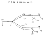
- Figure 2 shows a circuit construction of a prior art microwave transmit-receive switch.
- the microwave transmit-receive switch includes semiconductor switching elements 1a and 1b such as diode or transistor, a receiving terminal and transmission terminal 2 and 3, a common signal terminal 4 connected with an antenna, and quarter wavelength transmission lines 21 and 31 connecting the switching elements 1a and 1b and the branching point 5 where the line branches from the antenna terminal 4 to the transmission terminal 3 and the receiving terminal 2.
- semiconductor switching elements 1a and 1b such as diode or transistor
- receiving terminal and transmission terminal 2 and 3 a common signal terminal 4 connected with an antenna
- quarter wavelength transmission lines 21 and 31 connecting the switching elements 1a and 1b and the branching point 5 where the line branches from the antenna terminal 4 to the transmission terminal 3 and the receiving terminal 2.
- the device will operate as follows.
- the switching element 1b connected with the transmission terminal 3 is closed and the switching element 1a connected with the receiving terminal 2 is opened.
- the characteristic impedance of the transmission line viewed from the branching point 5 toward the transmission terminal 3 becomes an opened state, and the signal flows into the receiving terminal 2.
- the switching element 1a connected with the receiving terminal 2 is closed and the switching element 1b connected with the transmission terminal 3 is opened. Then, the characteristic impedance of the transmission line viewed from the branching point 5 toward the receiving terminal 2 becomes an opened state, and a transmission signal is sent out to the antenna terminal 4.
- a transmission signal is a high power signal and the power thereof amounts to about 100 times as that of low power receiving signal. That is, the transmission signal becomes a high power signal of about 10 to 20 W. Therefore, in handling such high power signal, the switching element 1b is required to have electrical characteristics of high breakdown voltage in its opened state in the microwave transmit-receive switch of the prior art construction. In realizing high breakdown voltage in a switching semiconductor element, however, there is a restriction in the production technique, and further the element size has inevitably increased.
- MMIC monolithic microwave integrated circuit
- the characteristics impedances of the quarter wavelength phase delay lines 21 and 31 are 50 ⁇ , the high frequency resistances which arise in the switching elements 1a and 1b are added thereto, and therefore the impedance matching between the quarter wavelength phase delay lines 21 and 31 and the respective terminals cannot be obtained due to the inductance components of the switching elements. Furthermore, in order to improve these impedance matching and obtain a desired impedance, it is required to provide matching circuits in accordance with the signal frequency and this has resulted in a complicated circuit.
- JP-A-59-101934 an arrangement in which an antenna and a transmitter are coupled to respective terminals of a 3 dB directional coupler, the coupling terminals of which are connected to the coupling terminals of a second 3dB coupler through power limiters.
- a receive terminal and a power dummy are connected to the second directional coupler.
- the power limiters prevent transmission of the greater part of the signal from the transmitter, so that this is reflected back to the antenna, thereby reducing the tendency of the transmitted signal to pass to the receiver.
- a low level of transmitted signal, passed by the power limiters, is output to the power dummy where it is absorbed.
- a received signal at the antenna is of sufficiently low power that it passes through the power limiters to the receiver.
- JP-A-59-210702 discloses a high frequency high electric power switching circuit in which an antenna and a transmit terminal are connected to a first directional coupler, and the coupling terminals of the first directional coupler are connected to the coupling terminals of a second directional coupler.
- a receive terminal and a resistive earth connection are connected to the second directional coupler.
- PIN diodes act as switches through which high frequency signals at the coupling terminals of the directional couplers may be grounded. In operation, the diodes ground the high frequency signals during transmit, so that signals from the transmit terminal pass to the antenna, and the receive terminal is uncoupled. For receive, the diodes do not couple the high frequency signals to ground, so that signals from the antenna are coupled to the receive terminal, and the transmit terminal is uncoupled.
- a microwave transmit-receive switch as set out in claim 1.
- Preferred and optional features are set out in claims 2 to 5.
- the switching elements can be provided to be open during receiving and closed during transmission, thereby facilitating transmission of high power signals.
- Figure 1 shows a circuit construction of a microwave transmit-receive switch according to an embodiment of the present invention.
- the transmit-receive switch includes switching elements 1a and 1b such as diodes or transistors, a receiving terminal and transmission terminal 2 and 3, an antenna terminal 4, and first and second 3 dB directional couplers 6a, 6b.
- the directional coupler 6a has an input terminal 60a, isolation terminal 62a, and coupling terminals 61a and 61b
- the directional coupler 6b has an input terminal 60b, isolation terminal 62b, and coupling terminals 61c and 61d.
- the directional couplers 6a and 6b are 3dB directional couplers and the switching elements 1a and 1b are connected between the coupling terminals 61a and 61c and between the coupling terminals 61b and 61d, respectively.
- the input terminal 60a of the directional coupler 6a is made a common antenna terminal 4 of the TR switch and the isolation terminal 62a of the directional coupler 6a is made the receiving terminal 2 of the TR switch.
- the input terminal 60b of the directional coupler 6b which is connected with the directional coupler 6a via the switching elements 1a and 1b is made a transmission terminal 3 from which a synthesized signal is output and the isolation terminal 62b of the directional coupler 6b is made an isolation terminal ISO of the TR switch.
- the device will operate as follows.
- the switching elements 1a and 1b which are connected between the coupling terminals 61a and 61c and between 61b and 61d of the two directional couplers 6a and 6b, respectively, are opened, the input signal from the antenna terminal 4 is divided into two by the characteristics of the 3 dB directional coupler 6a and the divided signals flow toward the coupling terminals 61a and 61b. Then, since the switching elements 1a and 1b are in open states, the signals are perfectly reflected and reach the receiving terminal 2.
- the signal sent out from the transmission terminal 3 is divided into 1 : 1 by the directional coupler 6b and the divided signals flow toward the coupling terminals 61c and 61d.
- the switching elements 1a and 1b are closed, the signals pass through the switching elements 1a and 1b and are synthesized by the directional coupler 6a, and they reach the common antenna terminal 4.
- the switching elements 1a and 1b are made in open states in processing a low power receiving signal and made in closed states in processing a high power transmission signal. Accordingly, at the transmission, the switching elements 1a and 1b become to have low impedance of about several ohms and currents flow therethrough without a high voltage being applied. Therefore, it is not required for the switching elements 1a and 1b to have a high breakdown voltage.
- the microwave TR switch of this embodiment has a balanced construction utilizing directional couplers.
- the characteristic impedances of the switching elements 1a and 1b are equal to each other, the characteristic impedances of the transmission lines viewed from the antenna terminal 4 and the transmission terminal 3 are determined by only the characteristics of the directional couplers 6a, 6b regardless whether the characteristic impedances of the switching elements are equal to that of the directional couplers 6a, 6b or not. Accordingly, the impedance matching of the antenna terminal 4 and the transmission terminal 3 are improved dependent on the characteristics of the directional couplers 6a and 6b.
- the microwave semiconductor switch is constituted by two directional couplers aid a plurality of switching elements, and the input signal terminal of a directional coupler is made a common antenna terminal of the switching signal, the isolation terminal thereof is made a receiving signal terminal, a switching element is connected between the coupling terminal thereof and the coupling terminal of the other directional coupler, and the input terminal of the other directional coupler is made a transmission signal terminal.
- the switching elements connected between the coupling terminals of the directional couplers are opened at the receiving and those are closed at transmission, thereby enabling transmission of power.
Landscapes
- Engineering & Computer Science (AREA)
- Computer Networks & Wireless Communication (AREA)
- Signal Processing (AREA)
- Waveguide Switches, Polarizers, And Phase Shifters (AREA)
- Transceivers (AREA)
Claims (5)
- Un commutateur d'émission-réception micro-onde pour commuter l'émission et la réception de signaux micro-ondes, comprenant :
des premier et second coupleurs directionnels (6a, 6b) ;
une borne commune (4) pour des signaux micro-ondes, connectée à une borne d'entrée (60a) du premier coupleur directionnel (6a) ;
une borne de réception (2) pour des signaux micro-ondes, connectée à une borne d'isolation (62a) du premier coupleur directionnel (6a) ;
des éléments de commutation (1a, 1b) placés respectivement entre les bornes de couplage (61a, 61b) du premier coupleur directionnel (6a), et celles (61c, 61d) du second coupleur directionnel (6b) ;
une borne d'émission (3) pour des signaux micro-ondes, connectée à la borne d'entrée (60b) du second coupleur directionnel (6b) ; et
les éléments de commutation (1a, 1b) pouvant être commutés entre un premier état dans lequel ils connectent les bornes de couplage (61a, 61b) du premier coupleur directionnel (6a) et les bornes de couplage (61c, 61d) du second coupleur directionnel (6b), et un second état dans lequel ils isolent les bornes de couplage (61a, 61b) du premier coupleur directionnel (6a) vis-à-vis des bornes de couplage (61c, 61d) du second coupleur directionnel (6b). - Un commutateur d'émission-réception micro-onde selon la revendication 1, dans lequel les deux coupleurs directionnels (6a, 6b) sont des coupleurs directionnels à 3 dB.
- Un commutateur d'émission-réception à micro-onde selon la revendication 1 ou la revendication 2, dans lequel les éléments de commutation (1a, 1b) comprennent des transistors.
- Un commutateur d'émission-réception micro-onde selon la revendication 1 ou la revendication 2, dans lequel les éléments de commutation (1a, 1b) comprennent des diodes.
- Un commutateur d'émission-réception micro-onde selon l'une quelconque des revendications précédentes, réalisé sous la forme d'un circuit intégré micro-onde monolithique.
Applications Claiming Priority (2)
| Application Number | Priority Date | Filing Date | Title |
|---|---|---|---|
| JP63247606A JPH0295001A (ja) | 1988-09-30 | 1988-09-30 | マイクロ波半導体スイッチ |
| JP247606/88 | 1988-09-30 |
Publications (3)
| Publication Number | Publication Date |
|---|---|
| EP0361801A2 EP0361801A2 (fr) | 1990-04-04 |
| EP0361801A3 EP0361801A3 (en) | 1990-08-01 |
| EP0361801B1 true EP0361801B1 (fr) | 1993-07-07 |
Family
ID=17166011
Family Applications (1)
| Application Number | Title | Priority Date | Filing Date |
|---|---|---|---|
| EP89309660A Expired - Lifetime EP0361801B1 (fr) | 1988-09-30 | 1989-09-22 | Interrupteur à semi-conducteur pour micro-ondes |
Country Status (4)
| Country | Link |
|---|---|
| US (1) | US4985689A (fr) |
| EP (1) | EP0361801B1 (fr) |
| JP (1) | JPH0295001A (fr) |
| DE (1) | DE68907456T2 (fr) |
Families Citing this family (12)
| Publication number | Priority date | Publication date | Assignee | Title |
|---|---|---|---|---|
| JPH04302501A (ja) * | 1991-03-29 | 1992-10-26 | Anritsu Corp | 信号選択装置 |
| GB2325590B (en) * | 1997-05-22 | 2001-10-03 | Nec Technologies | Signal switch |
| RU2130671C1 (ru) * | 1997-08-05 | 1999-05-20 | Новосибирский государственный технический университет | Быстродействующий свч-переключатель |
| US5856713A (en) * | 1997-10-24 | 1999-01-05 | Raytheon Company | N-way MMIC switch |
| US6009314A (en) * | 1997-11-17 | 1999-12-28 | Telefonaktiebolaget L/M Ericsson | Monolithic high frequency antenna switch |
| JP3652562B2 (ja) * | 1999-10-12 | 2005-05-25 | アルプス電気株式会社 | 送受信機 |
| WO2008027974A2 (fr) * | 2006-08-29 | 2008-03-06 | Wildblue Communications, Inc. | système de communication par satellite d'accès réseau |
| US7792070B1 (en) * | 2007-04-13 | 2010-09-07 | Douglas Burr | Multi-beam satellite network to maximize bandwidth utilization |
| JP5094515B2 (ja) | 2008-04-09 | 2012-12-12 | 三菱電機株式会社 | ミリ波帯スイッチ |
| US9236934B1 (en) | 2009-10-16 | 2016-01-12 | Viasat, Inc. | Satellite system architecture for coverage areas of disparate demand |
| JP6668268B2 (ja) * | 2016-02-16 | 2020-03-18 | 株式会社東芝 | 信号切替装置、電磁波送受信装置、可変減衰器、および可変移相器 |
| CN111162764B (zh) * | 2020-03-13 | 2026-05-26 | 上海安其威微电子科技有限公司 | 一种射频抗烧毁保护电路以及高功率射频开关 |
Family Cites Families (13)
| Publication number | Priority date | Publication date | Assignee | Title |
|---|---|---|---|---|
| US3475700A (en) * | 1966-12-30 | 1969-10-28 | Texas Instruments Inc | Monolithic microwave duplexer switch |
| US3559108A (en) * | 1969-08-21 | 1971-01-26 | Bell Telephone Labor Inc | Coupler switches |
| US3571765A (en) * | 1969-09-15 | 1971-03-23 | Bell Telephone Labor Inc | Quantized phase shifter utilizing open-circuited or short-circuited 3db quadrature couplers |
| JPS52120741A (en) * | 1976-04-05 | 1977-10-11 | Nec Corp | High-frequency signal switching unit |
| JPS5354445A (en) * | 1976-10-28 | 1978-05-17 | Fujitsu Ltd | In-phase hybrid having 90°-phase shifter added |
| JPS59101934A (ja) * | 1982-12-02 | 1984-06-12 | Mitsubishi Electric Corp | 送受信切換装置 |
| JPS59210702A (ja) * | 1983-05-13 | 1984-11-29 | Mitsubishi Electric Corp | 高周波切換回路 |
| JPS6084001A (ja) * | 1983-10-14 | 1985-05-13 | Mitsubishi Electric Corp | 高周波切換回路 |
| JPS60174534A (ja) * | 1984-02-20 | 1985-09-07 | Toyo Commun Equip Co Ltd | アンテナ・スイツチ回路 |
| JPS6256001A (ja) * | 1985-09-04 | 1987-03-11 | Mitsubishi Electric Corp | マイクロ波スイツチ回路 |
| US4697160A (en) * | 1985-12-19 | 1987-09-29 | Hughes Aircraft Company | Hybrid power combiner and amplitude controller |
| US4701724A (en) * | 1986-07-15 | 1987-10-20 | Motorola, Inc. | Injection switch and directional coupler |
| US4789846A (en) * | 1986-11-28 | 1988-12-06 | Mitsubishi Denki Kabushiki Kaisha | Microwave semiconductor switch |
-
1988
- 1988-09-30 JP JP63247606A patent/JPH0295001A/ja active Pending
-
1989
- 1989-09-22 EP EP89309660A patent/EP0361801B1/fr not_active Expired - Lifetime
- 1989-09-22 DE DE89309660T patent/DE68907456T2/de not_active Expired - Fee Related
- 1989-09-27 US US07/413,214 patent/US4985689A/en not_active Expired - Lifetime
Also Published As
| Publication number | Publication date |
|---|---|
| DE68907456D1 (de) | 1993-08-12 |
| EP0361801A2 (fr) | 1990-04-04 |
| EP0361801A3 (en) | 1990-08-01 |
| US4985689A (en) | 1991-01-15 |
| DE68907456T2 (de) | 1993-11-25 |
| JPH0295001A (ja) | 1990-04-05 |
Similar Documents
| Publication | Publication Date | Title |
|---|---|---|
| US5023935A (en) | Combined multi-port transmit/receive switch and filter | |
| US5375257A (en) | Microwave switch | |
| US5386203A (en) | Antenna coupler | |
| US20040204037A1 (en) | RF front-end for dual-band wireless transceiver module | |
| JP3106152B2 (ja) | 集積形アンテナ/受信機ユニット | |
| US7546089B2 (en) | Switchable directional coupler for use with RF devices | |
| US5193218A (en) | Signal transmission reception switching apparatus | |
| US7417515B2 (en) | On-chip TX/RX antenna switching | |
| US4701724A (en) | Injection switch and directional coupler | |
| CN105743519A (zh) | 一种射频发射电路、双向耦合器及定向耦合器 | |
| US4985689A (en) | Microwave semiconductor switch | |
| US10666231B2 (en) | Balun arrangement | |
| US6487395B1 (en) | Radio frequency electronic switch | |
| EP3483981A1 (fr) | Combinateur et séparateur de puissance programmables | |
| US8767594B2 (en) | Dual-mode mixer | |
| EP4383576B1 (fr) | Circuit rf | |
| KR100874586B1 (ko) | 시분할 시스템용 트랜시버 | |
| US6745019B1 (en) | Process and system for reducing leakage of local oscillator | |
| CN217007664U (zh) | 一种小型化毫米波开关、射频收发前端芯片 | |
| KR100743425B1 (ko) | 시분할복신 무선통신시스템의 고주파 전단 장치 | |
| CN114448462A (zh) | 用于信号发射/接收的模块以及相应的通信设备 | |
| CN116582096B (zh) | 用于单端和差分射频输入的阻抗匹配驱动电路 | |
| JPH05283901A (ja) | 高周波スイッチ回路 | |
| US20050253665A1 (en) | Automatic radio frequency signal controller device and associated method | |
| JPH02104001A (ja) | 高周波トランジスタスイッチ |
Legal Events
| Date | Code | Title | Description |
|---|---|---|---|
| PUAI | Public reference made under article 153(3) epc to a published international application that has entered the european phase |
Free format text: ORIGINAL CODE: 0009012 |
|
| AK | Designated contracting states |
Kind code of ref document: A2 Designated state(s): DE FR GB |
|
| PUAL | Search report despatched |
Free format text: ORIGINAL CODE: 0009013 |
|
| RHK1 | Main classification (correction) |
Ipc: H04B 1/44 |
|
| AK | Designated contracting states |
Kind code of ref document: A3 Designated state(s): DE FR GB |
|
| 17P | Request for examination filed |
Effective date: 19900730 |
|
| 17Q | First examination report despatched |
Effective date: 19910204 |
|
| GRAA | (expected) grant |
Free format text: ORIGINAL CODE: 0009210 |
|
| AK | Designated contracting states |
Kind code of ref document: B1 Designated state(s): DE FR GB |
|
| REF | Corresponds to: |
Ref document number: 68907456 Country of ref document: DE Date of ref document: 19930812 |
|
| ET | Fr: translation filed | ||
| PLBE | No opposition filed within time limit |
Free format text: ORIGINAL CODE: 0009261 |
|
| STAA | Information on the status of an ep patent application or granted ep patent |
Free format text: STATUS: NO OPPOSITION FILED WITHIN TIME LIMIT |
|
| 26N | No opposition filed | ||
| REG | Reference to a national code |
Ref country code: GB Ref legal event code: 746 Effective date: 19950814 |
|
| REG | Reference to a national code |
Ref country code: FR Ref legal event code: D6 |
|
| REG | Reference to a national code |
Ref country code: GB Ref legal event code: IF02 |
|
| PGFP | Annual fee paid to national office [announced via postgrant information from national office to epo] |
Ref country code: FR Payment date: 20030909 Year of fee payment: 15 |
|
| PGFP | Annual fee paid to national office [announced via postgrant information from national office to epo] |
Ref country code: GB Payment date: 20030917 Year of fee payment: 15 |
|
| PGFP | Annual fee paid to national office [announced via postgrant information from national office to epo] |
Ref country code: DE Payment date: 20031002 Year of fee payment: 15 |
|
| PG25 | Lapsed in a contracting state [announced via postgrant information from national office to epo] |
Ref country code: GB Free format text: LAPSE BECAUSE OF NON-PAYMENT OF DUE FEES Effective date: 20040922 |
|
| PG25 | Lapsed in a contracting state [announced via postgrant information from national office to epo] |
Ref country code: DE Free format text: LAPSE BECAUSE OF NON-PAYMENT OF DUE FEES Effective date: 20050401 |
|
| GBPC | Gb: european patent ceased through non-payment of renewal fee |
Effective date: 20040922 |
|
| PG25 | Lapsed in a contracting state [announced via postgrant information from national office to epo] |
Ref country code: FR Free format text: LAPSE BECAUSE OF NON-PAYMENT OF DUE FEES Effective date: 20050531 |
|
| REG | Reference to a national code |
Ref country code: FR Ref legal event code: ST |