EP0361825B1 - Puce semi-conducteur et procédé de sa fabrication - Google Patents
Puce semi-conducteur et procédé de sa fabrication Download PDFInfo
- Publication number
- EP0361825B1 EP0361825B1 EP89309719A EP89309719A EP0361825B1 EP 0361825 B1 EP0361825 B1 EP 0361825B1 EP 89309719 A EP89309719 A EP 89309719A EP 89309719 A EP89309719 A EP 89309719A EP 0361825 B1 EP0361825 B1 EP 0361825B1
- Authority
- EP
- European Patent Office
- Prior art keywords
- power supply
- strips
- supply conductor
- layer
- conductor strips
- Prior art date
- Legal status (The legal status is an assumption and is not a legal conclusion. Google has not performed a legal analysis and makes no representation as to the accuracy of the status listed.)
- Expired - Lifetime
Links
Images


Classifications
-
- H—ELECTRICITY
- H10—SEMICONDUCTOR DEVICES; ELECTRIC SOLID-STATE DEVICES NOT OTHERWISE PROVIDED FOR
- H10W—GENERIC PACKAGES, INTERCONNECTIONS, CONNECTORS OR OTHER CONSTRUCTIONAL DETAILS OF DEVICES COVERED BY CLASS H10
- H10W20/00—Interconnections in chips, wafers or substrates
- H10W20/40—Interconnections external to wafers or substrates, e.g. back-end-of-line [BEOL] metallisations or vias connecting to gate electrodes
- H10W20/41—Interconnections external to wafers or substrates, e.g. back-end-of-line [BEOL] metallisations or vias connecting to gate electrodes characterised by their conductive parts
- H10W20/427—Power or ground buses
Definitions
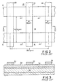
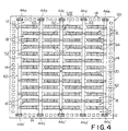
- the main power supply conductor strips 62 thus connecting the pairs of metal bumps 44 a to 44 e and 44 a ' to 44 e ' extend perpendicularly to the logic building blocks 16 and are bonded to local power distribution lines 64 implemented by thick-layer wiring strips forming a layer underlying the layer of the main power supply conductor strips 62.
- These local power distribution lines 64 are preferably formed concurrently with the formation of the metal bumps 44 a to 44 e and 44 a ' to 44 e ' on the semiconductor chip 60.
- the main power supply conductor strips 62 are thermocompression bonded to these local power distribution lines 64 and to the metal bumps 44 a to 44 e and 44 a ' to 44 e ' during the semiconductor wafer processing operation to fabricate the emitter-coupled logic gate array on the chip 60.
- Each of the logic building blocks 16 is composed of a row of three elementary cells 20 located between adjacent two of the main power supply conductor strips 64. It may be herein noted that there are no elementary cells 20 located below the main power supply conductor strips 62 so that the elementary cells 20 provided on the chip 60 are free from the mechanical stresses that will be created when the main power supply conductor strips 62 are bonded to the local power distribution lines 64 during wire bonding processing.
Landscapes
- Design And Manufacture Of Integrated Circuits (AREA)
- Semiconductor Integrated Circuits (AREA)
- Internal Circuitry In Semiconductor Integrated Circuit Devices (AREA)
Claims (2)
- Puce à semi-conducteur, comportant- un substrat,- une matrice de portes logiques comportant des blocs de construction logiques (16), constitués de cellules élémentaires (20), agencés en rangées parallèles sur le substrat entre deux zones (12) constituées de plages de connexion situées au niveau de bords opposés de la puce (60),- les rangées de blocs de construction logiques étant espacées les unes des autres pour former entre elles des canaux de connexion (18) parallèles,- des interconnexions (32) entre les cellules (20) s'étendant le long des canaux de connexion, une couche isolante (34) recouvrant lesdites interconnexions,- chacune desdites deux zones constituées de plages de connexion comportant des plages de connexion (14) avec des bosses métalliques (44i) espacées de manière à former avec les plages de l'autre zone une pluralité de paires de bosses métalliques opposées,- des bandes conductrices destinées à l'alimentation électrique principale (62) s'étendant entre les bosses de chaque paire de bosses métalliques et les reliant entre elles, les blocs de construction et les bandes conductrices destinées à l'alimentation électrique principale étant agencés de telle sorte qu'aucune cellule (20) ne soit située au-dessous desdites bandes,- les bandes conductrices destinées à l'alimentation électrique principale étant reliées à des lignes de distribution électriques (64), caractérisée en ce que- les lignes de distribution électriques (64) sont des bandes de connexion en couche épaisse formant une couche sous-jacente aux bandes conductrices destinées à l'alimentation électrique,- les bandes de connexion en couche épaisse sont identiques en termes de matériau et d'épaisseur aux bosses métalliques,- les bandes de connexion en couche épaisse sont branchées à partir des bandes conductrices destinées à l'alimentation électrique principale et s'étendent sur les blocs de construction logiques et le long de ceux-ci, mais pas les canaux de connexion (18), et- les bandes de connexion en couche épaisse sont formées sur ladite couche isolante, les bandes de connexion destinées à l'alimentation électrique enjambant les bandes de connexion en couche épaisse de telle sorte qu'une couche d'air soit présente entre chacune desdites bandes conductrices et la couche isolante.
- Procédé pour fabriquer une puce à semi-conducteur selon la revendication 1, caractérisé en ce qu'il comporte l'étape consistant à former les bandes de connexion en couche épaisse en concurrence avec les bosses métalliques et en utilisant le même matériau.
Applications Claiming Priority (2)
| Application Number | Priority Date | Filing Date | Title |
|---|---|---|---|
| JP63245053A JPH0290651A (ja) | 1988-09-28 | 1988-09-28 | 半導体集積回路 |
| JP245053/88 | 1988-09-28 |
Publications (3)
| Publication Number | Publication Date |
|---|---|
| EP0361825A2 EP0361825A2 (fr) | 1990-04-04 |
| EP0361825A3 EP0361825A3 (fr) | 1990-12-05 |
| EP0361825B1 true EP0361825B1 (fr) | 1997-07-23 |
Family
ID=17127880
Family Applications (1)
| Application Number | Title | Priority Date | Filing Date |
|---|---|---|---|
| EP89309719A Expired - Lifetime EP0361825B1 (fr) | 1988-09-28 | 1989-09-25 | Puce semi-conducteur et procédé de sa fabrication |
Country Status (4)
| Country | Link |
|---|---|
| US (1) | US5119168A (fr) |
| EP (1) | EP0361825B1 (fr) |
| JP (1) | JPH0290651A (fr) |
| DE (1) | DE68928193T2 (fr) |
Families Citing this family (18)
| Publication number | Priority date | Publication date | Assignee | Title |
|---|---|---|---|---|
| JP2965626B2 (ja) * | 1990-06-25 | 1999-10-18 | 株式会社東芝 | 半導体集積回路 |
| JP2677737B2 (ja) * | 1992-06-24 | 1997-11-17 | 株式会社東芝 | 半導体装置 |
| JP2930174B2 (ja) * | 1993-09-01 | 1999-08-03 | 日本電気株式会社 | 半導体集積回路装置 |
| JPH08106617A (ja) * | 1994-10-04 | 1996-04-23 | Fujitsu Ltd | 磁気ディスク装置 |
| US6098271A (en) * | 1994-10-04 | 2000-08-08 | Fujitsu Limited | Method for assembling a magnetic disk drive with a relaying flexible printed circuit sheet |
| US6049136A (en) * | 1998-06-03 | 2000-04-11 | Hewlett-Packard Company | Integrated circuit having unique lead configuration |
| JP4330676B2 (ja) * | 1998-08-17 | 2009-09-16 | 株式会社東芝 | 半導体集積回路 |
| JP4615117B2 (ja) * | 2000-11-21 | 2011-01-19 | パナソニック株式会社 | 半導体ウエハへのバンプ形成方法及びバンプ形成装置 |
| JP2002157582A (ja) * | 2000-11-21 | 2002-05-31 | Matsushita Electric Ind Co Ltd | 半導体ウエハ上のic傾き補正方法、及びic傾き補正装置 |
| US6653563B2 (en) | 2001-03-30 | 2003-11-25 | Intel Corporation | Alternate bump metallurgy bars for power and ground routing |
| US6888240B2 (en) | 2001-04-30 | 2005-05-03 | Intel Corporation | High performance, low cost microelectronic circuit package with interposer |
| US6894399B2 (en) | 2001-04-30 | 2005-05-17 | Intel Corporation | Microelectronic device having signal distribution functionality on an interfacial layer thereof |
| US7071024B2 (en) | 2001-05-21 | 2006-07-04 | Intel Corporation | Method for packaging a microelectronic device using on-die bond pad expansion |
| US7183658B2 (en) | 2001-09-05 | 2007-02-27 | Intel Corporation | Low cost microelectronic circuit package |
| US6825509B1 (en) * | 2001-11-26 | 2004-11-30 | Corrent Corporation | Power distribution system, method, and layout for an electronic device |
| US6538314B1 (en) * | 2002-03-29 | 2003-03-25 | International Business Machines Corporation | Power grid wiring for semiconductor devices having voltage islands |
| JP2010074018A (ja) * | 2008-09-22 | 2010-04-02 | Nec Electronics Corp | 半導体装置 |
| DE102013102542A1 (de) * | 2013-03-13 | 2014-09-18 | Schweizer Electronic Ag | Elektronisches Bauteil und Verfahren zum Herstellen eines elektronischen Bauteils |
Family Cites Families (5)
| Publication number | Priority date | Publication date | Assignee | Title |
|---|---|---|---|---|
| EP0060253A1 (fr) * | 1980-09-15 | 1982-09-22 | Mostek Corporation | Reseau de distribution de puissance a circuit integre |
| FR2495835A1 (fr) * | 1980-12-05 | 1982-06-11 | Cii Honeywell Bull | Dispositif a circuits integres a reseau metallique d'interconnexion, et procede de fabrication de ce dispositif |
| JPS5835963A (ja) * | 1981-08-28 | 1983-03-02 | Fujitsu Ltd | 集積回路装置 |
| IT1213261B (it) * | 1984-12-20 | 1989-12-14 | Sgs Thomson Microelectronics | Dispositivo a semiconduttore con metallizzazione a piu' spessori eprocedimento per la sua fabbricazione. |
| US4602270A (en) * | 1985-05-17 | 1986-07-22 | United Technologies Corporation | Gate array with reduced isolation |
-
1988
- 1988-09-28 JP JP63245053A patent/JPH0290651A/ja active Pending
-
1989
- 1989-09-25 EP EP89309719A patent/EP0361825B1/fr not_active Expired - Lifetime
- 1989-09-25 DE DE68928193T patent/DE68928193T2/de not_active Expired - Fee Related
- 1989-09-27 US US07/413,459 patent/US5119168A/en not_active Expired - Fee Related
Also Published As
| Publication number | Publication date |
|---|---|
| JPH0290651A (ja) | 1990-03-30 |
| DE68928193T2 (de) | 1997-11-13 |
| DE68928193D1 (de) | 1997-08-28 |
| US5119168A (en) | 1992-06-02 |
| EP0361825A3 (fr) | 1990-12-05 |
| EP0361825A2 (fr) | 1990-04-04 |
Similar Documents
| Publication | Publication Date | Title |
|---|---|---|
| EP0361825B1 (fr) | Puce semi-conducteur et procédé de sa fabrication | |
| EP0175870B1 (fr) | Dispositif à circuit intégré à l'échelle d'une plaquette semi-conductrice | |
| US6727597B2 (en) | Integrated circuit device having C4 and wire bond connections | |
| US5341049A (en) | Integrated circuit having alternate rows of logic cells and I/O cells | |
| US4412237A (en) | Semiconductor device | |
| EP0154998B1 (fr) | Structure de conducteurs d'alimentation dans un circuit intégré semi-conducteur | |
| JPH0587977B2 (fr) | ||
| CA1232364A (fr) | Ensemble integre a l'echelle des plaquettes | |
| KR910000155B1 (ko) | 반도체 집적회로장치 및 그 제조방법 | |
| US5093708A (en) | Multilayer integrated circuit module | |
| EP0517247A2 (fr) | Empaquetage multi-couche | |
| US6759329B2 (en) | Internal circuit structure of semiconductor chip with array-type bonding pads and method of fabricating the same | |
| EP0329018A2 (fr) | Circuit adapté à l'usager | |
| JP2580301B2 (ja) | 半導体集積回路装置 | |
| US20170154849A1 (en) | Semiconductor device comprising power elements in juxtaposition order | |
| CA1102009A (fr) | Schema de circuit integre a regions distinctes pour le cablage et pour les circuits actifs | |
| JPS6156440A (ja) | 回路基板結線構造 | |
| US4717988A (en) | Universal wafer scale assembly | |
| US7288846B2 (en) | Semiconductor chip having pads with plural junctions for different assembly methods | |
| US7466021B2 (en) | Memory packages having stair step interconnection layers | |
| EP0946980B1 (fr) | Structures de circuit integre ameliorees et procedes destines a faciliter la mesure precise des dispositifs d'un circuit integre | |
| JPH0576174B2 (fr) | ||
| EP0415106B1 (fr) | Des cadres conducteurs pour dispositif semi-conducteur | |
| US4857987A (en) | Semiconductor device | |
| JPS62183140A (ja) | 半導体集積回路装置 |
Legal Events
| Date | Code | Title | Description |
|---|---|---|---|
| PUAI | Public reference made under article 153(3) epc to a published international application that has entered the european phase |
Free format text: ORIGINAL CODE: 0009012 |
|
| 17P | Request for examination filed |
Effective date: 19891004 |
|
| AK | Designated contracting states |
Kind code of ref document: A2 Designated state(s): DE FR GB |
|
| PUAL | Search report despatched |
Free format text: ORIGINAL CODE: 0009013 |
|
| AK | Designated contracting states |
Kind code of ref document: A3 Designated state(s): DE FR GB |
|
| 17Q | First examination report despatched |
Effective date: 19931214 |
|
| GRAG | Despatch of communication of intention to grant |
Free format text: ORIGINAL CODE: EPIDOS AGRA |
|
| GRAH | Despatch of communication of intention to grant a patent |
Free format text: ORIGINAL CODE: EPIDOS IGRA |
|
| GRAH | Despatch of communication of intention to grant a patent |
Free format text: ORIGINAL CODE: EPIDOS IGRA |
|
| GRAA | (expected) grant |
Free format text: ORIGINAL CODE: 0009210 |
|
| AK | Designated contracting states |
Kind code of ref document: B1 Designated state(s): DE FR GB |
|
| REF | Corresponds to: |
Ref document number: 68928193 Country of ref document: DE Date of ref document: 19970828 |
|
| ET | Fr: translation filed | ||
| PLBE | No opposition filed within time limit |
Free format text: ORIGINAL CODE: 0009261 |
|
| STAA | Information on the status of an ep patent application or granted ep patent |
Free format text: STATUS: NO OPPOSITION FILED WITHIN TIME LIMIT |
|
| 26N | No opposition filed | ||
| PGFP | Annual fee paid to national office [announced via postgrant information from national office to epo] |
Ref country code: GB Payment date: 19980901 Year of fee payment: 10 |
|
| PGFP | Annual fee paid to national office [announced via postgrant information from national office to epo] |
Ref country code: FR Payment date: 19980922 Year of fee payment: 10 |
|
| PGFP | Annual fee paid to national office [announced via postgrant information from national office to epo] |
Ref country code: DE Payment date: 19981123 Year of fee payment: 10 |
|
| PG25 | Lapsed in a contracting state [announced via postgrant information from national office to epo] |
Ref country code: GB Free format text: LAPSE BECAUSE OF NON-PAYMENT OF DUE FEES Effective date: 19990925 |
|
| GBPC | Gb: european patent ceased through non-payment of renewal fee |
Effective date: 19990925 |
|
| PG25 | Lapsed in a contracting state [announced via postgrant information from national office to epo] |
Ref country code: FR Free format text: LAPSE BECAUSE OF NON-PAYMENT OF DUE FEES Effective date: 20000531 |
|
| PG25 | Lapsed in a contracting state [announced via postgrant information from national office to epo] |
Ref country code: DE Free format text: LAPSE BECAUSE OF NON-PAYMENT OF DUE FEES Effective date: 20000701 |
|
| REG | Reference to a national code |
Ref country code: FR Ref legal event code: ST |