EP0362867A2 - Procédé de fabrication de dispositifs semi-conducteurs - Google Patents
Procédé de fabrication de dispositifs semi-conducteurs Download PDFInfo
- Publication number
- EP0362867A2 EP0362867A2 EP89118588A EP89118588A EP0362867A2 EP 0362867 A2 EP0362867 A2 EP 0362867A2 EP 89118588 A EP89118588 A EP 89118588A EP 89118588 A EP89118588 A EP 89118588A EP 0362867 A2 EP0362867 A2 EP 0362867A2
- Authority
- EP
- European Patent Office
- Prior art keywords
- contact hole
- size
- forming
- insulation film
- defining area
- Prior art date
- Legal status (The legal status is an assumption and is not a legal conclusion. Google has not performed a legal analysis and makes no representation as to the accuracy of the status listed.)
- Granted
Links
Images



Classifications
-
- H—ELECTRICITY
- H10—SEMICONDUCTOR DEVICES; ELECTRIC SOLID-STATE DEVICES NOT OTHERWISE PROVIDED FOR
- H10W—GENERIC PACKAGES, INTERCONNECTIONS, CONNECTORS OR OTHER CONSTRUCTIONAL DETAILS OF DEVICES COVERED BY CLASS H10
- H10W20/00—Interconnections in chips, wafers or substrates
- H10W20/40—Interconnections external to wafers or substrates, e.g. back-end-of-line [BEOL] metallisations or vias connecting to gate electrodes
- H10W20/41—Interconnections external to wafers or substrates, e.g. back-end-of-line [BEOL] metallisations or vias connecting to gate electrodes characterised by their conductive parts
- H10W20/42—Vias, e.g. via plugs
-
- H—ELECTRICITY
- H10—SEMICONDUCTOR DEVICES; ELECTRIC SOLID-STATE DEVICES NOT OTHERWISE PROVIDED FOR
- H10W—GENERIC PACKAGES, INTERCONNECTIONS, CONNECTORS OR OTHER CONSTRUCTIONAL DETAILS OF DEVICES COVERED BY CLASS H10
- H10W20/00—Interconnections in chips, wafers or substrates
- H10W20/01—Manufacture or treatment
- H10W20/071—Manufacture or treatment of dielectric parts thereof
- H10W20/081—Manufacture or treatment of dielectric parts thereof by forming openings in the dielectric parts
-
- H—ELECTRICITY
- H10—SEMICONDUCTOR DEVICES; ELECTRIC SOLID-STATE DEVICES NOT OTHERWISE PROVIDED FOR
- H10P—GENERIC PROCESSES OR APPARATUS FOR THE MANUFACTURE OR TREATMENT OF DEVICES COVERED BY CLASS H10
- H10P50/00—Etching of wafers, substrates or parts of devices
- H10P50/73—Etching of wafers, substrates or parts of devices using masks for insulating materials
-
- H—ELECTRICITY
- H10—SEMICONDUCTOR DEVICES; ELECTRIC SOLID-STATE DEVICES NOT OTHERWISE PROVIDED FOR
- H10W—GENERIC PACKAGES, INTERCONNECTIONS, CONNECTORS OR OTHER CONSTRUCTIONAL DETAILS OF DEVICES COVERED BY CLASS H10
- H10W20/00—Interconnections in chips, wafers or substrates
- H10W20/01—Manufacture or treatment
- H10W20/071—Manufacture or treatment of dielectric parts thereof
- H10W20/092—Manufacture or treatment of dielectric parts thereof by smoothing the dielectric parts
-
- Y—GENERAL TAGGING OF NEW TECHNOLOGICAL DEVELOPMENTS; GENERAL TAGGING OF CROSS-SECTIONAL TECHNOLOGIES SPANNING OVER SEVERAL SECTIONS OF THE IPC; TECHNICAL SUBJECTS COVERED BY FORMER USPC CROSS-REFERENCE ART COLLECTIONS [XRACs] AND DIGESTS
- Y10—TECHNICAL SUBJECTS COVERED BY FORMER USPC
- Y10S—TECHNICAL SUBJECTS COVERED BY FORMER USPC CROSS-REFERENCE ART COLLECTIONS [XRACs] AND DIGESTS
- Y10S148/00—Metal treatment
- Y10S148/137—Resists
Definitions
- This invention relates to a method for manufacturing semiconductor devices, and more particularly to a method for manufacturing semiconductor devices having contact holes of different sizes via which the wirings thereof are made.
- a semiconductor integrated circuit is formed to have first and second wiring patterns which are laminated over a semiconductor substrate and are isolated from each other by means of an interlayer insulation film.
- the first wiring pattern is constituted by a plurality of lower wiring layers and the second wiring pattern is constituted by a plurality of upper wiring layers.
- the upper wiring layers are connected to the lower wiring layers via a plurality of contact holes formed in the interlayer insulation film.
- Each contact hole is formed in an area in which one set of upper and lower wiring layers connected to each other via the contact hole overlap each other.
- the sizes of the contact holes may vary depending on the withstand current determined for each contact hole.
- the matching margin A between the contact hole and the lower wiring layer and the matching margin B between the contact hole and the upper wiring layer are constant.
- the matching margin A is determined depending on an aligning error of a mask pattern used in a process for forming the first wiring pattern
- the matching margin B is determined depending on an aligning error of mask patterns used in processes for forming the contact hole and the first wiring pattern.
- the above semiconductor integrated circuit can be formed at relatively high yield when the integration density is low. However, if the width of the wiring is narrowed with an increase in the integration density and the size C of the contact hole is set, for example, to be less than 1.5 ⁇ m according to the width of the wiring, the manufacturing yield of the semiconductor integrated circuit is considerably lowered.
- An object of this invention is to provide a method for manufacturing semiconductor devices in which the manufacturing yield can be prevented form being lowered even when the contact hole is made small.
- the above object can be attained by a method for manufacturing semiconductor devices comprising the steps of forming a first wiring pattern including at least first and second lower conductive layers formed on a semiconductor substrate; forming an insulation film which covers the first wiring pattern; forming a first contact hole of a first size and a second contact hole of a second size larger than the first size in first and second areas of the insulation film which lie over the first and second lower conductive layers; forming a second wiring pattern having first and second upper conductive layers respectively connected to the first and second lower conductive layers via the first and second contact holes; wherein the contact hole formation step includes the sub-steps of forming a resist film which covers the insulation film; forming a resist pattern by effecting the photolithographic process of exposing the insulation film to light by using a mask pattern having a first contact hole defining area of a size substantially equal to the first size and a second contact hole defining area of a size smaller than the second size; and etching the insulation film with the resist pattern used as a mask; and the exposing
- the dependences of the resist pattern formation sub-step and the insulation film etching sub-step on the contact hole size can be cancelled.
- the size of the first contact hole is reduced to the first size which is less than 3 ⁇ m
- the first contact hole which is formed through the resist pattern formation sub-step and the insulation film etching sub-step may generally become smaller than the designed value, thereby increasing the contact resistance.
- the exposing light amount used in the resist pattern formation sub-step of the method of this invention is previously determined so that the size of the first contact hole which is formed in the insulation film etching sub-step may become equal to the first size or the designed value.
- the exposing light amount will increase in comparison with the normal case.
- the size of the second contact hole becomes larger than the second size and extends outwardly of an area on which the second lower conductive layer and the second upper conductive layer are overlapped.
- the reduced amount of the second hole defining area of the mask pattern is previously determined so that the size of the second contact hole which is formed in the insulation film etching sub-step can be set equal to the second size or the designed value. In this way, if the contact holes are formed with the designed sizes, reduction in the manufacturing yield due to miniaturization of the contact hole can be prevented. Further, since the miniaturization of the contact hole will not be limited by the dependency of the resist pattern formation sub-step and the insulation film etching sub-step on the contact hole size, the semiconductor device can be formed with a further increased integration density.
- Fig. 1 is a plan view of the semiconductor device and Fig. 2 is a cross sectional view of the semiconductor device taken along the line X-X of Fig. 1.
- the semiconductor device is a semiconductor integrated circuit having a number of semiconductor elements formed in the surface area of a semiconductor substrate 16. Two semiconductor elements 10A and 10B among the semiconductor elements are shown in Fig. 2. Wirings for the number of semiconductor elements are made by using first and second wiring patterns 11 and 12 which are disposed over the semiconductor substrate 16.
- the first and second wiring patterns 11 and 12 are formed of aluminum and are isolated from each other by means of interlayer insulation film 14 disposed between the first and second wiring patterns 11 and 12.
- the first wiring pattern 11 includes a plurality of wiring layers, for example, wiring layers 11A, 11B, 11C, which are formed on a silicon oxide film 15 covering the surface of the semiconductor substrate 16.
- the wiring layers 11A and 11C are connected to the semiconductor elements 10A and 10B via openings formed in the oxide film 15, thus serving as electrodes of the semiconductor elements 10A and 10B.
- the second wiring pattern 12 includes a plurality of wiring layers, for example, wiring layers 12A, 12B, 12C, which are formed on a silicon oxide film 15 covering the exposed surface of the oxide film 15 and the first wiring pattern 11 and serving as an interlayer insulation film 14.
- the wiring layers 12A, 12B and 12C are connected to the wiring layers 12A, 12B and 12C via contact holes 13A, 13B and 13C formed in the interlayer insulation film 14.
- the contact holes 13A, 13B and 13C are formed so as not to exceed outwardly of the areas of the interlayer insulation film 14 which lie over the wiring layers 12A, 12B and 12C.
- the reference positions of the contact holes are set at respective positions which are set behind the peripheries of the areas of the interlayer insulation film 14 by a preset distance corresponding to the matching margin A in the same manner as in the prior art.
- the width of the contact hole 13A is set at 3 ⁇ m and the width of the contact holes 13B and 13C is set at, for example, 1.5 ⁇ m which is less than 3 ⁇ m.
- the width of the contact hole is used to represent the size of the contact hole.
- a number of semiconductor elements for example, semiconductor elements 10A and 10B are formed in the surfaces area of the semiconductor substrate 16 and then the silicon oxide film 15 is formed to a thickness of 0.6 ⁇ m.
- the surfaces of the semiconductor substrate 16 and the semiconductor elements 10A and 10B are covered with the silicon oxide film 15. Openings are selectively formed in positions corresponding to the semiconductor elements 10A and 10B, for example, in the silicon oxide film 15 and then an aluminum layer is formed by deposition to a thickness of 1 ⁇ m on the exposed portions of the silicon oxide film 15 and the semiconductor elements 10A and 10B.
- the first wiring pattern 11 is formed by selectively removing the aluminum layer from the silicon layer 15 by using a mask pattern.
- the wiring layers 11A, 11B and 11C are formed of portions of the aluminum layer left behind on the silicon oxide film 15.
- a silicon oxide film 14A of a thickness of 1.1 ⁇ m is formed to cover the exposed portion of the first wiring pattern 11 and the silicon oxide film 15 by the plasma CVD method.
- the upper surface of the silicon oxide film 15 has convex and concave portions corresponding to the exposed portions of the first wiring pattern 11 and the silicon oxide film 15.
- a photoresist 17 is formed by coating on the silicon oxide film 14A so as to fill up the concave portions of the upper surface.
- the thickness of that portion of the photoresist 17 which lies on a portion other than the concave portion is set to 0.8 ⁇ m.
- the photoresist 17 is etched back by the thickness of 1.8 ⁇ m together with the convex portions of the silicon oxide film 14A. As a result, the upper surface of the silicon oxide film 14A is made flat.
- a silicon oxide film 14B is formed by deposition to a thickness of 1.4 ⁇ m on the silicon oxide film 14A by the plasma CVD method.
- the interlayer insulation film 14 is formed of the silicon oxide films 14A and 14B.
- a positive photoresist film 18 is uniformly formed by coating to a thickness of 1.5 ⁇ m on the upper surface of the interlayer oxide film 14 and is then subjected to a photolithographic process.
- a stepper is used to divide the plane of the photoresist film 18 into a plurality of areas and permit the areas to be sequentially exposed.
- a mask pattern as will be described later is used and the exposing light amount is set to an adequate value described later.
- the exposed portion of the photoresist film 18 is removed and the remaining portion of the photoresist film 18 is used to constitute a resist pattern 18A.
- RIE reactive ion etching
- an aluminum layer 12A is formed by deposition to a thickness of 1.0 ⁇ m on the exposed portion of the interlayer insulation film 14 and the first wiring pattern 11.
- the aluminum layer 12A is selectively removed from the interlayer insulation film 14 by using a mask pattern and the second wiring pattern 12 shown in Fig. 2 is formed of the remaining portion of the aluminum layer 12A.
- the photolithographic process effected in the step of Fig. 3E is explained in more detail.
- the contact hole defining area having the same size as the designed size of the contact hole is set in the mask pattern in the prior art.
- the exposing light amount is so determined that the size or width of the actually formed contact hole can be set to be equal to that of the contact hole defining area.
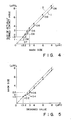
- the exposing light amount is determined so as to form a contact hole of 3 ⁇ m in the interlayer insulation film 14, this exposing light amount can be used for formation of a contact hole having a width of larger than 3 ⁇ m, for example, 4, 6 or 8 ⁇ m as shown by the line I in Fig. 4.
- the width of an actually formed contact hole is set to 1.6 ⁇ m.
- the width of an actually formed contact hole is set to 0.8 ⁇ m.
- the contact resistance between the two wiring layers connected to each other via the contact hole becomes extremely high.
- the exposing light amount is increased so as to set the width of the contact hole with 1.5 ⁇ m width to a designed value based on the above experiments, the width of an actually formed contact hole with more than 3 ⁇ m width is set to be larger than the designed value by 0.6 ⁇ m as shown by the line II of Fig. 4.
- the size of the defined area for the contact hole 13A is set to 2.4 ⁇ m which is smaller than the designed value by 0.6 ⁇ m and the size of the defined areas for the contact holes 13B and 13C is set to 1.5 ⁇ m which is equal to the designed value.
- the exposing light amount is set to be twice the stand and exposing light amount at which contact holes of not less than 3 ⁇ m width can be actually formed with the designed widths.
- Fig. 5 shows the size of the contact hole defining area of a mask pattern which is determined by the designed size of a contact hole
- Fig. 6 shows the relation between the increase in the exposing light amount and the increase in the contact hole size.
- contact holes of 1.5 and 3 ⁇ m widths can be formed with the designed values by changing the size of the mask pattern and at the same time effecting an excessive light exposing step in the photolithographic process.
- a contact hole of not larger than 1.5 ⁇ m width may be formed with the designed value, but a contact hole of not less than 1.5 ⁇ m width cannot be formed with the designed value and will be formed with a width larger than the designed value by 0.6 ⁇ m, which is set smaller than 0.7 ⁇ m due to the saturation shown in Fig. 6.
- the size of the contact hole defining area of a mask pattern used for formation of a contact hole with not less than 3 ⁇ m width is reduced by 0.6 ⁇ m in comparison with the designed value.
- Semiconductor integrated circuits having contact holes of various sizes ranging from 2 to 20 ⁇ m are manufactured as experiments according to the method of this embodiment.
- the mask aligning error of 0.3 ⁇ m and the etching error of 0.2 ⁇ m occur in the formation of these contact holes.
- the contact hole may not extend outwardly of the first wiring pattern. Since the matching margin A is used for the mask aligning error of 0.3 ⁇ m and the etching error of 0.2 ⁇ m, 0.2 ⁇ m is left unused in the matching margin A when the contact hole is formed with a designed size. Therefore, it was proved that a sufficiently high reliability could be obtained in the manufacturing process.
- the size of the contact hole will increased 0.6 ⁇ m.
- the size of the contact hole increases by 0.3 ⁇ m on one side thereof. Taking the mask aligning error of 0.3 ⁇ m and the etching error of 0.2 ⁇ m into consideration, there is a possibility that the contact hole may extend outwardly of the first wiring pattern when the matching margin A is set to 0.7 ⁇ m. In order to prevent this, it becomes necessary to set the matching margin A to at least 0.8 ⁇ m.
- the matching margin A it will be necessary to set the matching margin A to 1.0 ⁇ m. Assume that the semiconductor device is manufactured under a condition that the matching margin A is set to 1.0 ⁇ m and it includes 9,000 semiconductor elements. Then, the integration density of the semiconductor device manufactured according to the method of the above embodiment may be approx. 1.3 times that of the semiconductor device with the matching margin A of 1.0 ⁇ m.
- the exposing light amount is increased so that the contact holes 13B and 13C can be formed with designed sizes.
- the contact hole defining areas for the contact holes 13B and 13C are enlarged to prevent the contact holes 13B and 13C from being made smaller than the designed sizes.
- this method cannot reliably prevent the manufacturing yield from being lowered since the size of each of the contact holes 13B and 13C is remarkably changed if the size of the corresponding contact hole defining area is slightly changed due to a variation in the mask pattern formation process.
- the contact holes of 1.5 and 3 ⁇ m are provided to the semiconductor device.
- the size of the contact hole defining area of a mask pattern is set smaller than the designed size of this contact hole to prevent this contact hole from being made larger than the designed size, as is shown in Fig. 5.
- a contact hole smaller than 1.5 ⁇ m can be provided to the semiconductor device.
- the exposing light amount used in the step 3E is determined so that this contact hole is actually formed with the designed value.
- the exposing light amount is determined according to the size of the smallest one of the contact holes provided in the semiconductor device.
Landscapes
- Internal Circuitry In Semiconductor Integrated Circuit Devices (AREA)
- Drying Of Semiconductors (AREA)
- Exposure Of Semiconductors, Excluding Electron Or Ion Beam Exposure (AREA)
- Exposure And Positioning Against Photoresist Photosensitive Materials (AREA)
Applications Claiming Priority (2)
| Application Number | Priority Date | Filing Date | Title |
|---|---|---|---|
| JP63252701A JPH02100341A (ja) | 1988-10-06 | 1988-10-06 | 半導体装置のパターン形成方法 |
| JP252701/88 | 1988-10-06 |
Publications (3)
| Publication Number | Publication Date |
|---|---|
| EP0362867A2 true EP0362867A2 (fr) | 1990-04-11 |
| EP0362867A3 EP0362867A3 (fr) | 1992-07-08 |
| EP0362867B1 EP0362867B1 (fr) | 1994-04-13 |
Family
ID=17241049
Family Applications (1)
| Application Number | Title | Priority Date | Filing Date |
|---|---|---|---|
| EP89118588A Expired - Lifetime EP0362867B1 (fr) | 1988-10-06 | 1989-10-06 | Procédé de fabrication de dispositifs semi-conducteurs |
Country Status (5)
| Country | Link |
|---|---|
| US (1) | US4952528A (fr) |
| EP (1) | EP0362867B1 (fr) |
| JP (1) | JPH02100341A (fr) |
| KR (1) | KR930007840B1 (fr) |
| DE (1) | DE68914572T2 (fr) |
Cited By (1)
| Publication number | Priority date | Publication date | Assignee | Title |
|---|---|---|---|---|
| EP0426151A3 (en) * | 1989-10-31 | 1993-08-11 | Kabushiki Kaisha Toshiba | Multi-layered wiring structure of semiconductor integrated circuit device |
Families Citing this family (15)
| Publication number | Priority date | Publication date | Assignee | Title |
|---|---|---|---|---|
| US5849632A (en) * | 1991-08-30 | 1998-12-15 | Micron Technology, Inc. | Method of passivating semiconductor wafers |
| JP2727909B2 (ja) * | 1993-03-26 | 1998-03-18 | 松下電器産業株式会社 | 金属配線の形成方法 |
| US5286675A (en) * | 1993-04-14 | 1994-02-15 | Industrial Technology Research Institute | Blanket tungsten etchback process using disposable spin-on-glass |
| JP2947054B2 (ja) * | 1994-03-04 | 1999-09-13 | ヤマハ株式会社 | 配線形成法 |
| US5464794A (en) * | 1994-05-11 | 1995-11-07 | United Microelectronics Corporation | Method of forming contact openings having concavo-concave shape |
| US5646814A (en) | 1994-07-15 | 1997-07-08 | Applied Materials, Inc. | Multi-electrode electrostatic chuck |
| US5592358A (en) | 1994-07-18 | 1997-01-07 | Applied Materials, Inc. | Electrostatic chuck for magnetic flux processing |
| US5846876A (en) * | 1996-06-05 | 1998-12-08 | Advanced Micro Devices, Inc. | Integrated circuit which uses a damascene process for producing staggered interconnect lines |
| US5866481A (en) * | 1996-06-07 | 1999-02-02 | Taiwan Semiconductor Manufacturing Company Ltd. | Selective partial curing of spin-on-glass by ultraviolet radiation to protect integrated circuit dice near the wafer edge |
| US6255039B1 (en) * | 1997-04-16 | 2001-07-03 | Isola Laminate Systems Corp. | Fabrication of high density multilayer interconnect printed circuit boards |
| JP2001308002A (ja) * | 2000-02-15 | 2001-11-02 | Canon Inc | フォトマスクを用いたパターン作製方法、及びパターン作製装置 |
| US7136681B2 (en) * | 2001-10-31 | 2006-11-14 | Telefonaktiebolaget Lm Ericsson (Publ) | Electrically conductive carrier and patterning for controlling current distribution in a wireless communications device |
| US7404167B2 (en) * | 2005-02-23 | 2008-07-22 | Taiwan Semiconductor Manufacturing Company, Ltd. | Method for improving design window |
| JP4665631B2 (ja) * | 2005-07-07 | 2011-04-06 | セイコーエプソン株式会社 | 電子基板とその製造方法及び電気光学装置の製造方法並びに電子機器の製造方法 |
| KR102678267B1 (ko) * | 2016-10-12 | 2024-06-25 | 주성엔지니어링(주) | 기판처리장치 및 기판처리방법 |
Family Cites Families (2)
| Publication number | Priority date | Publication date | Assignee | Title |
|---|---|---|---|---|
| US4253888A (en) * | 1978-06-16 | 1981-03-03 | Matsushita Electric Industrial Co., Ltd. | Pretreatment of photoresist masking layers resulting in higher temperature device processing |
| NL181611C (nl) * | 1978-11-14 | 1987-09-16 | Philips Nv | Werkwijze ter vervaardiging van een bedradingssysteem, alsmede een halfgeleiderinrichting voorzien van een dergelijk bedradingssysteem. |
-
1988
- 1988-10-06 JP JP63252701A patent/JPH02100341A/ja active Granted
-
1989
- 1989-10-04 US US07/416,779 patent/US4952528A/en not_active Expired - Lifetime
- 1989-10-06 EP EP89118588A patent/EP0362867B1/fr not_active Expired - Lifetime
- 1989-10-06 DE DE68914572T patent/DE68914572T2/de not_active Expired - Fee Related
- 1989-10-06 KR KR1019890014372A patent/KR930007840B1/ko not_active Expired - Fee Related
Cited By (1)
| Publication number | Priority date | Publication date | Assignee | Title |
|---|---|---|---|---|
| EP0426151A3 (en) * | 1989-10-31 | 1993-08-11 | Kabushiki Kaisha Toshiba | Multi-layered wiring structure of semiconductor integrated circuit device |
Also Published As
| Publication number | Publication date |
|---|---|
| DE68914572D1 (de) | 1994-05-19 |
| JPH0587179B2 (fr) | 1993-12-15 |
| JPH02100341A (ja) | 1990-04-12 |
| KR900007050A (ko) | 1990-05-09 |
| DE68914572T2 (de) | 1994-09-01 |
| KR930007840B1 (ko) | 1993-08-20 |
| US4952528A (en) | 1990-08-28 |
| EP0362867A3 (fr) | 1992-07-08 |
| EP0362867B1 (fr) | 1994-04-13 |
Similar Documents
| Publication | Publication Date | Title |
|---|---|---|
| EP0362867A2 (fr) | Procédé de fabrication de dispositifs semi-conducteurs | |
| EP0766303B1 (fr) | Dispositif semi-conducteur ayant une gorge de connexion et un trou de contact formés de façon auto-alignée et son procédé de fabrication | |
| EP0239489B1 (fr) | Procédé pour former des trous de liaison sur un circuit intégré | |
| US4070501A (en) | Forming self-aligned via holes in thin film interconnection systems | |
| US5618757A (en) | Method for improving the manufacturability of the spin-on glass etchback process | |
| KR920004541B1 (ko) | 반도체 소자에서 식각베리어층을 사용한 콘택홀 형성방법 | |
| US6133635A (en) | Process for making self-aligned conductive via structures | |
| JPH0691033B2 (ja) | 半導体構造上の接点スタッドの製造方法 | |
| KR950011555B1 (ko) | 반도체 접속장치 및 그 제조방법 | |
| US6326278B1 (en) | Method of protecting an alignment mark when manufacturing a semiconductor device | |
| US6614643B1 (en) | Semiconductor device having a capacitor element | |
| CA1120611A (fr) | Faconnage des raccordements pour circuits imprimes pluri-etages | |
| US20030062592A1 (en) | Fuse element, semiconductor device and method for manufacturing the same | |
| KR19980014210A (ko) | 반도체 장치 및 그 제조방법 | |
| TWI248144B (en) | Semiconductor element having alignment post electrode and method of manufacturing the same | |
| US5877082A (en) | Method of manufacturing semiconductor device without plasma damage | |
| KR19980020482A (ko) | 반도체 장치의 배선구조 및 방법 | |
| US6169664B1 (en) | Selective performance enhancements for interconnect conducting paths | |
| US6287902B1 (en) | Methods of forming etch inhibiting structures on field isolation regions | |
| KR100265991B1 (ko) | 반도체 장치의 다층 배선간 연결공정 | |
| US5338397A (en) | Method of forming a semiconductor device | |
| KR100372102B1 (ko) | 반도체 소자의 스티칭 공정방법 | |
| KR0140483B1 (ko) | 반도체소자의 금속배선 제조방법 | |
| KR100340858B1 (ko) | 반도체 소자의 금속배선 형성방법 | |
| KR950003224B1 (ko) | 다층배선 구조를 갖는 반도체 장치의 제조방법 |
Legal Events
| Date | Code | Title | Description |
|---|---|---|---|
| PUAI | Public reference made under article 153(3) epc to a published international application that has entered the european phase |
Free format text: ORIGINAL CODE: 0009012 |
|
| 17P | Request for examination filed |
Effective date: 19891006 |
|
| AK | Designated contracting states |
Kind code of ref document: A2 Designated state(s): DE FR GB |
|
| PUAL | Search report despatched |
Free format text: ORIGINAL CODE: 0009013 |
|
| AK | Designated contracting states |
Kind code of ref document: A3 Designated state(s): DE FR GB |
|
| 17Q | First examination report despatched |
Effective date: 19930107 |
|
| GRAA | (expected) grant |
Free format text: ORIGINAL CODE: 0009210 |
|
| AK | Designated contracting states |
Kind code of ref document: B1 Designated state(s): DE FR GB |
|
| REF | Corresponds to: |
Ref document number: 68914572 Country of ref document: DE Date of ref document: 19940519 |
|
| ET | Fr: translation filed | ||
| PLBE | No opposition filed within time limit |
Free format text: ORIGINAL CODE: 0009261 |
|
| STAA | Information on the status of an ep patent application or granted ep patent |
Free format text: STATUS: NO OPPOSITION FILED WITHIN TIME LIMIT |
|
| 26N | No opposition filed | ||
| PGFP | Annual fee paid to national office [announced via postgrant information from national office to epo] |
Ref country code: FR Payment date: 19971009 Year of fee payment: 9 |
|
| PGFP | Annual fee paid to national office [announced via postgrant information from national office to epo] |
Ref country code: DE Payment date: 19971010 Year of fee payment: 9 |
|
| REG | Reference to a national code |
Ref country code: GB Ref legal event code: 746 Effective date: 19980909 |
|
| PG25 | Lapsed in a contracting state [announced via postgrant information from national office to epo] |
Ref country code: FR Free format text: LAPSE BECAUSE OF NON-PAYMENT OF DUE FEES Effective date: 19990630 |
|
| REG | Reference to a national code |
Ref country code: FR Ref legal event code: ST |
|
| PG25 | Lapsed in a contracting state [announced via postgrant information from national office to epo] |
Ref country code: DE Free format text: LAPSE BECAUSE OF NON-PAYMENT OF DUE FEES Effective date: 19990803 |
|
| REG | Reference to a national code |
Ref country code: GB Ref legal event code: IF02 |
|
| PGFP | Annual fee paid to national office [announced via postgrant information from national office to epo] |
Ref country code: GB Payment date: 20071003 Year of fee payment: 19 |
|
| GBPC | Gb: european patent ceased through non-payment of renewal fee |
Effective date: 20081006 |
|
| PG25 | Lapsed in a contracting state [announced via postgrant information from national office to epo] |
Ref country code: GB Free format text: LAPSE BECAUSE OF NON-PAYMENT OF DUE FEES Effective date: 20081006 |