EP0363076B1 - Vielfachhalbleiterlaser mit grosser Ausgangsleistung und hoher Strahlqualität - Google Patents
Vielfachhalbleiterlaser mit grosser Ausgangsleistung und hoher Strahlqualität Download PDFInfo
- Publication number
- EP0363076B1 EP0363076B1 EP89309891A EP89309891A EP0363076B1 EP 0363076 B1 EP0363076 B1 EP 0363076B1 EP 89309891 A EP89309891 A EP 89309891A EP 89309891 A EP89309891 A EP 89309891A EP 0363076 B1 EP0363076 B1 EP 0363076B1
- Authority
- EP
- European Patent Office
- Prior art keywords
- waveguides
- array
- semiconductor laser
- mode
- laser array
- Prior art date
- Legal status (The legal status is an assumption and is not a legal conclusion. Google has not performed a legal analysis and makes no representation as to the accuracy of the status listed.)
- Expired - Lifetime
Links
- 239000004065 semiconductor Substances 0.000 title claims description 40
- LFEUVBZXUFMACD-UHFFFAOYSA-H lead(2+);trioxido(oxo)-$l^{5}-arsane Chemical compound [Pb+2].[Pb+2].[Pb+2].[O-][As]([O-])([O-])=O.[O-][As]([O-])([O-])=O LFEUVBZXUFMACD-UHFFFAOYSA-H 0.000 claims description 24
- 230000005855 radiation Effects 0.000 claims description 23
- 239000000758 substrate Substances 0.000 claims description 14
- 238000005253 cladding Methods 0.000 claims description 9
- 230000009471 action Effects 0.000 claims description 7
- 239000000463 material Substances 0.000 claims description 6
- 230000000737 periodic effect Effects 0.000 claims description 4
- 239000012071 phase Substances 0.000 description 52
- 238000003491 array Methods 0.000 description 31
- 230000008878 coupling Effects 0.000 description 16
- 238000010168 coupling process Methods 0.000 description 16
- 238000005859 coupling reaction Methods 0.000 description 16
- 230000000694 effects Effects 0.000 description 11
- 230000008901 benefit Effects 0.000 description 8
- 238000009826 distribution Methods 0.000 description 7
- 238000000034 method Methods 0.000 description 7
- FTWRSWRBSVXQPI-UHFFFAOYSA-N alumanylidynearsane;gallanylidynearsane Chemical compound [As]#[Al].[As]#[Ga] FTWRSWRBSVXQPI-UHFFFAOYSA-N 0.000 description 5
- JBRZTFJDHDCESZ-UHFFFAOYSA-N AsGa Chemical compound [As]#[Ga] JBRZTFJDHDCESZ-UHFFFAOYSA-N 0.000 description 4
- 230000003287 optical effect Effects 0.000 description 4
- 239000007787 solid Substances 0.000 description 4
- 229910001218 Gallium arsenide Inorganic materials 0.000 description 3
- 238000010521 absorption reaction Methods 0.000 description 3
- 229910052782 aluminium Inorganic materials 0.000 description 3
- XAGFODPZIPBFFR-UHFFFAOYSA-N aluminium Chemical compound [Al] XAGFODPZIPBFFR-UHFFFAOYSA-N 0.000 description 3
- 238000013459 approach Methods 0.000 description 3
- 238000001914 filtration Methods 0.000 description 3
- 238000005229 chemical vapour deposition Methods 0.000 description 2
- 230000001066 destructive effect Effects 0.000 description 2
- 230000014509 gene expression Effects 0.000 description 2
- 238000003384 imaging method Methods 0.000 description 2
- 230000006872 improvement Effects 0.000 description 2
- 238000004943 liquid phase epitaxy Methods 0.000 description 2
- 238000005457 optimization Methods 0.000 description 2
- 230000010363 phase shift Effects 0.000 description 2
- 229910000530 Gallium indium arsenide Inorganic materials 0.000 description 1
- KXNLCSXBJCPWGL-UHFFFAOYSA-N [Ga].[As].[In] Chemical compound [Ga].[As].[In] KXNLCSXBJCPWGL-UHFFFAOYSA-N 0.000 description 1
- 239000011149 active material Substances 0.000 description 1
- 230000015556 catabolic process Effects 0.000 description 1
- 230000008859 change Effects 0.000 description 1
- 239000013078 crystal Substances 0.000 description 1
- 238000006731 degradation reaction Methods 0.000 description 1
- 230000001419 dependent effect Effects 0.000 description 1
- 238000013461 design Methods 0.000 description 1
- 230000005284 excitation Effects 0.000 description 1
- 239000012535 impurity Substances 0.000 description 1
- 238000002347 injection Methods 0.000 description 1
- 239000007924 injection Substances 0.000 description 1
- 238000007689 inspection Methods 0.000 description 1
- 238000004519 manufacturing process Methods 0.000 description 1
- 229910052751 metal Inorganic materials 0.000 description 1
- 239000002184 metal Substances 0.000 description 1
- 238000012986 modification Methods 0.000 description 1
- 230000004048 modification Effects 0.000 description 1
- 238000001451 molecular beam epitaxy Methods 0.000 description 1
- 230000010355 oscillation Effects 0.000 description 1
- 230000008569 process Effects 0.000 description 1
- 230000001902 propagating effect Effects 0.000 description 1
- 238000011160 research Methods 0.000 description 1
Images


Classifications
-
- H—ELECTRICITY
- H01—ELECTRIC ELEMENTS
- H01S—DEVICES USING THE PROCESS OF LIGHT AMPLIFICATION BY STIMULATED EMISSION OF RADIATION [LASER] TO AMPLIFY OR GENERATE LIGHT; DEVICES USING STIMULATED EMISSION OF ELECTROMAGNETIC RADIATION IN WAVE RANGES OTHER THAN OPTICAL
- H01S5/00—Semiconductor lasers
- H01S5/40—Arrangement of two or more semiconductor lasers, not provided for in groups H01S5/02 - H01S5/30
- H01S5/4025—Array arrangements, e.g. constituted by discrete laser diodes or laser bar
- H01S5/4031—Edge-emitting structures
- H01S5/4062—Edge-emitting structures with an external cavity or using internal filters, e.g. Talbot filters
-
- H—ELECTRICITY
- H01—ELECTRIC ELEMENTS
- H01S—DEVICES USING THE PROCESS OF LIGHT AMPLIFICATION BY STIMULATED EMISSION OF RADIATION [LASER] TO AMPLIFY OR GENERATE LIGHT; DEVICES USING STIMULATED EMISSION OF ELECTROMAGNETIC RADIATION IN WAVE RANGES OTHER THAN OPTICAL
- H01S5/00—Semiconductor lasers
- H01S5/10—Construction or shape of the optical resonator, e.g. extended or external cavity, coupled cavities, bent-guide, varying width, thickness or composition of the active region
- H01S5/14—External cavity lasers
- H01S5/148—External cavity lasers using a Talbot cavity
-
- H—ELECTRICITY
- H01—ELECTRIC ELEMENTS
- H01S—DEVICES USING THE PROCESS OF LIGHT AMPLIFICATION BY STIMULATED EMISSION OF RADIATION [LASER] TO AMPLIFY OR GENERATE LIGHT; DEVICES USING STIMULATED EMISSION OF ELECTROMAGNETIC RADIATION IN WAVE RANGES OTHER THAN OPTICAL
- H01S5/00—Semiconductor lasers
- H01S5/40—Arrangement of two or more semiconductor lasers, not provided for in groups H01S5/02 - H01S5/30
- H01S5/4025—Array arrangements, e.g. constituted by discrete laser diodes or laser bar
- H01S5/4031—Edge-emitting structures
- H01S5/4068—Edge-emitting structures with lateral coupling by axially offset or by merging waveguides, e.g. Y-couplers
Definitions
- This invention relates generally to semiconductor diode lasers and, more particularly, to one-dimensional arrays of semiconductor diode lasers fabricated as monolithic structures.
- Single-element diode lasers are limited in power to outputs of the order of 30 milliwatts (mW), but arrays of diode lasers can be designed to provide output powers of hundreds of milliwatts. Such high power outputs are useful in optical communications systems, laser printers and other applications.
- phase-locked laser arrays A survey of the state of the art of phase-locked laser arrays can be found in a paper entitled “Phase-Locked Arrays of Semiconductor Diode Lasers,” by Dan Botez and Donald Ackley, IEEE Circuits and Devices Magazine, Vol. 2, No. 1, pp. 8-17, January 1986.
- a semiconductor diode laser is a multilayered structure composed of different types of semiconductor materials, chemically doped with impurities to give them either an excess of electrons (n type) or an excess of electron vacancies or holes (p type).
- the basic structure of the semiconductor laser is that of a diode, having an n type layer, a p type layer, and an undoped active layer sandwiched between them. When the diode is forward-biased in normal operation, electrons and holes recombine in the region of the active layer, and light is emitted.
- the layers on each side of the active layer usually have a lower index of refraction than the active layer, and function as cladding layers in a dielectric waveguide that confines the light in a direction perpendicular to the layers.
- Various techniques are usually employed to confine the light in a lateral direction as well, and crystal facets are located at opposite ends of the structure, to provide for repeated reflections of the light back and forth in a longitudinal direction in the structure. If the diode current is above a threshold value, lasing takes place and light is emitted from one of the facets, in a direction generally perpendicular to the emitting facet.
- an array of laser emitters can oscillate in one or more of multiple possible configurations, known as array modes.
- array modes In what is usually considered to be the most desirable array mode, all of the emitters oscillate in phase. This is known as the fundamental or 0°-phase-shift array mode, and it produces a far-field pattern in which most of the energy is concentrated in a single lobe, the width of which is limited, ideally, only by the diffraction of light.
- the array operates in the 180°-phase-shift array mode, or out-of-phase array mode, and produces two relatively widely spaced lobes in the far-field distribution pattern.
- N-element arrays Multiple additional modes exist between these two extremes, depending on the phase alignment of the separate emitters, and in general there are N possible array modes for an N-element array.
- Many laser arrays operate in two or three array modes simultaneously and produce one or more beams that are typically two or three times wider than the diffraction limit.
- United States Patent US-A-4,723,252 discloses a phase-locked laser array comprising a substrate with two spaced-apart pluralities of channels extending towards different reflecting surfaces of the array.
- the axes of symmetry of the channels of one plurality are offset from the axes of symmetry of the other plurality. Coupling of light propagating in the optical waveguides over one plurality of channels into the waveguides over the other plurality of channels is said to induce zero phase difference between the laser oscillations of adjacent channels.
- Preferred embodiments of the present invention address two closely related problems pertaining to the operation of laser arrays at high powers and with high beam quality.
- the first problem involves the continuing search for a laser array structure of higher brightness (power per unit angle), operating in a selected array mode and without sacrificing efficiency and compactness.
- Some embodiments of the present invention address this need and provide a high-power output laser array operating in either the fundamental (in-phase) array mode or the out-of-phase array mode.
- the second major problem area is the subject of European application 91109377.1, a divisional of the present application, and pertains to the degree of coherence and uniformity of output intensities that can be obtained across a laser array.
- Prior to that invention coupling between lasers was limited to "nearest-neighbor" coupling to only adjacent lasers. This provided only a limited degree of overall coherence, and a characteristic cosine-shaped near-field intensity distribution.
- preferred embodiments of the present invention aim to provide a semiconductor laser array with a high degree of device coherence and a practically uniform near-field intensity distribution from a laser array.
- a semiconductor laser array structure comprising:
- the diffraction region has a length equal to an odd multiple of half the Talbot length and the two arrays of waveguides are selectively aligned with each other in a lateral sense, and operate as a spatial filter to eliminate unwanted array modes from the output of the structure.
- the two arrays are offset from each other laterally by one half of the periodic element spacing, such that the active laser elements of one array are aligned with interelement regions of the other array. This configuration favors operation in the fundamental array mode and effectively eliminates the out-of-phase mode from the device output.
- the active lasing elements of each array are in approximate alignment and this favors operation in the out-of-phase array mode only.
- the diffraction region length may also be made an even multiple of half Talbot lengths, such as one full Talbot length, with the device further including means for suppressing the out-of-phase array mode.
- the structure as described thus far could employ two separately fabricated arrays separated by the laterally unguided diffraction region.
- the entire structure is monolithic. That is to say, the diffraction region is a semiconductor structure integrated with the semiconductor arrays.
- the diffraction region may be an active semiconductor laser region, using such a separate electrode, or a common electrode with the arrays of waveguides, or the diffraction region may be a passive planar waveguide, with no electrodes.
- the preferred form of the invention uses antiguides for the two arrays of waveguides, although positive-index waveguides could alternatively be employed. Another preference is to use one half of the first Talbot distance for the length of the diffraction region. Multiples of this length should also produce the same results.
- a practically uniform near-field intensity distribution is obtained from a laser array by utilizing a resonance condition that occurs in an array of antiguides structured to fall within or near a narrow range of parameters that favor the condition. More specifically, for a given operating wavelength, the width, interelement spacing, and refractive indices of the antiguides are selected to produce an operating point at or close to the resonance condition, in which there is coupling not just between adjacent waveguides, but between all of the waveguides, i.e. coupling from each waveguide element to all other elements in the array. With this complete or parallel coupling, device coherence is maximized and a practically uniform near-field distribution is obtained.
- a semiconductor laser array in accordance with such embodiments of the invention comprises means for producing lasing action in the structure, and a set of negative-index waveguides with parallel longitudinal axes, having a lateral antiguide elemental width of d0 and an interelement spacing s.
- the waveguides generate laterally traveling waves that have a wavelength ⁇ 0, equal to approximately 2d0, in the antiguide elements and a wavelength ⁇ 1 in the interelement regions.
- the interelement spacing s is selected to be approximately equal to an odd number of half-wavelengths, or m ⁇ 1/2, where m is an odd integer, to produce a fundamental-array-mode resonance condition in which there is strong coupling between all elements of the array and a high degree of device coherence.
- the device also includes means within the array structure for suppressing operation in the out-of-phase array mode.
- the wavelength ⁇ 1 of laterally traveling waves in the interelement regions is dependent on the difference An between the (transverse) effective refractive index of the antiguide element and the (transverse) effective refractive index of the interelement region.
- this index difference and the spacing s are selected to provide an operating point close enough to the resonance condition to give strong coupling between all elements of the array, but to provide in addition strong discrimination between the fundamental mode and adjacent higher-order modes.
- One approach to providing means for suppressing the out-of-phase mode in this structure is to include an interelement semiconductor structure for introducing interelement losses, which inhibit operation in the out-of-phase array mode.
- This may take the form of a transverse antiguiding structure that permits significant radiation loss to the substrate, or may include an absorbing layer providing absorption loss in the interelement regions.
- an important embodiment of the invention is one in which the Talbot effect is utilized in conjunction with a spatial filter to eliminate undesirable array modes, and the arrays of the device are constructed as antiguides conforming to or closely approaching the defined resonance condition.
- the present invention represents a significant advance in the field of semiconductor laser arrays.
- the invention permits operation at relatively high powers and drive currents without degradation of beam quality and in a selected mode, with high efficiency and device coherence.
- the present invention is concerned with improvements in the field of semiconductor laser arrays.
- the invention relates to the operation of a laser array at high power levels by utilizing the Talbot effect in combination with some means internal to the array structure, for suppressing out-of-phase array mode operation.
- a preferred embodiment of the invention additionally relates to the improvement of operating characteristics provided when an array of antiguides is operated at a selected condition at or near a resonance point.
- the Talbot effect is a diffraction phenomenon first observed in the nineteenth century.
- the diffracted light recombines into images of the emitters at a plane located at a predictable distance from the array, known as one Talbot length.
- the first Talbot length is given by 2d/ ⁇ , where d is the periodic spacing of the light emitters and ⁇ is the wavelength of the emitted light in the diffraction medium.
- re-imaging takes place at other additional points spaced further from the emitters, and given by the expression 2nd/ ⁇ , where n is an integer.
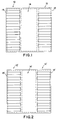
- FIG. 1 The embodiment of the invention shown in FIG. 1 includes a first array of semiconductor laser waveguides, indicated generally by reference numeral 10, and a second array of semiconductor laser waveguides 12.
- Each array has laser elements that are periodically spaced by a distance d0, and the arrays are separated by a laterally unguided region 14 having a width approximately equal to one-half of the Talbot distance.
- the elements of the array 10 are aligned with the interelement regions array 12, and this favors operation in the fundamental or in-phase array mode.
- the arrays 10 and 12 are cleaved at their ends remote from the diffraction region 14, to provide mirrored surfaces 15, and, as will be discussed, the cross-sections of the arrays are conventionally fabricated to provide either positive- or negative-index guiding of light.
- emissions from this array will be transmitted through the diffraction region 14, and re-imaged at the midpoints of regions between the original emitting laser elements, i.e. at the centers of the waveguides in the other laser array.
- Emissions in the out-of-phase mode will be re-imaged at the same laterally spaced locations as the emitting array, i.e. at the midpoints of interelement regions in the opposite array, and will be effectively suppressed by a spatial filtering effect provided by the selected lateral positions of the two arrays.
- the device of FIG. 2 is identical with that of FIG. 1 except for the lateral alignment of the two arrays, referred to as 10' and 12' in FIG. 2.
- the two arrays are at least approximately aligned, and out-of-phase array mode emissions from one array are launched directly into the other array, since the out-of-phase radiation is re-imaged in its original form at one-half the Talbot distance.
- the in-phase mode is suppressed because of its being re-imaged in interelement regions in the FIG. 2 version of the invention.
- 180-degree phase shifters may be employed external to or on the device, at positions corresponding to alternate elements. Alternatively, there may be some applications in which the out-of-phase mode is desirable.
- the diffraction region 14 is, in general, any integral multiple of one-half of the Talbot distance. That is, the length of the region may be expressed generally as (2n-1)d 0 2 / ⁇ , where n is a positive integer.
- FIG. 2 may also be considered to illustrate another variant form of the invention, in which the length of the diffraction region 14' is an even multiple of half of the Talbot distance, for example one full Talbot distance.
- both the fundamental and the out-of-phase array modes are re-imaged and some additional means must be provided, internal to the structure of the device, to suppress the out-of-phase mode.
- This means may take various forms, some of which are described later in this specification.
- the particular structure of the waveguides 10 and 12 is not critical to the invention in its broadest sense.
- the waveguides may employ positive index guiding or negative index guiding.
- One presently preferred embodiment of the invention takes the form of arrays of antiguides, as shown by way of example in FIG. 3.
- the semiconductor array structure includes a substrate 16 of p+ type gallium arsenide (GaAs) on which is formed a layer 17 of p type aluminum gallium arsenide having 30% aluminum (Al 0.3 Ga 0.7 As) and a buffer layer 18 of n or p type aluminum gallium arsenide having 10% aluminum (Al 0.1 Ga 0.9 As).
- the lasing element is defined in part by channels 20 formed through the layers 17 and 18, and part-way into the substrate 16.
- An active layer 24 of undoped GaAs is formed over the first cladding layer 22, and a second cladding layer 26 of n type Al 0.3 Ga 0.7 As is formed over the active layer.
- the active layer 24 is undoped and the cladding layers 22 and 26 are appropriately doped to provide a diode action across the active layer as a p-n junction.
- the structure is capped with another layer of n+ type gallium arsenide and a metal layer for electrical contact, neither of which is shown.
- an additional contact layer is formed on the undersurface of the substrate 16.
- the effective index of refraction is lower in the regions of the channels 20 than in the interelement regions between channels. Therefore the channels 20 form an array of antiguides in a lateral sense. As disclosed in United States Patent US 4,860,298, such an array provides both strong mode confinement and strong interelement coupling.
- the arrays 10 and 12 employ lateral antiguiding, although positive index guiding may be employed as an alternative.
- the semiconductor materials are either aluminum gallium arsenide (AlGaAs) or indium gallium arsenide phosphide (InGaAsP), depending on the desired wavelength, but other semiconductor laser materials may be used.
- AlGaAs aluminum gallium arsenide
- InGaAsP indium gallium arsenide phosphide
- the active material type includes quantum well, separately confined heterostructures, but again this is not critical to the invention.
- the fabrication method presently contemplated is metal-organic chemical vapor deposition (MOCVD), but liquid phase epitaxy (LPE), molecular beam epitaxy (MBE) and other chemical vapor deposition techniques may also be employed.
- a principal advantage of the invention is that it provides increased power per unit solid angle, compared with similar structures not employing the diffraction region and the spatial filtering approach.
- arrays using these principles may be scaled up in width without decrease of power per unit solid angle.
- Another advantage is that the guided and unguided regions of the structure may be separately controlled by separate current electrodes, thereby permitting optimization of device performance by optimizing each region separately.
- One alternative is to design the diffraction region as a passive planar waveguide, with no electrodes.
- Still another advantage of the device is its improved discrimination against unwanted array modes.
- a preferred embodiment of the invention relates to the use of a resonant or nearly resonant condition in an array of antiguides, to achieve fundamental array mode operation at the highest possible power levels.
- interelement coupling in linear arrays of semiconductor laser waveguides is limited to coupling between adjacent waveguides.
- This neighbor-to-neighbor coupling produces a characteristic cosine-shaped near-field intensity distribution pattern, and gives poor overall coherence across the device.
- all of the array elements should be equally coupled to each other, and for maximum efficiency the near-field intensity profile should be as near uniform as possible.
- Another requirement for maximum single-mode power is that the discrimination between the fundamental mode and the nearest higher-order mode should be maximized.
- FIG. 6 shows a central antiguide core region of width d0 and (transverse) effective refractive index n 0, surrounded by two cladding regions of higher (transverse) effective refractive index n1.
- the propagation vector h0 for a single antiguide is very well approximated by ⁇ /d0, which means that the wavelength within the antiguide element is given by ⁇ 0 ⁇ 2 d0. Therefore, for the fundamental mode of an unperturbed waveguide, the element width is basically one half of ⁇ 0.
- Constructive interference between standing waves from multiple antiguides occurs when the phase difference between codirectional waves leaked from successive antiguides is an integral number of 2 ⁇ .
- ⁇ d0 + s, where s is the element spacing
- the unperturbed element width d corresponds to a half wavelength and therefore a phase shift of ⁇ . Accordingly, for resonance the interelement spacing s should make up for an odd number of half wavelengths in the spacing medium, i.e. a phase shift of (2q-1) ⁇ .
- m 2q - 1 and the expressions above for ⁇ 0 and ⁇ 1
- the out-of-phase array mode will exhibit a resonance condition.
- FIG. 7 will show, if the distance s is, for example, four half-wavelengths, the traveling waves from two adjacent antiguides will be subject to destructive interference, i.e. an antiresonance condition will be obtained for the fundamental mode.
- an even number of half-wavelengths within each interelement space results in resonance for that mode.
- FIG. 9 shows the near-field intensity profile for an array of ten antiguides configured for the resonance condition of the fundamental mode.
- the radiation loss from the antiguides is maximized and the intensity profile is substantially uniform across the array.
- each element couples equally to all others in the array.
- Such strong coupling gives high coherence across the array, a large range of phase locking conditions, and a degree of intermodal discrimination that is relatively independent of the array element number.
- the uniform intensity profile matches a uniform injected current profile and maximizes the efficiency of the device. Moreover, the effects of spatial hole burning are minimized.
- FIG. 8 shows the effect of operating the device of the invention at and near the fundamental-mode resonance point.
- the figure plots the overall radiation loss for various values of index differential ⁇ n.
- the resonance condition is a function of the values of refractive index of the two materials involved.
- the index differential is varied over a range of values close to the resonance condition, the overall radiation loss has a local peak at the resonance condition.
- the solid curve 40 shows the radiation loss for the fundamental mode, and the peak 42 represents the resonance condition for the fundamental mode of a ten-element array. It will be recalled that there are ten array modes for a ten element array.
- this mode has two local maxima 46 and 48 at positions spaced symmetrically on each side of the fundamental resonance. These peaks have index differential values indicated at A' and A on the index differential axis.
- the out-of-phase mode can be suppressed by any of a number of techniques about to be discussed.
- the out-of-phase array mode may be suppressed by means of a wide-waveguide coupling region, as disclosed and claimed in United States Patent US 4,852,113.
- a second alternative to suppressing the out-of-phase array mode is to employ the Talbot-effect configuration discussed earlier in this specification.
- the device configuration described with reference to FIG. 1 can be constructed to employ waveguide arrays 10 and 12 of the antiguide type, and with a geometry selected to operate at the fundamental-mode resonance condition.
- the combination is an ideal one, since the resonance condition produces a near-uniform near-field intensity profile, and this enhances the Talbot effect.
- the Talbot-effect device of the invention provides an effective technique for suppressing the out-of-phase mode in the device.
- a third alternative for suppressing the out-of-phase mode resides in a specific configuration of the antiguide array illustrated in FIG. 3. It will be noted from FIG. 9 that, in the fundamental mode at or near resonance, the interelement intensity field is practically negligible. However, at a point remote from the resonance of the fundamental mode, and close to resonance of the out-of-phase array mode, the fundamental mode has significant field intensity between antiguide elements, as shown in FIG. 10. Similarly, near the fundamental-mode resonance point, the out-of-phase mode has significant field intensity between elements. Therefore, the out-of-phase array mode can be effectively suppressed if sufficient interelement loss is introduced into the structure.
- the cross-section of FIG. 3 is structured to introduce radiation loss between the elements, and in the other (shown in FIG. 11) an absorption loss is introduced between the elements.
- the lower cladding layer 17 must be relatively thin.
- the entire region between elements operates as a transverse waveguide, and if there is radiation loss to the substrate the structure is operating as a transverse antiguide.
- FIG. 3 which shows the intensity variation across a transverse cross section of the interelement region, a significant amount of radiation is lost to the substrate. This loss reduces the interelement intensity required for out-of-phase mode operation (FIG. 10) and effectively suppresses this mode.
- the thickness d c which, if less than or equal to 0.4 ⁇ m, introduces the necessary interelement losses to suppress the out-of-phase array mode.
- the alternative illustrated in FIG. 11 includes a light absorbing layer 62 of gallium arsenide between the layers 18 and 22.
- the thickness of the light-absorbing layer 62 can, for example be in the range 0.1-0.2 ⁇ m.
- the absorbing loss has the same effect as the radiation loss, reducing the magnitude of the interelement field intensity and thereby suppressing operation in the out-of-phase array mode.
- two techniques are disclosed.
- One is the use of an unguided diffraction region between two arrays of waveguides, which may be selected to have a spatial filtering effect to favor a desired array mode.
- This provides a laser array with increased power per unit solid angle, and with additional advantages of ability to scale the device up to larger arrays, ability to control the electrical excitation of the device for better optimization, and improved modal discrimination.
- the second is the use of a resonance condition in an antiguide array, to produce a uniform near-field intensity pattern and improved coupling and device coherence.
- This aspect may be combined with the first to suppress the out-of-phase mode, or the out-of-phase mode may be suppressed by other means, such as by introducing interelement radiation losses or absorption losses in the antiguide array.
Landscapes
- Physics & Mathematics (AREA)
- Condensed Matter Physics & Semiconductors (AREA)
- General Physics & Mathematics (AREA)
- Electromagnetism (AREA)
- Optics & Photonics (AREA)
- Semiconductor Lasers (AREA)
- Optical Integrated Circuits (AREA)
Claims (11)
- Halbleiter-Laserreihenanordnung mit:einer Einrichtung zum Erzeugen einer Laserwirkung in einer Struktur (10, 12) einschließlich einem Substrat (16), sowie einer aktiven Halbleiterschicht (24) und umgebenden Deckschichten (17, 18, 22, 26), die nacheinander auf dem Substrat ausgebildet sind, Elektroden, die auf gegenüberliegenden Flächen des Substrats ausgeformt sind, um eine Spannung über die aktive Schicht anzulegen, und einem Paar von Reflexionsflächen (15), von denen zumindest eine eine emittierende Fläche ist und die an gegenüberliegenden Enden der Reihenanordnung ausgebildet sind, wobei die Anordnung weiterhin aufweist:einen ersten und einen zweiten Satz von Wellenleitern (10, 12), von denen jeder parallele Längsachsen hat, wobei die Sätze zumindest annähernd zueinander fluchtend ausgerichtet sind oder gegeneinander derart versetzt sind, daß jeder Satz Strahlung in den anderen Satz emittiert;einen lateralen ungeführten Beugungsbereich (14), der zwischen den ersten und zweiten Sätzen von Wellenleitern angeordnet ist, so daß zwischen den Sätzen von Wellenleitern (10, 12) ausgetauschte Strahlung hindurchgeht; undeine in der Anordnung angeordnete Einrichtung zum Unterdrücken unerwünschter Reihen-Moden;
dadurch gekennzeichnet, daßder Beugungsbereich eine Länge hat, die zumindest annähernd gleich ist einem Vielfachen einer halben Talbot-Länge, gegeben durch die Größe nd/λ, wobei n eine positive ganze Zahl, d der periodische Lateralabstand der Wellenleiter in den ersten und zweiten Sätzen von Wellenleitern und λ die Wellenlänge des Lichtes im Beugungsbereich, erzeugt durch die Laserwirkung der Einrichtung, sind. - Halbleiter-Laserreihenanordnung gemäß Anspruch 1, wobei:
die Länge des Beugungsbereichs (14) ein ungerades Vielfaches der halben Talbot-Länge ist; und die Einrichtung zum Unterdrücken unerwünschter Reihen-Moden durch die Orte der ersten und zweiten Sätze von Wellenleitern inhärent gegeben ist, wobei die Längsachsen der Wellenleiter in dem ersten Satz (10') in Bezug auf die Längsachsen der Wellenleiter in dem zweiten Satz (12') so ausgerichtet sind, daß eine ausgewählte Reihen-Mode begünstigt ist. - Halbleiter-Laserreihenanordnung gemäß Anspruch 2, wobei:
die Längsachsen der Wellenleiter in dem ersten Satz (10) zumindest annähernd auf Bereiche zwischen den Elementen der Wellenleiter in dem zweiten Satz (12) ausgerichtet sind, um die fundamentale Reihen-Mode zu begünstigen und die phasenverschobene Reihen-Mode zu unterdrücken. - Halbleiter-Laserreihenanordnung gemäß Anspruch 2, wobei:
die Längsachsen der Wellenleiter in dem ersten Satz (10') zumindest annähernd auf die Längsachsen der Wellenleiter in dem zweiten Satz (12') ausgerichtet sind, um die phasenverschobene Reihen-Mode zu begünstigen und die fundamentale Reihen-Mode zu unterdrücken. - Halbleiter-Laserreihenanordnung gemäß Anspruch 1, wobei:die Länge des Beugungsbereiches (14) ein geradzahliges Vielfaches der halben Talbot-Länge ist unddie Einrichtung zum Unterdrücken unerwünschter Reihen-Moden eine Struktur aufweist, die in zumindest einer der ersten und zweiten Sätze von Wellenleitern liegt.
- Halbleiter-Laserreihenanordnung gemäß Anspruch 5, wobei:die ersten und zweiten Sätze (10, 12) von Wellenleitern Antileiter sind; unddie interne Struktur von zumindest einem der ersten und zweiten Sätze von Wellenleitern eine Einrichtung aufweist zum Erzeugen von Verlusten zwischen den Elementen, die eine Unterdrückung der phasenverschobenen Reihen-Mode fördern.
- Halbleiter-Laserreihenanordnung gemäß einem der Ansprüche 1 bis 4, wobei:
die Länge des Beugungsbereichs (14) zumindest annähernd gleich ist (d/λ), oder der Hälfte der ersten Talbot-Länge. - Halbleiter-Laserreihenanordnung gemäß einem der vorhergehenden Ansprüche, wobei:
der Beugungsbereich (14) aus Halbleitermaterial besteht und die gesamte Vorrichtung in eine monolithische Struktur integriert ist. - Halbleiter-Laserreihenanordnung gemäß einem der vorhergehenden Ansprüche, wobei:
die ersten und zweiten Sätze von Wellenleitern (10, 12) Antileiter sind. - Halbleiter-Laserreihenanordnung gemäß einem der vorhergehenden Ansprüche, wobei:
der Beugungsbereich (14) ein passiver ebener Wellenleiter ist. - Halbleiter-Laserreihenanordnung gemäß einem der Ansprüche 1 bis 9, wobei:
die Elektroden zum Anlegen einer Spannung über die aktive Schicht (24) eine gesonderte Elektrode zur unabhängigen Steuerung des an den Beugungsbereich angelegten Stromes aufweisen.
Priority Applications (1)
| Application Number | Priority Date | Filing Date | Title |
|---|---|---|---|
| EP91109377A EP0450668B1 (de) | 1988-10-07 | 1989-09-28 | Halbleiterlaser-Array mit hoher Ausgangsleistung und hoher Strahlqualität |
Applications Claiming Priority (2)
| Application Number | Priority Date | Filing Date | Title |
|---|---|---|---|
| US254905 | 1988-10-07 | ||
| US07/254,905 US4985897A (en) | 1988-10-07 | 1988-10-07 | Semiconductor laser array having high power and high beam quality |
Related Child Applications (2)
| Application Number | Title | Priority Date | Filing Date |
|---|---|---|---|
| EP91109377A Division EP0450668B1 (de) | 1988-10-07 | 1989-09-28 | Halbleiterlaser-Array mit hoher Ausgangsleistung und hoher Strahlqualität |
| EP91109377.1 Division-Into | 1989-09-28 |
Publications (3)
| Publication Number | Publication Date |
|---|---|
| EP0363076A2 EP0363076A2 (de) | 1990-04-11 |
| EP0363076A3 EP0363076A3 (de) | 1991-06-12 |
| EP0363076B1 true EP0363076B1 (de) | 1996-01-31 |
Family
ID=22966039
Family Applications (2)
| Application Number | Title | Priority Date | Filing Date |
|---|---|---|---|
| EP89309891A Expired - Lifetime EP0363076B1 (de) | 1988-10-07 | 1989-09-28 | Vielfachhalbleiterlaser mit grosser Ausgangsleistung und hoher Strahlqualität |
| EP91109377A Expired - Lifetime EP0450668B1 (de) | 1988-10-07 | 1989-09-28 | Halbleiterlaser-Array mit hoher Ausgangsleistung und hoher Strahlqualität |
Family Applications After (1)
| Application Number | Title | Priority Date | Filing Date |
|---|---|---|---|
| EP91109377A Expired - Lifetime EP0450668B1 (de) | 1988-10-07 | 1989-09-28 | Halbleiterlaser-Array mit hoher Ausgangsleistung und hoher Strahlqualität |
Country Status (4)
| Country | Link |
|---|---|
| US (1) | US4985897A (de) |
| EP (2) | EP0363076B1 (de) |
| JP (1) | JPH02237089A (de) |
| DE (2) | DE68925554T2 (de) |
Cited By (2)
| Publication number | Priority date | Publication date | Assignee | Title |
|---|---|---|---|---|
| US7174080B2 (en) | 2000-10-09 | 2007-02-06 | Bookham Technology, Plc | Guided wave spatial filter |
| CN102263375A (zh) * | 2011-06-20 | 2011-11-30 | 中国电子科技集团公司第十三研究所 | 实现大角度均匀照射的半导体激光器及光场拼接方法 |
Families Citing this family (34)
| Publication number | Priority date | Publication date | Assignee | Title |
|---|---|---|---|---|
| WO1991001057A1 (en) * | 1989-07-06 | 1991-01-24 | Australian Electro Optics Pty. Ltd. | Grouped, phase-locked, diode arrays |
| JPH0724324B2 (ja) * | 1990-03-16 | 1995-03-15 | 株式会社東芝 | 半導体レーザ・チップおよびその製造方法 |
| US5101413A (en) * | 1991-05-10 | 1992-03-31 | Trw Inc. | Large-aperture light sources using resonant leaky-wave coupling |
| US5159604A (en) * | 1991-07-29 | 1992-10-27 | Spectra Diode Laboratories, Inc. | Antiguided semiconductor laser array with edge reflectors |
| JPH0595170A (ja) * | 1991-10-02 | 1993-04-16 | Matsushita Electric Ind Co Ltd | フエーズロツクレーザアレイおよびその製造方法 |
| US5282220A (en) * | 1992-04-24 | 1994-01-25 | Hughes Aircraft Company | Talbot filtered surface emitting distributed feedback semiconductor laser array |
| US5349602A (en) * | 1993-03-15 | 1994-09-20 | Sdl, Inc. | Broad-area MOPA device with leaky waveguide beam expander |
| US5606570A (en) * | 1995-05-08 | 1997-02-25 | Wisconsin Alumni Research Foundation | High power antiguided semiconductor laser with interelement loss |
| US6072814A (en) * | 1997-05-30 | 2000-06-06 | Videojet Systems International, Inc | Laser diode module with integral cooling |
| US6291110B1 (en) | 1997-06-27 | 2001-09-18 | Pixelligent Technologies Llc | Methods for transferring a two-dimensional programmable exposure pattern for photolithography |
| US6167073A (en) * | 1998-07-23 | 2000-12-26 | Wisconsin Alumni Research Foundation | High power laterally antiguided semiconductor light source with reduced transverse optical confinement |
| US6826224B2 (en) | 2000-03-27 | 2004-11-30 | Matsushita Electric Industrial Co., Ltd. | High-power semiconductor laser array apparatus that outputs laser lights matched in wavelength and phase, manufacturing method therefor, and multi-wavelength laser emitting apparatus using such high-power semiconductor laser array apparatus |
| US6894828B2 (en) | 2000-09-29 | 2005-05-17 | Coherent Technologies, Inc. | Power scalable waveguide amplifier and laser devices |
| US7193771B1 (en) | 2001-01-04 | 2007-03-20 | Lockheed Martin Coherent Technologies, Inc. | Power scalable optical systems for generating, transporting, and delivering high power, high quality laser beams |
| US7042631B2 (en) | 2001-01-04 | 2006-05-09 | Coherent Technologies, Inc. | Power scalable optical systems for generating, transporting, and delivering high power, high quality, laser beams |
| US7457340B2 (en) * | 2002-01-18 | 2008-11-25 | Wisconsin Alumni Research Foundation | High coherent power, two-dimensional surface-emitting semiconductor diode array laser |
| EP1343232B1 (de) * | 2002-03-08 | 2007-05-02 | nanoplus GmbH Nanosystems and Technologies | Ein Halbleiterlaserarray mit seitlicher Gratingstruktur |
| GB2388958B (en) * | 2002-05-25 | 2005-08-31 | Marconi Corp Plc | Optical device |
| ATE522012T1 (de) * | 2003-12-18 | 2011-09-15 | Yeda Res & Dev | Laserresonatoranordnung |
| US7558305B2 (en) * | 2003-12-31 | 2009-07-07 | Wisconsin Alumni Research Foundation | Intersubband mid-infrared electroluminescent semiconductor devices |
| DE102004034962A1 (de) * | 2004-07-16 | 2006-02-16 | Carl Zeiss Jena Gmbh | Mikroskop mit erhöhter Auflösung |
| US7403552B2 (en) * | 2006-03-10 | 2008-07-22 | Wisconsin Alumni Research Foundation | High efficiency intersubband semiconductor lasers |
| US7532392B1 (en) | 2006-03-29 | 2009-05-12 | Hrl Laboratories | Dark channel array |
| US7457338B2 (en) * | 2006-04-19 | 2008-11-25 | Wisconsin Alumni Research Foundation | Quantum well lasers with strained quantum wells and dilute nitride barriers |
| JP2008124087A (ja) * | 2006-11-08 | 2008-05-29 | Tokyo Univ Of Agriculture & Technology | 空間モード同期レーザ |
| US8023548B2 (en) * | 2007-08-15 | 2011-09-20 | Iulian Basarab Petrescu-Prahova | Diode lasers type of devices with good coupling between field distribution and gain |
| US8259767B2 (en) | 2009-12-16 | 2012-09-04 | Wisconsin Alumni Research Foundation | High-power quantum cascade lasers with active-photonic-crystal structure |
| US8428093B2 (en) | 2011-03-11 | 2013-04-23 | Wisconsin Alumni Research Foundation | High-power quantum cascade lasers with active-photonic-crystal structure for single, in-phase mode operation |
| US8599891B2 (en) | 2011-03-21 | 2013-12-03 | Soreq Nuclear Research Center | Laser diode driver |
| JP6268004B2 (ja) | 2014-03-12 | 2018-01-24 | 浜松ホトニクス株式会社 | 半導体レーザ装置 |
| CN107112723B (zh) | 2015-01-09 | 2018-06-12 | 三菱电机株式会社 | 阵列型波长转换激光装置 |
| DE102020108941B4 (de) * | 2020-03-31 | 2022-05-25 | Ferdinand-Braun-Institut gGmbH, Leibniz- Institut für Höchstfrequenztechnik | Diodenlaser mit verrringerter Strahldivergenz |
| CN116610951B (zh) * | 2023-05-22 | 2026-03-06 | 南开大学 | 一种空间模式的转换方法、系统、电子设备及存储介质 |
| CN118299926A (zh) * | 2024-04-11 | 2024-07-05 | 北京工业大学 | 一种片上互注入锥形相干阵激光阵列芯片结构与制备方法 |
Family Cites Families (6)
| Publication number | Priority date | Publication date | Assignee | Title |
|---|---|---|---|---|
| US4641311A (en) * | 1983-12-20 | 1987-02-03 | Rca Corporation | Phase-locked semiconductor laser array with integral phase shifters |
| CA1238707A (en) * | 1984-10-19 | 1988-06-28 | Richard D. Clayton | Phased linear laser array |
| US4694459A (en) * | 1985-05-31 | 1987-09-15 | Xerox Corporation | Hybrid gain/index guided semiconductor lasers and array lasers |
| JPS6215879A (ja) * | 1985-07-12 | 1987-01-24 | Sharp Corp | 半導体レ−ザアレイ装置 |
| US4723252A (en) * | 1986-02-24 | 1988-02-02 | Rca Corporation | Phase-locked laser array |
| US4764935A (en) * | 1987-04-06 | 1988-08-16 | Trw Inc. | Controlled far-field pattern selection in diffraction-coupled semiconductor laser arrays |
-
1988
- 1988-10-07 US US07/254,905 patent/US4985897A/en not_active Expired - Lifetime
-
1989
- 1989-09-28 DE DE68925554T patent/DE68925554T2/de not_active Expired - Fee Related
- 1989-09-28 DE DE68925827T patent/DE68925827T2/de not_active Expired - Fee Related
- 1989-09-28 EP EP89309891A patent/EP0363076B1/de not_active Expired - Lifetime
- 1989-09-28 EP EP91109377A patent/EP0450668B1/de not_active Expired - Lifetime
- 1989-10-06 JP JP1261886A patent/JPH02237089A/ja active Granted
Cited By (3)
| Publication number | Priority date | Publication date | Assignee | Title |
|---|---|---|---|---|
| US7174080B2 (en) | 2000-10-09 | 2007-02-06 | Bookham Technology, Plc | Guided wave spatial filter |
| CN102263375A (zh) * | 2011-06-20 | 2011-11-30 | 中国电子科技集团公司第十三研究所 | 实现大角度均匀照射的半导体激光器及光场拼接方法 |
| CN102263375B (zh) * | 2011-06-20 | 2013-07-03 | 中国电子科技集团公司第十三研究所 | 实现大角度均匀照射的半导体激光器及光场拼接方法 |
Also Published As
| Publication number | Publication date |
|---|---|
| DE68925554D1 (de) | 1996-03-14 |
| EP0363076A3 (de) | 1991-06-12 |
| JPH02237089A (ja) | 1990-09-19 |
| EP0450668A3 (de) | 1991-10-23 |
| US4985897A (en) | 1991-01-15 |
| EP0450668B1 (de) | 1996-02-28 |
| EP0363076A2 (de) | 1990-04-11 |
| DE68925827D1 (de) | 1996-04-04 |
| EP0450668A2 (de) | 1991-10-09 |
| DE68925554T2 (de) | 1996-06-05 |
| JPH0574238B2 (de) | 1993-10-18 |
| DE68925827T2 (de) | 1996-07-11 |
Similar Documents
| Publication | Publication Date | Title |
|---|---|---|
| EP0363076B1 (de) | Vielfachhalbleiterlaser mit grosser Ausgangsleistung und hoher Strahlqualität | |
| US4860298A (en) | Phased-locked array of semiconductor lasers using closely spaced antiguides | |
| US5231642A (en) | Semiconductor ring and folded cavity lasers | |
| US4873696A (en) | Surface-emitting lasers with periodic gain and a parallel driven nipi structure | |
| CA1325670C (en) | Combination index/gain guided semiconductor lasers | |
| US4935930A (en) | Laser light source for generating beam collimated in at least one direction | |
| KR20010079633A (ko) | 주입형 레이저 | |
| EP1099284A1 (de) | Hochleistungshalbleiterlichtquelle mit seitlichen antifürung und reduzierten transversalen optischen begrenzung | |
| US5101413A (en) | Large-aperture light sources using resonant leaky-wave coupling | |
| US4722089A (en) | Phase locked diode laser array | |
| CA2473396C (en) | High coherent power, two-dimensional surface-emitting semiconductor diode array laser | |
| US4982408A (en) | Variable oscillation wavelength semiconduction laser device | |
| US5438585A (en) | Unstable resonator semiconductor laser | |
| US4852113A (en) | Laser array with wide-waveguide coupling region | |
| US5159604A (en) | Antiguided semiconductor laser array with edge reflectors | |
| US5606570A (en) | High power antiguided semiconductor laser with interelement loss | |
| EP1012933B1 (de) | Laservorrichtung | |
| EP0560474B1 (de) | Monolithisches und kohärentes 2-D Halbleiterlaser-Array | |
| US5063570A (en) | Semiconductor laser arrays using leaky wave interarray coupling | |
| US4993035A (en) | High power semiconductor laser using optical integrated circuit | |
| US4751709A (en) | Semiconductor laser array device | |
| JPS6237907B2 (de) | ||
| US4868839A (en) | Semiconductor laser array with nonplanar diffraction region | |
| US4866724A (en) | Wide-waveguide interferometric array with interelement losses | |
| US5050180A (en) | Phase-locked arrays of coupled X-junctions |
Legal Events
| Date | Code | Title | Description |
|---|---|---|---|
| PUAI | Public reference made under article 153(3) epc to a published international application that has entered the european phase |
Free format text: ORIGINAL CODE: 0009012 |
|
| AK | Designated contracting states |
Kind code of ref document: A2 Designated state(s): DE FR GB |
|
| 17P | Request for examination filed |
Effective date: 19901207 |
|
| PUAL | Search report despatched |
Free format text: ORIGINAL CODE: 0009013 |
|
| AK | Designated contracting states |
Kind code of ref document: A3 Designated state(s): DE FR GB |
|
| 17Q | First examination report despatched |
Effective date: 19930930 |
|
| GRAA | (expected) grant |
Free format text: ORIGINAL CODE: 0009210 |
|
| AK | Designated contracting states |
Kind code of ref document: B1 Designated state(s): DE FR GB |
|
| XX | Miscellaneous (additional remarks) |
Free format text: TEILANMELDUNG 91109377.1 EINGEREICHT AM 28/09/89. |
|
| REF | Corresponds to: |
Ref document number: 68925554 Country of ref document: DE Date of ref document: 19960314 |
|
| ET | Fr: translation filed | ||
| PLBE | No opposition filed within time limit |
Free format text: ORIGINAL CODE: 0009261 |
|
| STAA | Information on the status of an ep patent application or granted ep patent |
Free format text: STATUS: NO OPPOSITION FILED WITHIN TIME LIMIT |
|
| 26N | No opposition filed | ||
| PGFP | Annual fee paid to national office [announced via postgrant information from national office to epo] |
Ref country code: GB Payment date: 19980806 Year of fee payment: 10 |
|
| PGFP | Annual fee paid to national office [announced via postgrant information from national office to epo] |
Ref country code: FR Payment date: 19980902 Year of fee payment: 10 |
|
| PGFP | Annual fee paid to national office [announced via postgrant information from national office to epo] |
Ref country code: DE Payment date: 19980928 Year of fee payment: 10 |
|
| PG25 | Lapsed in a contracting state [announced via postgrant information from national office to epo] |
Ref country code: GB Free format text: LAPSE BECAUSE OF NON-PAYMENT OF DUE FEES Effective date: 19990928 |
|
| GBPC | Gb: european patent ceased through non-payment of renewal fee |
Effective date: 19990928 |
|
| PG25 | Lapsed in a contracting state [announced via postgrant information from national office to epo] |
Ref country code: FR Free format text: LAPSE BECAUSE OF NON-PAYMENT OF DUE FEES Effective date: 20000531 |
|
| PG25 | Lapsed in a contracting state [announced via postgrant information from national office to epo] |
Ref country code: DE Free format text: LAPSE BECAUSE OF NON-PAYMENT OF DUE FEES Effective date: 20000701 |
|
| REG | Reference to a national code |
Ref country code: FR Ref legal event code: ST |