EP0363944A1 - Verfahren zur Herstellung eines Halbleiterbauelementes, das eine Siliciumcarbidschicht besitzt - Google Patents
Verfahren zur Herstellung eines Halbleiterbauelementes, das eine Siliciumcarbidschicht besitzt Download PDFInfo
- Publication number
- EP0363944A1 EP0363944A1 EP89118919A EP89118919A EP0363944A1 EP 0363944 A1 EP0363944 A1 EP 0363944A1 EP 89118919 A EP89118919 A EP 89118919A EP 89118919 A EP89118919 A EP 89118919A EP 0363944 A1 EP0363944 A1 EP 0363944A1
- Authority
- EP
- European Patent Office
- Prior art keywords
- silicon carbide
- carbide layer
- layer
- impurity
- semiconductor device
- Prior art date
- Legal status (The legal status is an assumption and is not a legal conclusion. Google has not performed a legal analysis and makes no representation as to the accuracy of the status listed.)
- Granted
Links
Images


Classifications
-
- H—ELECTRICITY
- H10—SEMICONDUCTOR DEVICES; ELECTRIC SOLID-STATE DEVICES NOT OTHERWISE PROVIDED FOR
- H10D—INORGANIC ELECTRIC SEMICONDUCTOR DEVICES
- H10D12/00—Bipolar devices controlled by the field effect, e.g. insulated-gate bipolar transistors [IGBT]
- H10D12/01—Manufacture or treatment
- H10D12/031—Manufacture or treatment of IGBTs
-
- H—ELECTRICITY
- H10—SEMICONDUCTOR DEVICES; ELECTRIC SOLID-STATE DEVICES NOT OTHERWISE PROVIDED FOR
- H10D—INORGANIC ELECTRIC SEMICONDUCTOR DEVICES
- H10D62/00—Semiconductor bodies, or regions thereof, of devices having potential barriers
- H10D62/80—Semiconductor bodies, or regions thereof, of devices having potential barriers characterised by the materials
- H10D62/83—Semiconductor bodies, or regions thereof, of devices having potential barriers characterised by the materials being Group IV materials, e.g. B-doped Si or undoped Ge
- H10D62/832—Semiconductor bodies, or regions thereof, of devices having potential barriers characterised by the materials being Group IV materials, e.g. B-doped Si or undoped Ge being Group IV materials comprising two or more elements, e.g. SiGe
- H10D62/8325—Silicon carbide
-
- H—ELECTRICITY
- H10—SEMICONDUCTOR DEVICES; ELECTRIC SOLID-STATE DEVICES NOT OTHERWISE PROVIDED FOR
- H10D—INORGANIC ELECTRIC SEMICONDUCTOR DEVICES
- H10D84/00—Integrated devices formed in or on semiconductor substrates that comprise only semiconducting layers, e.g. on Si wafers or on GaAs-on-Si wafers
- H10D84/01—Manufacture or treatment
- H10D84/02—Manufacture or treatment characterised by using material-based technologies
- H10D84/03—Manufacture or treatment characterised by using material-based technologies using Group IV technology, e.g. silicon technology or silicon-carbide [SiC] technology
- H10D84/035—Manufacture or treatment characterised by using material-based technologies using Group IV technology, e.g. silicon technology or silicon-carbide [SiC] technology using silicon carbide [SiC] technology
-
- H—ELECTRICITY
- H10—SEMICONDUCTOR DEVICES; ELECTRIC SOLID-STATE DEVICES NOT OTHERWISE PROVIDED FOR
- H10W—GENERIC PACKAGES, INTERCONNECTIONS, CONNECTORS OR OTHER CONSTRUCTIONAL DETAILS OF DEVICES COVERED BY CLASS H10
- H10W10/00—Isolation regions in semiconductor bodies between components of integrated devices
-
- H—ELECTRICITY
- H10—SEMICONDUCTOR DEVICES; ELECTRIC SOLID-STATE DEVICES NOT OTHERWISE PROVIDED FOR
- H10W—GENERIC PACKAGES, INTERCONNECTIONS, CONNECTORS OR OTHER CONSTRUCTIONAL DETAILS OF DEVICES COVERED BY CLASS H10
- H10W10/00—Isolation regions in semiconductor bodies between components of integrated devices
- H10W10/01—Manufacture or treatment
-
- Y—GENERAL TAGGING OF NEW TECHNOLOGICAL DEVELOPMENTS; GENERAL TAGGING OF CROSS-SECTIONAL TECHNOLOGIES SPANNING OVER SEVERAL SECTIONS OF THE IPC; TECHNICAL SUBJECTS COVERED BY FORMER USPC CROSS-REFERENCE ART COLLECTIONS [XRACs] AND DIGESTS
- Y10—TECHNICAL SUBJECTS COVERED BY FORMER USPC
- Y10S—TECHNICAL SUBJECTS COVERED BY FORMER USPC CROSS-REFERENCE ART COLLECTIONS [XRACs] AND DIGESTS
- Y10S148/00—Metal treatment
- Y10S148/048—Energy beam assisted EPI growth
-
- Y—GENERAL TAGGING OF NEW TECHNOLOGICAL DEVELOPMENTS; GENERAL TAGGING OF CROSS-SECTIONAL TECHNOLOGIES SPANNING OVER SEVERAL SECTIONS OF THE IPC; TECHNICAL SUBJECTS COVERED BY FORMER USPC CROSS-REFERENCE ART COLLECTIONS [XRACs] AND DIGESTS
- Y10—TECHNICAL SUBJECTS COVERED BY FORMER USPC
- Y10S—TECHNICAL SUBJECTS COVERED BY FORMER USPC CROSS-REFERENCE ART COLLECTIONS [XRACs] AND DIGESTS
- Y10S257/00—Active solid-state devices, e.g. transistors, solid-state diodes
- Y10S257/906—Dram with capacitor electrodes used for accessing, e.g. bit line is capacitor plate
-
- Y—GENERAL TAGGING OF NEW TECHNOLOGICAL DEVELOPMENTS; GENERAL TAGGING OF CROSS-SECTIONAL TECHNOLOGIES SPANNING OVER SEVERAL SECTIONS OF THE IPC; TECHNICAL SUBJECTS COVERED BY FORMER USPC CROSS-REFERENCE ART COLLECTIONS [XRACs] AND DIGESTS
- Y10—TECHNICAL SUBJECTS COVERED BY FORMER USPC
- Y10S—TECHNICAL SUBJECTS COVERED BY FORMER USPC CROSS-REFERENCE ART COLLECTIONS [XRACs] AND DIGESTS
- Y10S438/00—Semiconductor device manufacturing: process
- Y10S438/931—Silicon carbide semiconductor
Definitions
- the present invention generally relates to semiconductor devices and more particularly to a method of manufacturing a semiconductor device having a silicon carbide layer.
- Silicon carbide is a material having an excellent stability against heat and radiation.
- a semiconductor device constructed on a silicon carbide layer is expected to play a major role in electronic instruments to be used in a high temperature and high radioactive environment such as space vehicles, satellites or nuclear reactors.
- a semiconductor device constructed on a silicon carbide layer has a problem in that the formation of oxide layer on the a surface of the silicon carbide layer is difficult because of the slow oxidation rate of silicon carbide.
- the oxidation rate of silicon carbide is less than one-tenth of that of silicon. Because of this, the technique to form a device isolation structure by thermal oxidation, which is well established in the case of the device constructed on silicon, is not applicable and the semiconductor device has to employ a complex mesa structure in order to achieve a device isolation.
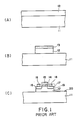
- FIGS.1(A) - (C) show a typical prior art process for manufacturing a metal-oxide-silicon field effect transistor (MOSFET) on a silicon carbide layer.
- MOSFET metal-oxide-silicon field effect transistor
- FIG.1(A) a silicon carbide layer 12 is grown on a silicon substrate 11 by chemical vapor deposition, and after deposition of aluminium layer 13 on the silicon carbide layer 12 and a subsequent patterning for exposing the silicon carbide layer 12 except for a device region in which the semiconductor device is to be formed, the structure is etched in a nitrogen trifluoride (NF3) etching gas and a structure shown in FIG.1(B) is obtained.
- NF3 nitrogen trifluoride
- a MOS structure comprising a gate oxide film 14, a gate electrode 15, source and drain regions 16 and 17, and source and drain electrodes 18 are formed by a well known process. Further, an aluminium interconnection 20 is provided on the substrate 11 so as to make a contact with the source and drain electrodes 18 and a MOSFET shown in FIG.1(C) is obtained.
- the MOSFET thus obtained has a problem in that the manufacturing process is complex as it involves the step of forming the mesa structure. Further, the integration density is limited because of the separation between the mesa structures. Associated with use of the mesa structure, there arises a further problem in that a leakage current flowing through a side wall of the mesa structure is increased because of minute projections and depressions formed on the side wall at the time of etching. It is believed that such minute projections and depressions facilitate adsorption of impurities on the side wall of the mesa structure and thus provide a path for the leakage current.
- the steep side wall of the mesa structure tends to cause a disconnection of the metal interconnection 20 particularly at a part 19 along the side wall where the thickness of the interconnection is thin.
- the disconnection of the metal interconnection 20 is facilitated further by the minute projections and depressions on the side wall.
- Another and more specific object of the present invention is to provide a method of manufacturing a semiconductor device having a silicon carbide layer, comprising steps of introducing an impurity into a silicon carbide layer in correspondence to a region in which a device isolation structure is to be formed, and selectively oxidizing said region by annealing the device in an atmosphere containing oxygen.
- the region in which the impurity is introduced is selectively oxidized and there is formed a thick silicon oxide in correspondence to the device isolation structure.
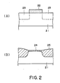
- FIGS.2(A) and (B) show the principle of the present invention.
- a part of a silicon carbide substrate 21 on which a semiconductor device is to be formed is covered by a photoresist 22 and an impurity such as phosphorus (P), boron (B), arsenic (As) or compound of these elements is introduced into an uncovered part of the silicon carbide substrate.
- an impurity region 23 doped with the impurity is formed.
- the photoresist 22 is removed and the structure of FIG.2(A) is subjected to thermal oxidation.
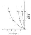
- FIG.3 shows a result of experiment conducted to evaluate the oxidation rate of silicon carbide doped to various dopant concentration levels.
- the experiment was conducted on a specimen of silicon carbide in which B is introduced by ion implantation with an acceleration voltage of 80 keV.
- the specimen was further heat treated in a reaction vessel (not shown) under an atmosphere containing oxygen at 1050 °C.
- the oxygen partial pressure was controlled by flowing oxygen and hydrogen into the reaction vessel such that there is established a water vapor pressure of 760 Torr in the reaction vessel.
- the curve I represents a case in which boron ion (B+) is introduced by ion implantation with a dose of 5 X 1012 cm ⁇ 2
- the curve II represents a case in which the dose is 1 X 1014 cm ⁇ 2
- the curve III represents a case in which the dose is 1 X 1015 cm ⁇ 2.
- the rate of oxidation represented by the thickness of silicon oxide film grown on the silicon carbide, is increased with increasing concentration of B in the specimen.
- the thickness of the silicon oxide film after the heat treatment for one hour is summarized in the following Table I . TABLE I relation between oxidation rate and dose of boron in silicon carbide dose (cm ⁇ 2) SiO2 thickness (nm) 5 X 10¹² 20 1 X 10¹⁴ 100 1 X 10¹⁵ 250
- the oxidation rate of undoped or pure silicon carbide measured in the temperature range of 950 - 1150°C is only about 4 - 8 % of that of silicon while when the impurity such as B , P , As or compound of these elements is introduced with a concentration level of more than about 1 X 1019 cm ⁇ 3, the oxidation rate increases to as much as 40 - 60 % of that of silicon.
- a thick oxide layer 25 is formed in the impurity region 23 because of the increased oxidation rate.
- a thin oxide layer 24 in the part of the substrate 21 on which the device is to be formed.
- an oxide layer having a thickness of 400 - 800 nm and a breakdown voltage of 6 - 10 MV/cm is obtained by oxidation for two through four hours.
- the semiconductor device is a MOSFET.
- a layer 32 of ⁇ - phase silicon carbide (referred to hereinafter as ⁇ -SiC) is grown on a (111) surface of an n-type silicon substrate 31 having a resistivity of 1 - 10 ⁇ -cm by chemical vapor deposition.
- the growth is made by introducing trichlorosilane (SiHCl3) and propane (C3H8) into a reactor (not shown) as source gases.
- SiHCl3 trichlorosilane
- propane C3H8
- the introduction of the source gas is performed by bubbling using hydrogen (H2).
- the growth is made at a reduced pressure of 3.0 Torr and a temperature of 1000°C.
- the flow rate of SiHCl3, C3H8 and H2 is adjusted such that the partial pressure of SiHCl3, C3H8 and H2 are respectively 3.57 X 10 ⁇ 4 Torr, 1.53 X 10 ⁇ 5 Torr, and 3.57 X 10 ⁇ 3 Torr.
- a diborane (B2H6) gas is added to the source gas so that the obtained silicon carbide layer 32 is doped to the p-type and has a resistivity of 1 - 10 ⁇ cm.
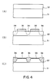
- a photoresist 33 is applied on the SiC layer 32 in correspondence to a region in which the semiconductor device is to be formed and the structure thus obtained is subjected to ion implantation of phosphorus ion (P+) using the photoresist 33 as a mask.
- the ion implantation is made under an acceleration voltage of 80 - 120 keV with a dose of 1014 - 1015 cm ⁇ 2 and thus an impurity region 34 is formed in correspondence to the device isolation structure as shown in FIG.4(B).
- FIG.4(B) After the removal of the photoresist 33, the structure of FIG.4(B) is oxidized in a thermal oxidation furnace at 1050°C for two hours under one atmosphere while flowing oxygen and hydrogen such that the partial pressure of water vapor (H2O) formed in the furnace is maintained at about 760 Torr.
- H2O water vapor
- FIG.4(C) a thin oxide layer 35 is formed in correspondence to the region protected by the photoresist against ion implantation.
- a thick oxide layer 36 in correspondence to the impurity region 34 with a thickness of about 400 - 600 nm.
- a polysilicon layer is deposited on the thin oxide layer 35 and after suitable patterning to form a gate electrode 37 as shown in FIG.4(D), a source region 38 and a drain region 39 are formed by ion implantation of P+ using the gate electrode 37 as well as the thick oxide layer 36 as the mask. Further, the surface of the gate electrode 37 is oxidized and an oxide film 40 covering the gate electrode 37 is formed.
- a phosphosilicate glass (PSG) layer 41 is deposited on the structure of FIG.4(D) as an interlayer insulator and contact holes are provided on the PSG layer 41 as well as on the silicon oxide layers 35 and 40 existing under the layer 41, in correspondence to the source region 38, drain region 39 and the gate electrode 37.
- PSG phosphosilicate glass
- the oxidation rate of the SiC 32 is selectively enhanced by introducing the impurity with a large dosage and the thick oxide layer 35 is formed exactly in correspondence to the device isolation structure. Further, by changing the energy of ion implantation, the thickness of the oxide layer 35 is controlled easily.
- the MOSFET obtained by the process of the present invention has the planer structure, the step of providing the mesa structure as well as the step for obtaining a flat top surface suitable for interlayer connection is eliminated and the manufacturing process is significantly simplified. Associated therewith, the degree of integration can be increased and the leakage current is minimized.
- the semiconductor device is a bipolar transistor.
- an n+-type ⁇ -SiC layer 52 and an n-type ⁇ -SiC layer 53 are grown successively on a silicon substrate 51 similarly to the first embodiment with a thickness of 3000 ⁇ for the layer 52 and 2000 ⁇ for the layer 53.
- phosphine (PH3) is added to the source gas with a partial pressure of 1.02 X 10 ⁇ 8 Torr and a partial pressure of 1.53 X 10 ⁇ 10 Torr respectively so that the layer 52 and the layer 53 are doped to a carrier concentration level of 5 X 1018 cm ⁇ 3 and 1 X 1017 cm ⁇ 3.
- FIG.5(A) shows a structure obtained by the foregoing procedures.
- B+ is introduced to the exposed part 53a of the SiC layer 53 by ion implantation under an acceleration voltage of 400 keV with a dose of about 5 X 10¹⁴/cm ⁇ 2 to about 1 X 10¹⁵/cm ⁇ 2. Further, the structure thus processed is annealed at 1100°C, one atmosphere with a H2O partial pressure of 760 Torr and a device isolation oxide layer 55 is formed. Note that the device isolation oxide layer 55 thus formed includes a large thickness region 55a having a thickness corresponding to the total thickness of the SiC layers 52 and 53 at the region in which the ion implantation of B+ is made and a small thickness region 55b in correspondence to the region in which the ion implantation is not made.
- the structure thus obtained is further applied with a photoresist 56 which is subsequently patterned so as to expose a part 55c of the thin oxide region 55b at both sides of the emitter to be formed in the structure.
- a structure shown in FIG.5(B) is obtained.
- FIG.5(C) After injecting B+ under an acceleration voltage of 100 keV with a dose of 5 X 10¹⁴ - 1 X 1015 cm ⁇ 2, the structure of FIG.5(C) is heat treated similarly to the foregoing case and a pair of oxide regions 55d as shown in FIG.5(C) are formed.
- FIG.5(C) is further deposited with a thin silicon nitride layer 57 by chemical vapor deposition and a part of the layer 57 corresponding to the emitter and the base of the bipolar transistor is selectively removed by etching. After the etching, a part of the silicon oxide layer 55b underlying the removed part of the layer 57 is further etched and a p-type ⁇ -SiC layer 58 is subsequently grown so as to make a contact with a part of the SiC layer 53 exposed by the foregoing etching process for a thickness of about 500 - 1000 ⁇ .
- the growth of the SiC layer 58 is performed similarly to the case of growing the layers 52 and 53 except that B2H6 or trimethyl boron is added to the source gas such that the SiC layer 58 is doped to the p-type with a hole concentration level of about 5 X 1019 cm ⁇ 3.
- the partial pressure of B2H6 is set to 1 - 5 X 10 ⁇ 7 Torr.
- the partial pressure is set to 3 - 5 X 10 ⁇ 8 Torr.
- the SiC layer 58 is further removed selectively by plasma etching using nitrogen trifluoride NF3 so that only a part of the layer 58 corresponding to the base of the bipolar transistor and making a direct contact with the exposed part of the SiC layer 53 is left as illustrated in FIG.5(D).
- a silicon oxide layer 59 is deposited on the structure of FIG.5(D) by chemical vapor deposition and a contact hole 59a is provided so as to expose the foregoing part of the SiC layer 58 in contact with the layer 53.
- an n+-type SiC layer 60 is grown on the SiC layer 58 in correspondence to the contact hole 59a for a thickness of about 2000 ⁇ by a process similar to that used for growing the layers 52 and 53, except that the partial pressure for PH3 is set to 1.02 X 10 ⁇ 7 Torr so that a carrier concentration level of about 5 X 1019 cm ⁇ 3 is obtained.
- the layer 60 is then patterned so that only a part thereof corresponding to the emitter of the transistor is left on the part of the layer 58 making a direct contact with the underlying SiC layer 53. Further, after formation of the contact holes 59b and 59c for the base and emitter of the bipolar transistor, aluminium is deposited so as to fill the contact holes 59a - 59c and the bipolar transistor is completed.
- the selective oxidation of SiC facilitates the formation of the device isolation structure.
- the bipolar transistor can be formed by a simple procedure without providing the mesa structure.
- the process for introducing the impurity into the silicon carbide layer described heretofore is ion implantation, the present invention is not limited as such but solid diffusion process or vapor phase diffusion process can be employed similarly for this purpose.
- the impurity to be introduced into silicon carbide for selective oxidation is not limited to B and P , but As may be used with substantially a same result.
- the substrate 21, 31 or 51 is not limited to silicon single crystal but may be a bulk silicon carbide or a silicon epitaxial layer grown of an insulator such as sapphire.
Landscapes
- Formation Of Insulating Films (AREA)
- Local Oxidation Of Silicon (AREA)
- Element Separation (AREA)
- Insulated Gate Type Field-Effect Transistor (AREA)
Applications Claiming Priority (2)
| Application Number | Priority Date | Filing Date | Title |
|---|---|---|---|
| JP63254898A JP2670563B2 (ja) | 1988-10-12 | 1988-10-12 | 半導体装置の製造方法 |
| JP254898/88 | 1988-10-12 |
Publications (2)
| Publication Number | Publication Date |
|---|---|
| EP0363944A1 true EP0363944A1 (de) | 1990-04-18 |
| EP0363944B1 EP0363944B1 (de) | 1996-08-28 |
Family
ID=17271377
Family Applications (1)
| Application Number | Title | Priority Date | Filing Date |
|---|---|---|---|
| EP89118919A Expired - Lifetime EP0363944B1 (de) | 1988-10-12 | 1989-10-11 | Verfahren zur Herstellung eines Halbleiterbauelementes, das eine Siliciumcarbidschicht besitzt |
Country Status (4)
| Country | Link |
|---|---|
| US (1) | US4994413A (de) |
| EP (1) | EP0363944B1 (de) |
| JP (1) | JP2670563B2 (de) |
| DE (1) | DE68927032D1 (de) |
Cited By (11)
| Publication number | Priority date | Publication date | Assignee | Title |
|---|---|---|---|---|
| US5135885A (en) * | 1989-03-27 | 1992-08-04 | Sharp Corporation | Method of manufacturing silicon carbide fets |
| EP0637069A1 (de) * | 1992-06-05 | 1995-02-01 | Cree Research, Inc. | Verfahren zur Erzeugung von Silizium-Dioxid-Passivierung hoher Qualität auf Silizium-Carbid und resultierende passivierte Strukturen |
| EP0635881A3 (de) * | 1993-07-12 | 1995-10-11 | Motorola Inc | Verfahren zur Herstellung eines vertikalen LOCOS-MOSFET aus Siliziumkarbid und Anordnung. |
| US5612260A (en) * | 1992-06-05 | 1997-03-18 | Cree Research, Inc. | Method of obtaining high quality silicon dioxide passivation on silicon carbide and resulting passivated structures |
| WO2001072104A1 (es) * | 2000-03-31 | 2001-10-04 | Consejo Superior De Investigaciones Científicas | Procedimiento de fabricación de capas de carburo de silicio (sic) mediante implantación iónica de carbono y recocidos |
| EP1237185A3 (de) * | 2001-02-20 | 2003-07-30 | STMicroelectronics S.r.l. | Verfahren zur Herstellung isolierender Strukturen |
| US7543377B2 (en) | 1996-03-28 | 2009-06-09 | Intel Corporation | Perimeter matrix ball grid array circuit package with a populated center |
| US8269931B2 (en) | 2009-09-14 | 2012-09-18 | The Aerospace Corporation | Systems and methods for preparing films using sequential ion implantation, and films formed using same |
| US8946864B2 (en) | 2011-03-16 | 2015-02-03 | The Aerospace Corporation | Systems and methods for preparing films comprising metal using sequential ion implantation, and films formed using same |
| US9324579B2 (en) | 2013-03-14 | 2016-04-26 | The Aerospace Corporation | Metal structures and methods of using same for transporting or gettering materials disposed within semiconductor substrates |
| EP3682464A4 (de) * | 2017-09-13 | 2021-06-09 | University of Technology Sydney | Elektrische isolationsstruktur und verfahren |
Families Citing this family (22)
| Publication number | Priority date | Publication date | Assignee | Title |
|---|---|---|---|---|
| JP2542448B2 (ja) * | 1990-05-24 | 1996-10-09 | シャープ株式会社 | 電界効果トランジスタおよびその製造方法 |
| US5821563A (en) | 1990-12-25 | 1998-10-13 | Semiconductor Energy Laboratory Co., Ltd. | Semiconductor device free from reverse leakage and throw leakage |
| US7253437B2 (en) * | 1990-12-25 | 2007-08-07 | Semiconductor Energy Laboratory Co., Ltd. | Display device having a thin film transistor |
| US5264713A (en) * | 1991-06-14 | 1993-11-23 | Cree Research, Inc. | Junction field-effect transistor formed in silicon carbide |
| JPH0529621A (ja) * | 1991-07-19 | 1993-02-05 | Rohm Co Ltd | 炭化珪素薄膜回路素子とその製造方法 |
| US6344663B1 (en) | 1992-06-05 | 2002-02-05 | Cree, Inc. | Silicon carbide CMOS devices |
| US5726463A (en) * | 1992-08-07 | 1998-03-10 | General Electric Company | Silicon carbide MOSFET having self-aligned gate structure |
| JP3146694B2 (ja) * | 1992-11-12 | 2001-03-19 | 富士電機株式会社 | 炭化けい素mosfetおよび炭化けい素mosfetの製造方法 |
| US5270244A (en) * | 1993-01-25 | 1993-12-14 | North Carolina State University At Raleigh | Method for forming an oxide-filled trench in silicon carbide |
| US5448081A (en) * | 1993-02-22 | 1995-09-05 | Texas Instruments Incorporated | Lateral power MOSFET structure using silicon carbide |
| US5385855A (en) * | 1994-02-24 | 1995-01-31 | General Electric Company | Fabrication of silicon carbide integrated circuits |
| US5972801A (en) * | 1995-11-08 | 1999-10-26 | Cree Research, Inc. | Process for reducing defects in oxide layers on silicon carbide |
| US5719409A (en) * | 1996-06-06 | 1998-02-17 | Cree Research, Inc. | Silicon carbide metal-insulator semiconductor field effect transistor |
| JPH11251592A (ja) * | 1998-01-05 | 1999-09-17 | Denso Corp | 炭化珪素半導体装置 |
| US6303508B1 (en) | 1999-12-16 | 2001-10-16 | Philips Electronics North America Corporation | Superior silicon carbide integrated circuits and method of fabricating |
| US6656811B2 (en) * | 2001-12-21 | 2003-12-02 | Texas Instruments Incorporated | Carbide emitter mask etch stop |
| US7012007B1 (en) * | 2003-09-09 | 2006-03-14 | Advanced Micro Device, Inc. | Strained silicon MOSFET having improved thermal conductivity and method for its fabrication |
| US7015111B2 (en) * | 2003-10-28 | 2006-03-21 | Micron Technology, Inc. | Use of selective oxidation to form asymmetrical oxide features during the manufacture of a semiconductor device |
| US7932111B2 (en) * | 2005-02-23 | 2011-04-26 | Cree, Inc. | Substrate removal process for high light extraction LEDs |
| US20070096107A1 (en) * | 2005-11-03 | 2007-05-03 | Brown Dale M | Semiconductor devices with dielectric layers and methods of fabricating same |
| US20080054270A1 (en) * | 2006-09-05 | 2008-03-06 | Yoshiyuki Suda | Semiconductor memory device and the production method |
| EP3843768A4 (de) | 2018-05-15 | 2022-11-23 | Tran, Lloyd Hung Loi | Therapeutikumzusammensetzung und verfahren zur verwendung, zur behandlung von leichter kognitiver beeinträchtigung, depressionen und psychischen störungen |
Citations (2)
| Publication number | Priority date | Publication date | Assignee | Title |
|---|---|---|---|---|
| DE3446961A1 (de) * | 1983-12-23 | 1985-07-18 | Sharp K.K., Osaka | Verfahren zur herstellung einer sic-halbleitervorrichtung |
| US4757028A (en) * | 1985-10-07 | 1988-07-12 | Agency Of Industrial Science And Technology | Process for preparing a silicon carbide device |
Family Cites Families (2)
| Publication number | Priority date | Publication date | Assignee | Title |
|---|---|---|---|---|
| US3662458A (en) * | 1969-06-20 | 1972-05-16 | Westinghouse Electric Corp | Electrical contact for silicon carbide members |
| JPS5987831A (ja) * | 1982-11-12 | 1984-05-21 | Hitachi Ltd | 半導体装置の製造方法 |
-
1988
- 1988-10-12 JP JP63254898A patent/JP2670563B2/ja not_active Expired - Fee Related
-
1989
- 1989-10-11 DE DE68927032T patent/DE68927032D1/de not_active Expired - Lifetime
- 1989-10-11 EP EP89118919A patent/EP0363944B1/de not_active Expired - Lifetime
- 1989-10-12 US US07/420,465 patent/US4994413A/en not_active Expired - Lifetime
Patent Citations (2)
| Publication number | Priority date | Publication date | Assignee | Title |
|---|---|---|---|---|
| DE3446961A1 (de) * | 1983-12-23 | 1985-07-18 | Sharp K.K., Osaka | Verfahren zur herstellung einer sic-halbleitervorrichtung |
| US4757028A (en) * | 1985-10-07 | 1988-07-12 | Agency Of Industrial Science And Technology | Process for preparing a silicon carbide device |
Non-Patent Citations (1)
| Title |
|---|
| IEEE ELECTRON DEVICE LETTERS, vol. EDL-7, no. 12, December 1986, pages 692-693, IEEE, New York, US; K. SHIBAHARA et al.: "Fabrication of inversion-type n-channel MOSFET's using cubic-SiC on Si(100)" * |
Cited By (18)
| Publication number | Priority date | Publication date | Assignee | Title |
|---|---|---|---|---|
| US5135885A (en) * | 1989-03-27 | 1992-08-04 | Sharp Corporation | Method of manufacturing silicon carbide fets |
| EP0637069A1 (de) * | 1992-06-05 | 1995-02-01 | Cree Research, Inc. | Verfahren zur Erzeugung von Silizium-Dioxid-Passivierung hoher Qualität auf Silizium-Carbid und resultierende passivierte Strukturen |
| US5459107A (en) * | 1992-06-05 | 1995-10-17 | Cree Research, Inc. | Method of obtaining high quality silicon dioxide passivation on silicon carbide and resulting passivated structures |
| US5612260A (en) * | 1992-06-05 | 1997-03-18 | Cree Research, Inc. | Method of obtaining high quality silicon dioxide passivation on silicon carbide and resulting passivated structures |
| US5629531A (en) * | 1992-06-05 | 1997-05-13 | Cree Research, Inc. | Method of obtaining high quality silicon dioxide passivation on silicon carbide and resulting passivated structures |
| US5776837A (en) * | 1992-06-05 | 1998-07-07 | Cree Research, Inc. | Method of obtaining high quality silicon dioxide passivation on silicon carbide and resulting passivated structures |
| EP0635881A3 (de) * | 1993-07-12 | 1995-10-11 | Motorola Inc | Verfahren zur Herstellung eines vertikalen LOCOS-MOSFET aus Siliziumkarbid und Anordnung. |
| US7543377B2 (en) | 1996-03-28 | 2009-06-09 | Intel Corporation | Perimeter matrix ball grid array circuit package with a populated center |
| ES2165315A1 (es) * | 2000-03-31 | 2002-03-01 | Consejo Superior Investigacion | Procedimiento de fabricacion de capas de carburo de silicio (sic) mediante implantacion ionica de carbono y recocidos. |
| WO2001072104A1 (es) * | 2000-03-31 | 2001-10-04 | Consejo Superior De Investigaciones Científicas | Procedimiento de fabricación de capas de carburo de silicio (sic) mediante implantación iónica de carbono y recocidos |
| EP1237185A3 (de) * | 2001-02-20 | 2003-07-30 | STMicroelectronics S.r.l. | Verfahren zur Herstellung isolierender Strukturen |
| US6762112B2 (en) | 2001-02-20 | 2004-07-13 | Stmicroelectronics S.R.L. | Method for manufacturing isolating structures |
| US8269931B2 (en) | 2009-09-14 | 2012-09-18 | The Aerospace Corporation | Systems and methods for preparing films using sequential ion implantation, and films formed using same |
| US9048179B2 (en) | 2009-09-14 | 2015-06-02 | The Aerospace Corporation | Systems and methods for preparing films using sequential ion implantation, and films formed using same |
| US8946864B2 (en) | 2011-03-16 | 2015-02-03 | The Aerospace Corporation | Systems and methods for preparing films comprising metal using sequential ion implantation, and films formed using same |
| US9324579B2 (en) | 2013-03-14 | 2016-04-26 | The Aerospace Corporation | Metal structures and methods of using same for transporting or gettering materials disposed within semiconductor substrates |
| EP3682464A4 (de) * | 2017-09-13 | 2021-06-09 | University of Technology Sydney | Elektrische isolationsstruktur und verfahren |
| US11348824B2 (en) | 2017-09-13 | 2022-05-31 | University Of Technology Sydney | Electrical isolation structure and process |
Also Published As
| Publication number | Publication date |
|---|---|
| JPH02102557A (ja) | 1990-04-16 |
| EP0363944B1 (de) | 1996-08-28 |
| DE68927032D1 (de) | 1996-10-02 |
| JP2670563B2 (ja) | 1997-10-29 |
| US4994413A (en) | 1991-02-19 |
Similar Documents
| Publication | Publication Date | Title |
|---|---|---|
| EP0363944B1 (de) | Verfahren zur Herstellung eines Halbleiterbauelementes, das eine Siliciumcarbidschicht besitzt | |
| US4462847A (en) | Fabrication of dielectrically isolated microelectronic semiconductor circuits utilizing selective growth by low pressure vapor deposition | |
| US3370995A (en) | Method for fabricating electrically isolated semiconductor devices in integrated circuits | |
| US3861968A (en) | Method of fabricating integrated circuit device structure with complementary elements utilizing selective thermal oxidation and selective epitaxial deposition | |
| US4749441A (en) | Semiconductor mushroom structure fabrication | |
| US4493740A (en) | Method for formation of isolation oxide regions in semiconductor substrates | |
| EP0068154B1 (de) | Integrierte Schaltung mit einem Halbleitersubstrat mit Isolationszonen und elektrisch leitenden Zonen | |
| EP0442718A2 (de) | Verfahren zum Herstellen einer Halbleitervorrichtung | |
| Anner | Planar processing primer | |
| EP0036573A2 (de) | Verfahren zur Herstellung einer Polysilicium-Leiterstruktur | |
| EP0227085A2 (de) | Verfahren zum Herstellen von IGFETs mit minimaler Übergangstiefe durch epitaktische Rekristallisation | |
| JPS592187B2 (ja) | 導電層間に絶縁物を形成する方法 | |
| EP0076106B1 (de) | Verfahren zur Herstellung eines bipolaren Transistors | |
| GB1587398A (en) | Semiconductor device manufacture | |
| CA1208805A (en) | Vertically isolated complementary transistors | |
| US3883889A (en) | Silicon-oxygen-nitrogen layers for semiconductor devices | |
| EP0111706B1 (de) | Seitenwandisolation der Gate-Elektrode von Feldeffekttransistoren und Verfahren zu ihrer Herstellung | |
| US4140547A (en) | Method for manufacturing MOSFET devices by ion-implantation | |
| US4159561A (en) | Method of making a substrate contact for an integrated circuit | |
| US4210689A (en) | Method of producing semiconductor devices | |
| US3494809A (en) | Semiconductor processing | |
| JPS6133253B2 (de) | ||
| US3702790A (en) | Monolithic integrated circuit device and method of manufacturing the same | |
| GB1572819A (en) | Semiconductor device | |
| US3574007A (en) | Method of manufacturing improved mis transistor arrays |
Legal Events
| Date | Code | Title | Description |
|---|---|---|---|
| PUAI | Public reference made under article 153(3) epc to a published international application that has entered the european phase |
Free format text: ORIGINAL CODE: 0009012 |
|
| AK | Designated contracting states |
Kind code of ref document: A1 Designated state(s): DE FR GB |
|
| 17P | Request for examination filed |
Effective date: 19900627 |
|
| 17Q | First examination report despatched |
Effective date: 19920304 |
|
| GRAH | Despatch of communication of intention to grant a patent |
Free format text: ORIGINAL CODE: EPIDOS IGRA |
|
| GRAH | Despatch of communication of intention to grant a patent |
Free format text: ORIGINAL CODE: EPIDOS IGRA |
|
| GRAA | (expected) grant |
Free format text: ORIGINAL CODE: 0009210 |
|
| AK | Designated contracting states |
Kind code of ref document: B1 Designated state(s): DE FR GB |
|
| REF | Corresponds to: |
Ref document number: 68927032 Country of ref document: DE Date of ref document: 19961002 |
|
| ET | Fr: translation filed | ||
| PG25 | Lapsed in a contracting state [announced via postgrant information from national office to epo] |
Ref country code: GB Effective date: 19961128 |
|
| PG25 | Lapsed in a contracting state [announced via postgrant information from national office to epo] |
Ref country code: DE Effective date: 19961129 |
|
| PLBE | No opposition filed within time limit |
Free format text: ORIGINAL CODE: 0009261 |
|
| STAA | Information on the status of an ep patent application or granted ep patent |
Free format text: STATUS: NO OPPOSITION FILED WITHIN TIME LIMIT |
|
| GBPC | Gb: european patent ceased through non-payment of renewal fee |
Effective date: 19961128 |
|
| 26N | No opposition filed | ||
| PGFP | Annual fee paid to national office [announced via postgrant information from national office to epo] |
Ref country code: FR Payment date: 20051010 Year of fee payment: 17 |
|
| REG | Reference to a national code |
Ref country code: FR Ref legal event code: ST Effective date: 20070629 |
|
| PG25 | Lapsed in a contracting state [announced via postgrant information from national office to epo] |
Ref country code: FR Free format text: LAPSE BECAUSE OF NON-PAYMENT OF DUE FEES Effective date: 20061031 |