EP0364314A1 - Verfahren zum Lesen von lichtempfindlichen Zellen mit zwei in Reihe angeordneten Dioden und mit entgegenwirkenden Durchlassrichtungen - Google Patents
Verfahren zum Lesen von lichtempfindlichen Zellen mit zwei in Reihe angeordneten Dioden und mit entgegenwirkenden Durchlassrichtungen Download PDFInfo
- Publication number
- EP0364314A1 EP0364314A1 EP89402483A EP89402483A EP0364314A1 EP 0364314 A1 EP0364314 A1 EP 0364314A1 EP 89402483 A EP89402483 A EP 89402483A EP 89402483 A EP89402483 A EP 89402483A EP 0364314 A1 EP0364314 A1 EP 0364314A1
- Authority
- EP
- European Patent Office
- Prior art keywords
- reading
- photosensitive
- voltage
- diode
- illumination
- Prior art date
- Legal status (The legal status is an assumption and is not a legal conclusion. Google has not performed a legal analysis and makes no representation as to the accuracy of the status listed.)
- Granted
Links
Images

Classifications
-
- H—ELECTRICITY
- H04—ELECTRIC COMMUNICATION TECHNIQUE
- H04N—PICTORIAL COMMUNICATION, e.g. TELEVISION
- H04N25/00—Circuitry of solid-state image sensors [SSIS]; Control thereof
- H04N25/60—Noise processing, e.g. detecting, correcting, reducing or removing noise
-
- H—ELECTRICITY
- H04—ELECTRIC COMMUNICATION TECHNIQUE
- H04N—PICTORIAL COMMUNICATION, e.g. TELEVISION
- H04N25/00—Circuitry of solid-state image sensors [SSIS]; Control thereof
- H04N25/70—SSIS architectures; Circuits associated therewith
- H04N25/76—Addressed sensors, e.g. MOS or CMOS sensors
Definitions
- the invention relates to the field of reading photosensitive cells, in particular of the solid state type, and where each cell comprises two diodes mounted in series and mounted head to tail, that is to say with directions of opposite conduction, at least one of these two diodes being a photodiode.
- the object of the process of the invention is particularly to increase the reading speed while retaining the required precision and quality at this reading, particularly in the case where the photosensitive cell has been exposed to a useful signal of low intensity.
- a photosensitive matrix includes an array of in-line conductors and an array of columnar conductors.
- a photosensitive assembly or photosensitive cell is called a photosensitive point in the following description; the photosensitive points are thus also organized in rows and columns.
- Each photosensitive point is connected between a row conductor and a column conductor: in fact to each row conductor are connected as many photosensitive points as there are columns of the latter, and to each conductor in column are connected as many photosensitive points as 'there are lines of these.
- the number of photosensitive points in a given surface determines the resolution of the image. He is known to make arrays of large-capacity photosensitive elements, for example 2000 x 2000 photosensitive dots, to obtain an image whose dimensions are of the order of 40 cm x 40 cm. In this case, each photosensitive point is located in an elementary surface area whose maximum dimensions are 200 micrometers x 200 micrometers. Such an arrangement makes it possible to constitute surface type detectors which can be applied in particular to radiology, provided that a scintillator is added, to the detection of particles (electrons, neutrons, etc.) and to reprography.
- Each photosensitive point includes a photosensitive element such as photodiode, phototransistor, sensitive to visible or near visible light photons. These light photons are converted into electric charge, and this electric charge is accumulated in an electric capacity forming a storage capacity, which can be constituted by the capacity of the photosensitive element itself.
- a reading device makes it possible to interrogate the electrical state of the storage capacity, and to convey the electrical charge which constitutes the signal to a signal amplifier.
- One of the main problems with reading photosensitive dots is that the electrical capacity presented by photosensitive cells is too high. The influence of this capacity is exerted particularly when reading photosensitive points, that is to say during the amplification of the photocharge developed by a photosensitive element, a photodiode for example following its illumination. This capacity of each photosensitive element is applied to the column conductors and to the sense amplifier to which this element is connected, and tends to deteriorate the signal / noise ratio.
- each photosensitive cell includes an element acting as a switch held in the open state, except in the reading phase of the photosensitive cell to which it belongs.
- a diode mounted in series with the photosensitive element.
- the reading method used is such that the first diode functions as a switch which is set to the closed state only during the reading phase of the cells connected to the line conductor to which it belongs; this results in good decoupling of the column conductors with respect to the photosensitive cells of the unaddressed lines.
- a photosensitive cell formed by an assembly of two diodes in series, head to tail, and the operation of which is obtained by a conventional reading method as described in the document mentioned above has certain significant drawbacks, and particularly the 'disadvantage of introducing an error which can be considerable on the reading of the charges generated at a photosensitive point during the exposure of the latter to a light signal to be captured; this defect being all the more pronounced when the signal is weak and when one seeks to obtain a high reading speed.
- the method of the invention avoids these drawbacks and applies to the reading of photosensitive dots or cells comprising two diodes mounted in head-to-tail series as has been explained above.
- a method of reading at least one photosensitive point comprising first and second diodes connected in series with opposite directions of conduction, at least one of the diodes being photosensitive, said method consisting in polarizing the two diodes by - inverse during the exposure of the photosensitive point to a useful signal, so as to accumulate a quantity of signal charges in a floating potential area located at the connection of the two diodes, then to polarize the first diode live during reading phases by periodic read pulses, said method being characterized in that it further consists in illuminating the photosensitive point by additional illumination in order to generate in the floating potential area training charges which add at least partially to the signal load.
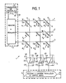
- Figure 1 shows by way of nonlimiting example, the electrical diagram of a photosensitive matrix 1; this electrical diagram being in itself conventional: in fact the matrix comprises a plurality of photosensitive points P1 to P9 each consisting of photosensitive cells as described in the French patent application No. 86 14058 previously cited, that is to say -to say that each photosensitive point P1, P9 or cell is formed by two diodes Da, Db connected in series, and head to tail, that is to say with opposite directions of conduction.
- the number of photosensitive points P1 to P9 is limited to 9, according to a 3 ⁇ 3 matrix assembly to simplify FIG. 1, but in the spirit of the invention this matrix assembly can have a capacity much larger, by several million points for example.
- the matrix 1 comprises in-line conductors L1 to L3 and in column conductors F1 to F3, the number of each type of these conductors being limited to three, taking into account the example of the figure where only 9 photosensitive points P1 to P9 are represented.
- the photosensitive points P1 to P9 are each formed at the intersection of a line conductor L1 to L3 and a column conductor F1 to F3.
- Each photosensitive point P1 to P9 has a first end 10 connected to an in-line conductor L1 to L3, and has a second end 11 connected to a column conductor F1 to F3.
- the first diode Da is connected to a line conductor L1 to L3 by its anode which forms the first end 10
- the second diode Db is connected to a column conductor F1 to F3 also by its anode which forms the second end 11.
- Each of the diodes Da, Db constitutes in known manner, a capacitor Ca, Cb when this diode is reverse biased; and in the case of photosensitive points P1 to P9, the capacitance Cb of the second diodes Db is approximately 10 times greater than the capacitance Ca of the first diodes Da; the first Da diodes having to fulfill mainly a switch function as taught by the patent application already mentioned.
- the line conductors L1 to L3 are connected to a line 2 addressing device comprising in particular a logic shift register 3 which makes it possible to ensure the sequential addressing of each line L1 to L3 with a view to reading the photosensitive points P1 to P9 which are connected to this line.
- Register 3 makes it possible to apply a voltage VL in the form of a pulse called read pulse IL, from line conductor to line conductor, while the other unaddressed line conductors are maintained at a reference potential VR.
- the read voltage pulses IL are supplied by a voltage pulse generator 6 whose output 7 is for this purpose connected to the shift register 3, and of which another output 8 is connected to the reference voltage VR which is the mass in the nonlimiting example described.
- the read pulses IL make it possible to read the photosensitive points P1 to P9, that is to say to transfer to the column conductors charges generated by an illumination signal or useful signal (not shown) to which each point can be exposed photosensitive: these charges, which are proportional to the intensity of the illumination, are stored in an area formed at the connection between the two diodes Da and Db of each photosensitive point P1 to P9, this area or connection between these two diodes being symbolized in the figure by a point marked A and constitutes a point with floating potential, because its potential varies with the quantity of charges which accumulate there; this amount of charge can be generated by one or the other of the two diodes Da, Db or by these two diodes depending on whether they are one and / or the other photosensitive. But preferably it is the second diode Db, which has the highest capacity, which must be photosensitive, while the first diode Da, the main function of which is that of a switch, may possibly not be photosensitive.
- each column conductor F1 to F3 is connected to the negative input "-" of an operational amplifier G1 to G3, mounted as an integrator using an integration capacitor CL1 to CL3.
- Each integration capacitor is mounted between the negative input "-” of the amplifier G1 to G3 and the output OF1, OF2, OF3 of the latter.
- the second input or positive input "+” of each amplifier G1 to G3 is connected to a column reference potential which imposes on each column conductor F1 to F3 this reference potential.
- This potential may or may not be the same potential VR as that of the line addressing device. In what follows we will consider, for simplicity, that the reference potential is the same for the rows and the columns.
- Each integrated amplifier G1, G3 comprises a reset switch I1 to I3 mounted in parallel with the integration capacitor CL1 to CL3; in figure 1 of switches I1 to I3 are represented according to switches, but they can of course be constituted in a conventional manner by transistors, of the MOS type for example, controlled by reset signals (not shown).
- the outputs OF1 to OF3 of amplifier G1 to G3 are connected to reading and multiplexing means 9, comprising for example an analog data acquisition device 4 formed by a shift register with parallel input and S serial output, CCD type for example (from the English term "Charge Coupled Device").
- the analog data acquisition device 9 can thus output in series, in a conventional manner, signals (not shown) which correspond to the charges which have been integrated by the amplifiers G1 to G3 and in the reading phase of all the photosensitive points connected to the same line conductor L1 to L3.
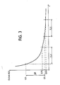
- FIGS. 2a to 2e illustrate the operation of any photosensitive point P1 to P9 of the matrix 1 shown in FIG. 1, the first photosensitive point P1 for example, in the case where its operation is obtained by a process for reading the prior art.
- FIG. 2a shows that each photosensitive point, that is to say the first photosensitive point P1 in the example, periodically receives read pulses IL1, IL2, constituted by pulses of voltages Vl, and having a positive amplitude VL1 with respect to the reference potential VR which is applied to the line electrodes L1 to L3 in the absence of the reading pulses IL1, IL2.
- FIG. 2b shows that the photosensitive point, between two read pulses, receives a signal illumination which can be continuous, or else pulsed as shown in FIG. 2b.
- FIG. 2c shows the modifications of the potential Va at point A due to the application of the read pulses and to the application of an illumination signal.
- FIG. 2d makes it possible to locate the periods during which the reset switches I1 to I3 pass from the closed state (0) to the state open (1) so as to allow the integration (in the open state) by the amplifiers G1 to G3 of the charges which are read using the read pulses.
- the slots for opening the switches are however only shown during the time intervals relating to the line being read.
- a first read pulse IL1 begins having a duration TL between time t0 and time t1.
- the reading pulse IL1 returns to zero, that is to say to the value of the reference voltage VR, while the voltage Va at point A has reached a value VA2 lower than the value VL1 of the reading pulse IL1; the second diode Db being charged to the value VA2, the first diode Da (the smaller of the two diodes) is blocked, that is to say that it goes into reverse polarization, and the voltage VA at point A decreases by division capacitive up to a value VA3 and shows a variation - ⁇ VC such that: where Ca and Cb are respectively capacities of the first and second diodes Da and Db when the latter are reverse biased; and where VL1 is the amplitude of the read voltage pulse VL.
- an illumination phase begins in which the photosensitive point can be exposed to a light signal to be picked up. It should be noted that between time t1 and time t2 the voltage VA at point A can decrease very slightly because of the dark currents of the first and second diodes Da and Db, but we neglected to represent the effect of these dark currents to simplify the description.
- the lighting phase with a useful signal to be captured is between time t2 and time t3, and this lighting can be maximum, or be zero to the point that the photosensitive point P1 remains in the dark.
- a solid line curve marked E a case with illumination and, with a dashed curve marked O with zero illumination or darkness.
- Signal illumination creates a voltage drop ⁇ VS from the voltage VA at point A.
- This variation in voltage ⁇ VS is linked to the charge accumulated at point A under the effect of signal illumination by the following relationship: where QS is the signal charge generated by one or the other or both diodes Da and Db.
- a value VA4 of the voltage VA due to the variation in signal voltage ⁇ VS is reached at time t3 which marks the end of the exposure period.
- the value VA4 of the voltage VA is kept until an instant t4 when a second read pulse IL2 having the same amplitude VL1 as the first read pulse IL1 begins. It should be noted that during the time TL of the reading pulses IL1, IL2, the reset reset switch IL1 to IL3 is open, so as to allow the integration of the charges accumulated at point A, and which will be transferred to the column electrode and the corresponding integrating amplifier by the read pulse which follows exposure to light.
- the voltage VA is then equal to the voltage VA4 and it is increased by a value corresponding to ⁇ VC, that is to say to the voltage VL1 multiplied by the ratio that is to say of the same quantity as at time t1 but with an opposite sign.
- ⁇ VC the voltage VA has a value V DLE which corresponds to the value at the start of reading after illumination; then the voltage VA increases and tends towards the value VL1 until an instant t5 which marks the end of the second reading pulse IL2.
- the voltage VA has reached a value V FLE which corresponds to the value at the end of reading after illumination, and which is less than the value VL1 of the reading pulse IL2. With the end of this read pulse, the voltage VA shows a variation - ⁇ VC similar to that of the instant t1.
- the value VA3 that the voltage VA contained at time t2 is kept until time t4 .
- the voltage VA increases by + ⁇ VC to reach a value V DLO corresponding to the value at the start of reading after dark; then until time t5, the voltage VA increases and tends towards the value VL1 to reach, at time t5, a value V FLO which is the value at the end of reading after dark; this latter value V FLO being greater than the value at the end of reading after illumination V FLE and less than the value VL1 of the reading pulse IL2.
- the voltage VA has a value V FLO at the end of reading after dark, which is greater than the value V FLE at the end of reading after lighting, which reveals that a certain amount of the signal charge QS was not transferred, i.e. read.
- V FLO the increase in the voltage VA in the case of darkness
- V DLO the increase in the voltage VA in the case of darkness
- the increase in the voltage VA in the case of illumination corresponds to a charge Q illumination:
- QL Q illumination - Q darkness
- QL Cb. (V FLE - V DLE ) - Cb.
- the value of the voltage VA at point A at the end of the reading time TL should be independent of the value of the voltage Va at the start of the reading pulse. ie TL time.
- This curve corresponds to the discharge of the capacitor Cb through the first diode Da when the latter is forward biased.
- This curve therefore has the equation: where Rd Da is the dynamic resistance of the first live diode Da. It is therefore an almost exponential curve (it would be exponential if Rd Da was independent of time).
- the training charge Q0 is added by means of an illumination of the photosensitive point P1 to P9, which can be either permanent, or according to only a pulse of light which can be by example, as in the nonlimiting example shown in FIG. 4b, produced between the end of a reading pulse IL and the start of a signal illumination.
- the material structure of a photosensitive matrix as shown in FIG. 1, with two diodes Da and Db in series and head to tail by photosensitive point P1 to P9 can be produced in any way.
- the substrate is made of glass or quartz so as to be transparent to light.
- the light source (not represented in the present description) used for this purpose can be pressed against this substrate, and it can be constituted by means in themselves known, for example a lumiplaque, or by a network of light-emitting diodes such as it is described for example in a French patent application n ° 86 06334. It is of course preferable that the light source chosen allows good reproducibility of the quantity of training charges Q0, from one image cycle to 1 'other, so that this quantity of charges can be considered as a simple threshold.
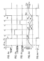
- FIGS. 4a to 4e illustrate a first embodiment of the method of the invention, in which the training charge Q0 is constituted by a pulse of light or driving illumination which is located between the end of a reading pulse IL and the start of signal by signal useful illumination.
- FIG. 4a shows the read pulses IL which bring the voltage VL of the line conductors to a value VL1 positive with respect to the reference voltage VR;
- FIG. 4b makes it possible to locate the drive lighting phase over time;
- FIG. 4c represents the signal illumination pulse;
- FIG. 4d represents the values of the voltage Va at point A;
- FIG. 4e illustrates the open (1) or closed (0) state of the reset switches IL1 to IL3 which it can now be observed that they allow integration, by the amplifiers G1 to G3, of the charges accumulated at the point A during the reading pulses IL1, IL2.
- the instant t1 corresponds, as in the example of FIG. 3, to the falling edge of a read pulse IL1 which has lasted a time TL since the instant t0.
- the establishment of the first reading pulse IL1 at time t0 led the voltage VA to reach, at time t1, a value VA2 lower than the value VL1; and with the falling edge of the first read pulse IL1, the voltage VA decreases to the value VA3 as a result of a voltage variation - ⁇ VC.
- the voltage VA retains the value VA3 until an instant t2 where a drive illumination begins which is applied until an instant t3.
- the voltage VA decreases and goes from the value VA3 to a value VA5, that is to say a variation ⁇ Ve which corresponds to the load QO training previously mentioned.
- the voltage VA retains its value VA5 until an instant t4 where the signal illumination begins, which signal illumination lasts until an instant t5.
- a QS signal charge is generated at point A which causes a variation ⁇ VS of the voltage VA, this variation ⁇ VS being in the direction of a decrease which is added to the variation ⁇ Ve (representing the training load Q0) to lower the voltage VA to the value VA4 for example.
- the value VA4 of the voltage VA is kept until an instant t6 when a second reading pulse IL2 begins.
- the voltage VA shows an increase ⁇ Vc from which it increases and tends towards the value VL1 of the reading pulse IL2; at time t7 which corresponds to the end of the reading pulse IL2, and at the start of a following cycle, the voltage VA has reached a value V FLE, that is to say the value for the end of reading d 'illumination and shows a decrease corresponding to the variation ⁇ Vc.
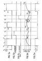
- FIGS. 5a to 5d are diagrams of explanatory signals of the reading method according to the invention, according to a second variant of the latter.
- FIG. 5a are read pulses IL1, IL2 which are applied as before to the first line conductor L1 with an amplitude VL1; and a partial reading pulse ILP having the same polarity as the reading pulses but an amplitude VL2 less than the amplitude VL1 is also applied between two read pulses IL1, IL2.
- FIG. 5b represents the drive illumination;
- FIG. 5c represents the signal illumination;
- FIG. 5d shows the values of the voltage VA at point A;
- FIG. 5e illustrates the open (1) or closed (0) state of the reset switch I1 to I3 and shows that the integration of the charges accumulated at point A by an amplifier G1 to G3 is authorized for the duration a reading pulse IL1, IL2.
- the instant t1 corresponds to the end of a reading phase of the previous cycle, that is to say to the end of a reading pulse IL1 which, from the instant t0 a lasted a time TL.
- the instant t1 therefore marks the falling edge of the first read pulse IL1, and a variation ⁇ Vc of the voltage VA at point A which changes from the value VA2 to the value VA3.
- the instant t1 marks the end of the reading phase of all the photosensitive points of the first line conductor L1.
- the value VA3 of the voltage VA being kept until time t2.
- the training charge Q0 is created, for example for all the photosensitive points of the matrix, by sending a training illumination for the entire detector panel.
- the drive illumination has the effect, at the first photosensitive point P1 for example, of causing a variation ⁇ Ve of the voltage VA such as in the example in FIG. 4, this variation ⁇ Ve leading to a reduction in the voltage VA which goes from the value VA3 to the value VA5.
- the voltage VA retains the value VA5 until an instant t4.
- a partial reading pulse ILP of amplitude VL2 is sent, either simultaneously or successively on all the line conductors L1 to L3.
- This partial reading pulse ILP must have an amplitude VL2 less than the amplitude VL1 of a reading pulse IL1, IL2 and be greater than the voltage VA5, that is to say the voltage which exists at the moment t4 between point A and the reference voltage VR. Under these conditions, the partial reading pulse makes it possible to make a partial reading of the training charge Q0 present at point A, that is to say to eliminate part of this training charge.
- the voltage VA shows an increase ⁇ Vc ′ which depends on the amplitude VL2 and the capacitance ratio Ca, Cb, the first diode Da then being reverse biased; then the voltage VA increases and tends towards the value VL2 until time t5 then shows a decrease - ⁇ Vc by capacitive division which gives it a value Va7.
- the value Va7 of the voltage VA is kept until time t6 when the signal illumination begins which lasts until time t7. Between time t6 and time t7, the voltage VA decreases by a variation ⁇ Vs caused by the accumulation of the quantity of signal charges QS at point A.
- the voltage VA then has a value Va8 which it keeps until the instant t8 which marks the start of the second reading pulse IL2.
- the voltage VA shows a rapid increase ⁇ Vc then increases more slowly to reach an end of reading value of illumination V FLE at an instant T9 which marks the end of the second reading pulse IL2.
- the second reading pulse IL2 made it possible to read the QS signal charge, to which was added a residual training charge Q0 ′ which corresponds to the remaining training charge portion, that is to say not subtracted from point A during partial reading between times t4 and t5 by the partial reading pulse ILP.
- This second variant of the method can be used if the drive illumination has caused the voltage VA to drop, so that the voltage VL2 of the partial reading pulse ILP is greater than this voltage VA by an amount at least equal to the value of its direct elbow tension.
- the implementation of the method of the invention is all the more advantageous since the second diode Db has in reverse a large capacitance Cb with respect to the capacitance Ca that in reverse has the first diode Da.
- a photodiode having a higher inverse capacity generates a greater amount of charge: so that when a photosensitive point P1 to P9 is illuminated, most of the charges are generated by the second diode Db, what lends itself particularly good at producing a training charge Q0 generated by a training illumination; the first diode Da possibly being "blind".
Landscapes
- Engineering & Computer Science (AREA)
- Multimedia (AREA)
- Signal Processing (AREA)
- Transforming Light Signals Into Electric Signals (AREA)
Applications Claiming Priority (2)
| Application Number | Priority Date | Filing Date | Title |
|---|---|---|---|
| FR8812126A FR2636800A1 (fr) | 1988-09-16 | 1988-09-16 | Procede de lecture de cellules photosensibles du type comportant deux diodes montees en serie avec des sens de conduction opposes |
| FR8812126 | 1988-09-16 |
Publications (2)
| Publication Number | Publication Date |
|---|---|
| EP0364314A1 true EP0364314A1 (de) | 1990-04-18 |
| EP0364314B1 EP0364314B1 (de) | 1994-03-30 |
Family
ID=9370082
Family Applications (1)
| Application Number | Title | Priority Date | Filing Date |
|---|---|---|---|
| EP89402483A Expired - Lifetime EP0364314B1 (de) | 1988-09-16 | 1989-09-12 | Verfahren zum Lesen von lichtempfindlichen Zellen mit zwei in Reihe angeordneten Dioden und mit entgegenwirkenden Durchlassrichtungen |
Country Status (4)
| Country | Link |
|---|---|
| US (1) | US4948966A (de) |
| EP (1) | EP0364314B1 (de) |
| DE (1) | DE68914239T2 (de) |
| FR (1) | FR2636800A1 (de) |
Cited By (7)
| Publication number | Priority date | Publication date | Assignee | Title |
|---|---|---|---|---|
| EP0670656A3 (de) * | 1994-03-03 | 1996-02-28 | Philips Electronics Uk Ltd | Bildaufnahmevorrichtung. |
| FR2760585A1 (fr) * | 1997-03-07 | 1998-09-11 | Thomson Tubes Electroniques | Procede de commande d'un dispositif photosensible a faible remanence, et dispositif photosensible mettant en oeuvre le procede |
| FR2770954A1 (fr) * | 1997-11-12 | 1999-05-14 | Trixell Sas | Procede de commande d'un detecteur d'image numerique a faible remanence, et detecteur d'image mettant en oeuvre le procede |
| FR2771513A1 (fr) * | 1997-11-25 | 1999-05-28 | Trixell Sas | Dispositif photosensible equipe d'un dispositif de mesure d'eclairement |
| WO2001003419A1 (fr) * | 1999-07-06 | 2001-01-11 | Trixell S.A.S. | Procede de commande d'un dispositif photosensible apte a produire des images de bonne qualite |
| JP2003529972A (ja) * | 1999-12-28 | 2003-10-07 | トリクセル エス.アー.エス. | 画像検出器の温度補償方法 |
| EP3026890A1 (de) * | 2014-11-24 | 2016-06-01 | Commissariat A L'energie Atomique Et Aux Energies Alternatives | Steuerung der integrationszeit in einem lichtempfindlichen apparat |
Families Citing this family (18)
| Publication number | Priority date | Publication date | Assignee | Title |
|---|---|---|---|---|
| DE3940164A1 (de) * | 1989-12-05 | 1991-06-06 | Philips Patentverwaltung | Anordnung zum auslesen licht- oder roentgenstrahlenempfindlicher sensoren |
| JP2601933B2 (ja) * | 1990-04-13 | 1997-04-23 | 株式会社東芝 | 固体撮像装置 |
| US5324958A (en) * | 1991-02-19 | 1994-06-28 | Synaptics, Incorporated | Integrating imaging systgem having wide dynamic range with sample/hold circuits |
| US5097305A (en) * | 1991-02-19 | 1992-03-17 | Synaptics Corporation | Integrating photosensor and imaging system having wide dynamic range |
| US5260592A (en) * | 1991-02-19 | 1993-11-09 | Synaptics, Incorporated | Integrating photosensor and imaging system having wide dynamic range with varactors |
| US5502488A (en) * | 1991-05-07 | 1996-03-26 | Olympus Optical Co., Ltd. | Solid-state imaging device having a low impedance structure |
| JP2838735B2 (ja) * | 1991-07-05 | 1998-12-16 | 富士ゼロックス株式会社 | 画像読取装置 |
| DE4321789C2 (de) * | 1993-06-30 | 1999-12-09 | Siemens Ag | Festkörperbildwandler |
| GB9404111D0 (en) * | 1994-03-03 | 1994-04-20 | Philips Electronics Uk Ltd | A charge storage device |
| GB9404113D0 (en) * | 1994-03-03 | 1994-04-20 | Philips Electronics Uk Ltd | A charge storage device |
| FR2731569B1 (fr) * | 1995-03-07 | 1997-04-25 | Thomson Tubes Electroniques | Dispositif de recopie de tension a grande linearite |
| GB9505305D0 (en) * | 1995-03-16 | 1995-05-03 | Philips Electronics Uk Ltd | Electronic devices comprising an array |
| DE19606873C2 (de) * | 1996-02-23 | 2000-10-12 | Siemens Ag | Röntgendiagnostikeinrichtung mit einem Festkörperbildwandler |
| FR2758656B1 (fr) | 1997-01-21 | 1999-04-09 | Thomson Tubes Electroniques | Procede de realisation d'un detecteur de rayonnement par assemblage de dalles elementaires et detecteur ainsi obtenu |
| FR2762741A1 (fr) * | 1997-04-25 | 1998-10-30 | Thomson Tubes Electroniques | Procede de commande d'un detecteur d'image offrant une protection contre les eblouissements, et detecteur d'image mettant en oeuvre le procede |
| US6759641B1 (en) * | 2000-09-27 | 2004-07-06 | Rockwell Scientific Licensing, Llc | Imager with adjustable resolution |
| FR2818073B1 (fr) * | 2000-12-07 | 2003-01-10 | Commissariat Energie Atomique | Circuit de lecture de charges par calibration et procede de lecture de charges par calibration |
| KR100602066B1 (ko) * | 2003-09-30 | 2006-07-14 | 엘지전자 주식회사 | 일렉트로 루미네센스 표시소자의 구동방법 및 장치 |
Citations (2)
| Publication number | Priority date | Publication date | Assignee | Title |
|---|---|---|---|---|
| EP0245147A1 (de) * | 1986-04-30 | 1987-11-11 | Thomson-Csf | Röntgen-Bilderfassungstafel und deren Herstellungsverfahren |
| FR2605166A1 (fr) * | 1986-10-09 | 1988-04-15 | Thomson Csf | Dispositif photosensible a l'etat solide, procede de lecture et procede de fabrication |
Family Cites Families (3)
| Publication number | Priority date | Publication date | Assignee | Title |
|---|---|---|---|---|
| JPS575371A (en) * | 1980-06-11 | 1982-01-12 | Ricoh Co Ltd | Image sensor |
| US4826777A (en) * | 1987-04-17 | 1989-05-02 | The Standard Oil Company | Making a photoresponsive array |
| US4785191A (en) * | 1987-04-17 | 1988-11-15 | Stemcor Corporation | Interconnected array of photosensors for simultaneously sensing light intensities at each of a number of locations |
-
1988
- 1988-09-16 FR FR8812126A patent/FR2636800A1/fr not_active Withdrawn
-
1989
- 1989-09-12 DE DE68914239T patent/DE68914239T2/de not_active Expired - Lifetime
- 1989-09-12 EP EP89402483A patent/EP0364314B1/de not_active Expired - Lifetime
- 1989-09-12 US US07/406,150 patent/US4948966A/en not_active Expired - Lifetime
Patent Citations (2)
| Publication number | Priority date | Publication date | Assignee | Title |
|---|---|---|---|---|
| EP0245147A1 (de) * | 1986-04-30 | 1987-11-11 | Thomson-Csf | Röntgen-Bilderfassungstafel und deren Herstellungsverfahren |
| FR2605166A1 (fr) * | 1986-10-09 | 1988-04-15 | Thomson Csf | Dispositif photosensible a l'etat solide, procede de lecture et procede de fabrication |
Cited By (12)
| Publication number | Priority date | Publication date | Assignee | Title |
|---|---|---|---|---|
| EP0670656A3 (de) * | 1994-03-03 | 1996-02-28 | Philips Electronics Uk Ltd | Bildaufnahmevorrichtung. |
| FR2760585A1 (fr) * | 1997-03-07 | 1998-09-11 | Thomson Tubes Electroniques | Procede de commande d'un dispositif photosensible a faible remanence, et dispositif photosensible mettant en oeuvre le procede |
| WO1998041010A1 (fr) * | 1997-03-07 | 1998-09-17 | Thomson Tubes Electroniques | Procede de commande d'un dispositif photosensible a faible remanence, et dispositif photosensible mettant en oeuvre le procede |
| FR2770954A1 (fr) * | 1997-11-12 | 1999-05-14 | Trixell Sas | Procede de commande d'un detecteur d'image numerique a faible remanence, et detecteur d'image mettant en oeuvre le procede |
| FR2771513A1 (fr) * | 1997-11-25 | 1999-05-28 | Trixell Sas | Dispositif photosensible equipe d'un dispositif de mesure d'eclairement |
| US6410898B1 (en) | 1997-11-25 | 2002-06-25 | Trixell S.A.S. | Photosensitive device equipped with an illumination measurement device |
| WO2001003419A1 (fr) * | 1999-07-06 | 2001-01-11 | Trixell S.A.S. | Procede de commande d'un dispositif photosensible apte a produire des images de bonne qualite |
| FR2796239A1 (fr) * | 1999-07-06 | 2001-01-12 | Trixell Sas | Procede de commande d'un dispositif photosensible apte a produire des images de bonne qualite |
| US6980246B1 (en) | 1999-07-06 | 2005-12-27 | Trixell S.A.S. | Process for controlling a photosensitive device including a photosensitive point produced by techniques for depositing semiconductor materials |
| JP2003529972A (ja) * | 1999-12-28 | 2003-10-07 | トリクセル エス.アー.エス. | 画像検出器の温度補償方法 |
| EP3026890A1 (de) * | 2014-11-24 | 2016-06-01 | Commissariat A L'energie Atomique Et Aux Energies Alternatives | Steuerung der integrationszeit in einem lichtempfindlichen apparat |
| US9686491B2 (en) | 2014-11-24 | 2017-06-20 | Commissariat A L'energie Atomique Et Aux Energies Alternatives | Device and method to control a duration of integration in a photosensitive device having a matrix of photosensitive pixels |
Also Published As
| Publication number | Publication date |
|---|---|
| EP0364314B1 (de) | 1994-03-30 |
| FR2636800A1 (fr) | 1990-03-23 |
| US4948966A (en) | 1990-08-14 |
| DE68914239T2 (de) | 1994-08-11 |
| DE68914239D1 (de) | 1994-05-05 |
Similar Documents
| Publication | Publication Date | Title |
|---|---|---|
| EP0364314B1 (de) | Verfahren zum Lesen von lichtempfindlichen Zellen mit zwei in Reihe angeordneten Dioden und mit entgegenwirkenden Durchlassrichtungen | |
| EP0237365B1 (de) | Lichtempfindliche Vorrichtung | |
| EP0367650B1 (de) | Photoempfindliche Vorrichtung mit Signalverstärkung im Bereich der photoempfindlichen Punkte | |
| EP0028960B1 (de) | Strahlungsdetektorenmatrix und Röntgenbild-Verstärker mit einer solchen Matrix | |
| EP0245147A1 (de) | Röntgen-Bilderfassungstafel und deren Herstellungsverfahren | |
| EP0233104A1 (de) | Matrix photoempfindlicher Elemente und deren Herstellungsverfahren, zugehöriges Ausleseverfahren und Anwendung dieser Matrix bei der Bildaufnahme | |
| EP0332486A1 (de) | Matrix photoempfindlicher Elemente und Strahlungssensor mit einer solchen Matrix, insbesondere Doppel-Energie-Röntgensensor | |
| EP0331546B1 (de) | Photoempfindlicher Matrix mit zwei Dioden pro Punkt ohne spezifischen Rückstellungsleiter | |
| EP0324677B1 (de) | Photoempfindliche Matrix mit drei Dioden pro Punkt ohne Rückstellung | |
| EP0965224B1 (de) | Verfahren zur steuerung einer lichtempfindlichen vorrichtung mit schwacher remanenz und lichtempfindliche vorrichtung zur durchführung des verfahrens | |
| EP0234968A1 (de) | Leseverfahren eines photoempfindlichen Elements, bestehend aus einer Photodiode und einer Kapazität | |
| FR2549328A1 (fr) | Dispositif photosensible a l'etat solide | |
| EP1673932B1 (de) | Steuerverfahren für eine lichtempfindliche einrichtung | |
| EP0357468B1 (de) | Photoempfindliche Matrix mit zwei Dioden gleicher Polarität und einer Kapazität pro photoempfindlichem Punkt | |
| EP1796373A1 (de) | Abbildungsverfahren mit Hilfe eines Bildsensors mit grossem dynamik Bereich | |
| EP0236157B1 (de) | Schnelle Abtastvorrichtung für einen optischen in einer Matrixform angeordneten Ladungsübertragungssensor bei einer Halbbildübertragung für die Detektion von kurzen Videobildern | |
| EP1195049B1 (de) | Steuerungsverfahren für eine lichtempfindliche vorrichtung fähig zur erzeugeug von bildern mit guter qualität | |
| CA2449939C (fr) | Procede de commande d'un dispositif photosensible | |
| FR2568709A1 (fr) | Circuit matriciel | |
| EP0324678A1 (de) | Photoempfindliche Matrix mit zwei Dioden und einer Kapazität pro Punkt ohne optische Rückstellung | |
| FR2770954A1 (fr) | Procede de commande d'un detecteur d'image numerique a faible remanence, et detecteur d'image mettant en oeuvre le procede | |
| FR2762741A1 (fr) | Procede de commande d'un detecteur d'image offrant une protection contre les eblouissements, et detecteur d'image mettant en oeuvre le procede | |
| FR3084553A1 (fr) | Capteur optique | |
| EP0818827A1 (de) | Fotodetektor mit verbesserter Reaktionszeit und Sensormatrix mit einer Vielzahl von Fotodetektoren | |
| EP0217691A1 (de) | Abtastung und Halteschaltung mit Diodenbrücke |
Legal Events
| Date | Code | Title | Description |
|---|---|---|---|
| PUAI | Public reference made under article 153(3) epc to a published international application that has entered the european phase |
Free format text: ORIGINAL CODE: 0009012 |
|
| AK | Designated contracting states |
Kind code of ref document: A1 Designated state(s): DE FR GB NL |
|
| 17P | Request for examination filed |
Effective date: 19900504 |
|
| 17Q | First examination report despatched |
Effective date: 19920721 |
|
| GRAA | (expected) grant |
Free format text: ORIGINAL CODE: 0009210 |
|
| RAP1 | Party data changed (applicant data changed or rights of an application transferred) |
Owner name: THOMSON-CSF |
|
| AK | Designated contracting states |
Kind code of ref document: B1 Designated state(s): DE FR GB NL |
|
| PG25 | Lapsed in a contracting state [announced via postgrant information from national office to epo] |
Ref country code: GB Effective date: 19940330 |
|
| REF | Corresponds to: |
Ref document number: 68914239 Country of ref document: DE Date of ref document: 19940505 |
|
| GBV | Gb: ep patent (uk) treated as always having been void in accordance with gb section 77(7)/1977 [no translation filed] |
Effective date: 19940330 |
|
| PLBE | No opposition filed within time limit |
Free format text: ORIGINAL CODE: 0009261 |
|
| STAA | Information on the status of an ep patent application or granted ep patent |
Free format text: STATUS: NO OPPOSITION FILED WITHIN TIME LIMIT |
|
| 26N | No opposition filed | ||
| PGFP | Annual fee paid to national office [announced via postgrant information from national office to epo] |
Ref country code: NL Payment date: 20080903 Year of fee payment: 20 Ref country code: FR Payment date: 20080915 Year of fee payment: 20 |
|
| PGFP | Annual fee paid to national office [announced via postgrant information from national office to epo] |
Ref country code: DE Payment date: 20080926 Year of fee payment: 20 |
|
| NLV7 | Nl: ceased due to reaching the maximum lifetime of a patent |
Effective date: 20090912 |
|
| PG25 | Lapsed in a contracting state [announced via postgrant information from national office to epo] |
Ref country code: NL Free format text: LAPSE BECAUSE OF EXPIRATION OF PROTECTION Effective date: 20090912 |