EP0364700A2 - Circuit de couplage à un bus - Google Patents
Circuit de couplage à un bus Download PDFInfo
- Publication number
- EP0364700A2 EP0364700A2 EP89115672A EP89115672A EP0364700A2 EP 0364700 A2 EP0364700 A2 EP 0364700A2 EP 89115672 A EP89115672 A EP 89115672A EP 89115672 A EP89115672 A EP 89115672A EP 0364700 A2 EP0364700 A2 EP 0364700A2
- Authority
- EP
- European Patent Office
- Prior art keywords
- bus
- driver
- voltage
- hysteresis
- arrangement according
- Prior art date
- Legal status (The legal status is an assumption and is not a legal conclusion. Google has not performed a legal analysis and makes no representation as to the accuracy of the status listed.)
- Granted
Links
- 238000010168 coupling process Methods 0.000 title claims abstract description 16
- 238000005859 coupling reaction Methods 0.000 title claims abstract description 16
- 230000008878 coupling Effects 0.000 claims abstract description 15
- 230000002457 bidirectional effect Effects 0.000 claims abstract description 10
- 239000003990 capacitor Substances 0.000 claims description 27
- 238000002955 isolation Methods 0.000 claims description 10
- 230000005540 biological transmission Effects 0.000 claims description 5
- 230000000903 blocking effect Effects 0.000 abstract 1
- 230000000694 effects Effects 0.000 description 4
- 238000004804 winding Methods 0.000 description 4
- 230000008901 benefit Effects 0.000 description 3
- 238000005516 engineering process Methods 0.000 description 3
- 238000000034 method Methods 0.000 description 3
- 230000008569 process Effects 0.000 description 3
- 238000004364 calculation method Methods 0.000 description 2
- 230000001419 dependent effect Effects 0.000 description 2
- 229910000859 α-Fe Inorganic materials 0.000 description 2
- XUIMIQQOPSSXEZ-UHFFFAOYSA-N Silicon Chemical compound [Si] XUIMIQQOPSSXEZ-UHFFFAOYSA-N 0.000 description 1
- 238000004458 analytical method Methods 0.000 description 1
- 238000005266 casting Methods 0.000 description 1
- 230000015556 catabolic process Effects 0.000 description 1
- 230000003749 cleanliness Effects 0.000 description 1
- 238000010276 construction Methods 0.000 description 1
- 238000013016 damping Methods 0.000 description 1
- 230000002950 deficient Effects 0.000 description 1
- 238000011161 development Methods 0.000 description 1
- 230000018109 developmental process Effects 0.000 description 1
- 230000003071 parasitic effect Effects 0.000 description 1
- 230000001681 protective effect Effects 0.000 description 1
- 230000009467 reduction Effects 0.000 description 1
- 230000035945 sensitivity Effects 0.000 description 1
- 229910052710 silicon Inorganic materials 0.000 description 1
- 239000010703 silicon Substances 0.000 description 1
- 230000006641 stabilisation Effects 0.000 description 1
- 238000011105 stabilization Methods 0.000 description 1
- 230000003068 static effect Effects 0.000 description 1
Images


Classifications
-
- H—ELECTRICITY
- H04—ELECTRIC COMMUNICATION TECHNIQUE
- H04L—TRANSMISSION OF DIGITAL INFORMATION, e.g. TELEGRAPHIC COMMUNICATION
- H04L12/00—Data switching networks
- H04L12/28—Data switching networks characterised by path configuration, e.g. LAN [Local Area Networks] or WAN [Wide Area Networks]
- H04L12/40—Bus networks
- H04L12/40006—Architecture of a communication node
- H04L12/40032—Details regarding a bus interface enhancer
-
- H—ELECTRICITY
- H04—ELECTRIC COMMUNICATION TECHNIQUE
- H04L—TRANSMISSION OF DIGITAL INFORMATION, e.g. TELEGRAPHIC COMMUNICATION
- H04L12/00—Data switching networks
- H04L12/02—Details
- H04L12/10—Current supply arrangements
Definitions
- the invention relates to a bus coupling circuit based on the preamble of patent claim 1.
- Such a bus coupling circuit is known from "Control engineering practice, 25th year, 1983, number 10, pages S61 to S64, and number 10, pages S69 and S70".
- a bus receiver has a hysteresis for suppressing superimposed interference signals.
- Participants e.g. Data transmitters or data receivers, which are connected to one another via a common bus, have driver circuits as interfaces. In the event of a short-circuit in a subscriber or in an interface, the entire bus is often unusable.
- an interface arrangement constructed with optocouplers is known which, in the event of faults in the optocouplers, e.g. in the event of short circuits, a control circuit assigned to the optocouplers prevents the connection between driver and data input from being blocked.
- the object of the invention is to design the bus coupling circuit according to the preamble of patent claim 1 such that bidirectional operation with high data rates is possible even when component failures, in particular short circuits, occur.
- the DC voltage value lost due to the galvanic isolation is restored without distortion by an additional hysteresis circuit. This allows operation with high data rates, since only edges of the data signal have to be evaluated.
- a component in the hysteresis circuit is dimensioned so that bidirectional bus operation is still possible even in the event of short circuits.
- the arrangement according to the invention allows bidirectional data transmission with electrical fault tolerance of several, for example eight, short circuits. Other errors, such as participants marked by mere failure, are negligible for the bus.
- the bus system does not require any clock lines for "bus handling", which further increases reliability. It is also insensitive to incorrect control, since the series resistors, as components of the DC isolating means, also act as protective impedances. An accidentally "clamped” on the bus Driver output (transmission mode) has the same non-disadvantageous effect on the bus as the short circuit of a driver output since static signals are not present on the bus and the DC value is recovered from the edges of the data by artificial hysteresis.
- the configurations according to patent claims 4, 5 and 7 and patent claim 10 have the following additional advantages:
- the signal shape of the digital signals transmitted by the bus improves especially at bit rates> 20 Mbit / s without significantly narrowing the fault tolerance. If the boundary conditions are otherwise the same, more short circuits can be permitted than with the arrangement according to the main application.
- the measures of the invention give the bus an amplitude-dependent passive dynamic termination or an active bus termination (claim 10).
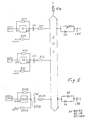
- the bus shown in the figure can be connected via a total of 28 bidirectional drivers T1, T2, ... to the subscribers Tl1, Tl2 ..., eg microprocessors.
- the AC 245 integrated circuits of FACT (Fairchild Advanced CMOS Technology) technology are suitable as bidirectional drivers. Two drivers, one representing a data transmitter and the other a data receiver or vice versa, can be switched in real time in a fault-tolerant manner in groups (8 bits) via these drivers. A short circuit or an interruption in a participant must not have any serious effects on the overall system.
- the driver inputs E21, E22 ... close to the bus are connected to the bus via DC voltage isolating means, each consisting of a series connection of a capacitor C1, C2, ...
- the divider chain ie the series connection of the voltage divider resistors, lies between the input E11 or E12, ... of the driver remote from the bus and half the supply voltage - + 2.5 V for the integrated drivers used.
- the threshold reference voltage of the drivers is thus newly available (dashed line in FIG. 1).
- the divider tap is connected to the driver input E21 or E22, ... near the bus.
- a bus earth resistance R4 of approximately 100 KOhm is provided.
- the hysteresis determines the sensitivity of the receiver around the threshold (at FACT 2.5 volts). It specifies the minimum amplitude (reduction due to short circuits) the system stops functioning, or: how many short circuits the system can ultimately cope with. This situation is explained on the basis of the "steady state": If, for example, a positive edge has occurred on the bus, the AC245 is consequently driven to HIGH via resistor R11 or R12 and capacitor C1 or C2 . It is now connected to the bus with the input side.
- a short circuit for example of a driver output, results in a loss of amplitude.
- VCC positive supply potential
- a short circuit of just one driver to GND is assumed: Then the potential would be set to zero without additional measures.
- the dynamic amplitude would be halved (by the resistance of both the transmitter and the receiver), but limited in its maximum value to + 2.5 volts. But that is exactly the threshold, so that no defined state "HIGH" could be transmitted.
- the basic idea now is to remove this distortion of the DC voltage value by taking additional measures. For this purpose, a sufficiently large capacitor C1 or C2, ...
- resistors R2 and R3 have been assumed to be substantially larger than the series resistors in their entire parallel connection along the bus line.
- the current consumption of the bus drivers used is almost exclusively determined by the external wiring.
- the interface arrangement presented is ideally suited for use in MOBS (modular onboard switching) systems in satellites, especially since faults in resistors are almost always only manifested by an interruption and even short circuits in the series capacitors only have a negative effect if the associated driver is also involved fails due to short circuit. However, this case occurs with a very low probability of association.
- the DC voltage isolation can also be carried out differently than previously described, for example by a transformer U1, U2, ... (FIG. 2). Its secondary winding w2 can be connected directly to the bus, for example.
- the primary winding w1 (of the transformer U1) is connected with its one connection end to the driver input E21 and with its other connection end to the divider tap of the voltage divider consisting of the resistors R21, R31, or R22, R32.
- the voltage divider resistors For the dimensioning of the voltage divider resistors, it must be assumed that on the one hand they must be so high-resistance that the short circuit of a driver is not transformed to the bus as a short circuit or too low impedance, but on the other hand it must also be so low-resistance that a driver has enough power in the direction of transmission can transform to the bus in order to control all other drivers operated as receivers via their assigned transmitters. In real cases, not all of the driver power is transferred to the bus due to leakage losses from the transformers. These requirements are met if the AC parallel impedance of the resistors R2 and R3 is in the order of 100 ohms.
- a high-frequency ferrite core transformer is preferably suitable as the transformer Ü.
- the implementation by means of a transformer as a DC voltage isolation means requires fewer components than the solution presented above with a DC voltage isolation capacitor.
- the probability of failure of the high-frequency ferrite core transformers can be reduced by special construction measures (casting, winding arrangement with a large winding spacing).
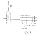
- the bus is "open" for signal amplitudes on the bus less than 0.7 V; ie only the ohmic bus ground resistance R4 is effective. If the signal amplitudes on the bus rise above U S , the excess amplitude components are cut off at ⁇ 0.7 V. If a short circuit now occurs, for example at a bus driver output, the bus is additionally loaded in terms of AC voltage with the corresponding resistor R11 ... R128, at whose driver the short circuit occurs. This reduces the signal amplitudes on the bus. The corresponding resistor R11 ... R128 then takes over the bus termination.
- the signal amplitudes on the bus which were previously sufficient to control the diodes D1, D2, D3 and D4, can drop to such an extent that the threshold value U S no longer reaches due to the load with one of the resistors R11 ... becomes.
- the threshold value U S is reached despite additional loading by one of the resistors R11 ... R128, and what is known as a voltage divider behavior occurs:
- the bus is then terminated both with the corresponding resistor R11 ... R128 and with the path resistance of the diodes D1, D2, D3 and D4.
- the resistor R4 is several orders of magnitude larger than the resistors R11 ...
- capacitors CB1 and CB2 must be chosen so large in terms of capacity that the DC voltage value for the hysteresis circuits can still be regenerated from the edges of the transferable data. It is best to choose capacitors CB1 and CB2 each as large as capacitors C1 to C28.
- FIG. 4 Such an exemplary embodiment for a one-sided bus termination is shown in FIG. 4. Here two series parallel connections of diodes are arranged antiparallel to each other.
- the corresponding DC isolating capacitor consists of four partial capacitors - two capacitors connected in series, which are combined to form a parallel connection.
- care must be taken to ensure that the corresponding threshold value U S and the total capacitance CB1 and CB2 are matched to the bus and the other components.
Landscapes
- Engineering & Computer Science (AREA)
- Computer Networks & Wireless Communication (AREA)
- Signal Processing (AREA)
- Dc Digital Transmission (AREA)
- Small-Scale Networks (AREA)
- Heterocyclic Carbon Compounds Containing A Hetero Ring Having Oxygen Or Sulfur (AREA)
Applications Claiming Priority (4)
| Application Number | Priority Date | Filing Date | Title |
|---|---|---|---|
| DE3835458 | 1988-10-18 | ||
| DE19883835458 DE3835458A1 (de) | 1988-10-18 | 1988-10-18 | Schnittstellenanordnung fuer ein bussystem |
| DE3905109 | 1989-02-20 | ||
| DE3905109 | 1989-02-20 |
Publications (3)
| Publication Number | Publication Date |
|---|---|
| EP0364700A2 true EP0364700A2 (fr) | 1990-04-25 |
| EP0364700A3 EP0364700A3 (fr) | 1992-07-22 |
| EP0364700B1 EP0364700B1 (fr) | 1995-05-03 |
Family
ID=25873355
Family Applications (1)
| Application Number | Title | Priority Date | Filing Date |
|---|---|---|---|
| EP89115672A Expired - Lifetime EP0364700B1 (fr) | 1988-10-18 | 1989-08-25 | Circuit de couplage à un bus |
Country Status (4)
| Country | Link |
|---|---|
| US (1) | US4985903A (fr) |
| EP (1) | EP0364700B1 (fr) |
| CA (2) | CA1337826C (fr) |
| DE (1) | DE58909214D1 (fr) |
Cited By (4)
| Publication number | Priority date | Publication date | Assignee | Title |
|---|---|---|---|---|
| EP0427921A3 (en) * | 1989-11-14 | 1994-07-27 | Ant Nachrichtentech | Method and device for data transmission |
| WO2000076159A1 (fr) * | 1999-06-07 | 2000-12-14 | Siemens Audiologische Technik Gmbh | Interface pour la separation de potentiel et pour la transmission de signaux numeriques |
| WO2001047111A3 (fr) * | 1999-12-21 | 2002-02-14 | Teradyne Inc | Circuit de rereferencement couple en mode capacitif avec retroaction positive |
| EP3884626A1 (fr) * | 2018-11-22 | 2021-09-29 | Robert Bosch GmbH | Dispositif d'affaiblissement de réflexions pour un bus d'un système de bus et procédé d'affaiblissement de réflexions lors d'une transmission de données dans un système de bus |
Families Citing this family (8)
| Publication number | Priority date | Publication date | Assignee | Title |
|---|---|---|---|---|
| US5134311A (en) * | 1990-06-07 | 1992-07-28 | International Business Machines Corporation | Self-adjusting impedance matching driver |
| DE59303775D1 (de) * | 1992-06-02 | 1996-10-17 | Siemens Ag | Teilnehmerstation der gebäudesystemtechnik |
| KR950012306B1 (ko) * | 1993-03-25 | 1995-10-16 | 삼성전자주식회사 | 디지탈 정보전달 버스구조 및 디지탈 정보전달방법 |
| JP2882266B2 (ja) * | 1993-12-28 | 1999-04-12 | 株式会社日立製作所 | 信号伝送装置及び回路ブロック |
| US5561694A (en) * | 1995-07-26 | 1996-10-01 | International Business Machines Corporation | Self-timed driver circuit |
| IT1278522B1 (it) | 1995-11-27 | 1997-11-24 | Italtel Spa | Metodo e dispositivo per correggere gli errori di trasmissione ed individuare le unita' guaste nell'ambito di una trasmissione di dati |
| US6219812B1 (en) * | 1998-06-11 | 2001-04-17 | Sun Microsystems, Inc. | Apparatus and method for interfacing boundary-scan circuitry with DTL output drivers |
| CN105843195B (zh) * | 2016-05-24 | 2019-02-01 | 中国科学院长春光学精密机械与物理研究所 | 多控制器的上电控制系统 |
Family Cites Families (8)
| Publication number | Priority date | Publication date | Assignee | Title |
|---|---|---|---|---|
| GB1200486A (en) * | 1967-04-18 | 1970-07-29 | Int Computers Ltd | Data transmitting apparatus |
| US3875332A (en) * | 1973-12-27 | 1975-04-01 | Nasa | Digital transmitter for data bus communications system |
| DK143627C (da) * | 1978-10-30 | 1982-02-15 | Rovsing A S | Koblingskreds til overfoering af datasignaler med stor hastighed |
| FR2443770A1 (fr) * | 1978-12-04 | 1980-07-04 | Materiel Telephonique | Recepteur pour bus ac a isolation galvanique par capacite |
| FR2452207A1 (fr) * | 1979-03-20 | 1980-10-17 | Matra | Perfectionnements aux dispositifs de couplage d'emetteur sur voie commune et installation de transmission en comportant application |
| US4614882A (en) * | 1983-11-22 | 1986-09-30 | Digital Equipment Corporation | Bus transceiver including compensation circuit for variations in electrical characteristics of components |
| DE3433150A1 (de) * | 1984-09-10 | 1986-03-20 | Siemens AG, 1000 Berlin und 8000 München | Schnittstellenanordnung zur ankopplung einer teilnehmerschaltung an eine datenuebertragungsleitung |
| EP0184816A3 (fr) * | 1984-12-13 | 1989-01-11 | Honeywell Inc. | Système de transmission de données |
-
1989
- 1989-08-25 EP EP89115672A patent/EP0364700B1/fr not_active Expired - Lifetime
- 1989-08-25 DE DE58909214T patent/DE58909214D1/de not_active Expired - Fee Related
- 1989-09-29 CA CA000615005A patent/CA1337826C/fr not_active Expired - Fee Related
- 1989-10-17 US US07/422,516 patent/US4985903A/en not_active Expired - Fee Related
- 1989-10-18 CA CA002000919A patent/CA2000919A1/fr not_active Abandoned
Cited By (5)
| Publication number | Priority date | Publication date | Assignee | Title |
|---|---|---|---|---|
| EP0427921A3 (en) * | 1989-11-14 | 1994-07-27 | Ant Nachrichtentech | Method and device for data transmission |
| WO2000076159A1 (fr) * | 1999-06-07 | 2000-12-14 | Siemens Audiologische Technik Gmbh | Interface pour la separation de potentiel et pour la transmission de signaux numeriques |
| WO2001047111A3 (fr) * | 1999-12-21 | 2002-02-14 | Teradyne Inc | Circuit de rereferencement couple en mode capacitif avec retroaction positive |
| EP3884626A1 (fr) * | 2018-11-22 | 2021-09-29 | Robert Bosch GmbH | Dispositif d'affaiblissement de réflexions pour un bus d'un système de bus et procédé d'affaiblissement de réflexions lors d'une transmission de données dans un système de bus |
| US11750176B2 (en) | 2018-11-22 | 2023-09-05 | Robert Bosch Gmbh | Reflection attenuation device for a bus of a bus system, and method for attenuating reflections during a data transfer in a bus system |
Also Published As
| Publication number | Publication date |
|---|---|
| EP0364700B1 (fr) | 1995-05-03 |
| US4985903A (en) | 1991-01-15 |
| CA2000919A1 (fr) | 1990-04-18 |
| CA1337826C (fr) | 1995-12-26 |
| EP0364700A3 (fr) | 1992-07-22 |
| DE58909214D1 (de) | 1995-06-08 |
Similar Documents
| Publication | Publication Date | Title |
|---|---|---|
| EP0090255B1 (fr) | Circuit de commande à trois états | |
| DE60005365T2 (de) | Elektrische isolierungsvorrichtung mit optokoppler für bidirektionelle anschlussleitungen | |
| EP0364700B1 (fr) | Circuit de couplage à un bus | |
| DE102015118514A1 (de) | Signalisolatorsystem mit Schutz für Gleichtakttransienten | |
| EP0855758A1 (fr) | Circuit pour protection de circuits d'entrée HF de dispositifs de télécommunication | |
| EP0500557A1 (fr) | Circuit multiplex, notamment pour commander des postes consommateurs dans des vehicules a moteur. | |
| DE3311881C2 (fr) | ||
| EP1568149A1 (fr) | Circuit de protection contre la surtension pour un emetteur-recepteur de bus can | |
| EP2110950B1 (fr) | Circuit et procédé de transmission de tension de signal à l'intérieur d'un pilote d'un circuit semi-conducteur de puissance | |
| WO2006072292A1 (fr) | Ensemble circuit et procede pour proteger un circuit par rapport a des decharges electrostatiques | |
| EP0427921B1 (fr) | Méthode et dispositif de transmission de données | |
| DE102010042156A1 (de) | Übertragungsvorrichtung für eine differentielle Kommunikation | |
| DE2250859C2 (de) | Schaltungsanordnung für den Übergang von Zwei- auf Vierdrahtbetrieb für Fernmelde-, insbesondere Fernsprechvermittlungsanlagen | |
| DE3835458C2 (fr) | ||
| DE4327035A1 (de) | Anordnung zur bidirektionalen Datenübertragung | |
| DE10305361B4 (de) | Elektronischer Hochfrequenz-Schalter | |
| WO1990008437A2 (fr) | Raccordement de postes a des bus | |
| EP0689291B1 (fr) | Circuit d'attaque du type MOS | |
| DE69903161T2 (de) | Schnittstellenmodul mit schutzkreis und verfahren um eine schnittstelle zu schützen | |
| DE69601198T2 (de) | Kurzschlussschutz für einen Audio-Video-Datenbus | |
| DE102011053904A1 (de) | Schaltungsanordnung zum Schutz von Transceivern von Schnittstellen für drahtgebundene Kommunikation | |
| DE10314514A1 (de) | Leistungsvorrichtungssteuerschaltung | |
| EP3672009B1 (fr) | Circuit de protection, dispositif électronique et procédé de fonctionnement d'un dispositif électronique | |
| DE19925909A1 (de) | Schnittstelle zur Potentialtrennung und zur Übertragung digitaler Signale | |
| DE10133441C2 (de) | Schaltungsanordnung zur Spannungssymmetrierung von Datenbussen |
Legal Events
| Date | Code | Title | Description |
|---|---|---|---|
| PUAI | Public reference made under article 153(3) epc to a published international application that has entered the european phase |
Free format text: ORIGINAL CODE: 0009012 |
|
| AK | Designated contracting states |
Kind code of ref document: A2 Designated state(s): DE FR GB IT NL |
|
| 17P | Request for examination filed |
Effective date: 19901227 |
|
| PUAL | Search report despatched |
Free format text: ORIGINAL CODE: 0009013 |
|
| AK | Designated contracting states |
Kind code of ref document: A3 Designated state(s): DE FR GB IT NL |
|
| 17Q | First examination report despatched |
Effective date: 19940808 |
|
| GRAA | (expected) grant |
Free format text: ORIGINAL CODE: 0009210 |
|
| ITF | It: translation for a ep patent filed | ||
| AK | Designated contracting states |
Kind code of ref document: B1 Designated state(s): DE FR GB IT NL |
|
| GBT | Gb: translation of ep patent filed (gb section 77(6)(a)/1977) |
Effective date: 19950504 |
|
| REF | Corresponds to: |
Ref document number: 58909214 Country of ref document: DE Date of ref document: 19950608 |
|
| ET | Fr: translation filed | ||
| PLBE | No opposition filed within time limit |
Free format text: ORIGINAL CODE: 0009261 |
|
| STAA | Information on the status of an ep patent application or granted ep patent |
Free format text: STATUS: NO OPPOSITION FILED WITHIN TIME LIMIT |
|
| 26N | No opposition filed | ||
| PGFP | Annual fee paid to national office [announced via postgrant information from national office to epo] |
Ref country code: GB Payment date: 19960809 Year of fee payment: 8 |
|
| PGFP | Annual fee paid to national office [announced via postgrant information from national office to epo] |
Ref country code: FR Payment date: 19960814 Year of fee payment: 8 |
|
| PGFP | Annual fee paid to national office [announced via postgrant information from national office to epo] |
Ref country code: NL Payment date: 19960822 Year of fee payment: 8 |
|
| PGFP | Annual fee paid to national office [announced via postgrant information from national office to epo] |
Ref country code: DE Payment date: 19961024 Year of fee payment: 8 |
|
| PG25 | Lapsed in a contracting state [announced via postgrant information from national office to epo] |
Ref country code: GB Free format text: LAPSE BECAUSE OF NON-PAYMENT OF DUE FEES Effective date: 19970825 |
|
| PG25 | Lapsed in a contracting state [announced via postgrant information from national office to epo] |
Ref country code: NL Free format text: LAPSE BECAUSE OF NON-PAYMENT OF DUE FEES Effective date: 19980301 |
|
| GBPC | Gb: european patent ceased through non-payment of renewal fee |
Effective date: 19970825 |
|
| PG25 | Lapsed in a contracting state [announced via postgrant information from national office to epo] |
Ref country code: FR Free format text: LAPSE BECAUSE OF NON-PAYMENT OF DUE FEES Effective date: 19980430 |
|
| PG25 | Lapsed in a contracting state [announced via postgrant information from national office to epo] |
Ref country code: DE Free format text: LAPSE BECAUSE OF NON-PAYMENT OF DUE FEES Effective date: 19980501 |
|
| NLV4 | Nl: lapsed or anulled due to non-payment of the annual fee |
Effective date: 19980301 |
|
| REG | Reference to a national code |
Ref country code: FR Ref legal event code: ST |
|
| PG25 | Lapsed in a contracting state [announced via postgrant information from national office to epo] |
Ref country code: IT Free format text: LAPSE BECAUSE OF NON-PAYMENT OF DUE FEES;WARNING: LAPSES OF ITALIAN PATENTS WITH EFFECTIVE DATE BEFORE 2007 MAY HAVE OCCURRED AT ANY TIME BEFORE 2007. THE CORRECT EFFECTIVE DATE MAY BE DIFFERENT FROM THE ONE RECORDED. Effective date: 20050825 |