EP0364769A2 - Halbleiteranordnung mit einer Steuerelektrode, bestehend aus einer Mehrzahl von Schichten - Google Patents
Halbleiteranordnung mit einer Steuerelektrode, bestehend aus einer Mehrzahl von Schichten Download PDFInfo
- Publication number
- EP0364769A2 EP0364769A2 EP89117743A EP89117743A EP0364769A2 EP 0364769 A2 EP0364769 A2 EP 0364769A2 EP 89117743 A EP89117743 A EP 89117743A EP 89117743 A EP89117743 A EP 89117743A EP 0364769 A2 EP0364769 A2 EP 0364769A2
- Authority
- EP
- European Patent Office
- Prior art keywords
- gate electrode
- diffusion layer
- floating gate
- semiconductor device
- layers according
- Prior art date
- Legal status (The legal status is an assumption and is not a legal conclusion. Google has not performed a legal analysis and makes no representation as to the accuracy of the status listed.)
- Granted
Links
Images


Classifications
-
- H—ELECTRICITY
- H10—SEMICONDUCTOR DEVICES; ELECTRIC SOLID-STATE DEVICES NOT OTHERWISE PROVIDED FOR
- H10B—ELECTRONIC MEMORY DEVICES
- H10B69/00—Erasable-and-programmable ROM [EPROM] devices not provided for in groups H10B41/00 - H10B63/00, e.g. ultraviolet erasable-and-programmable ROM [UVEPROM] devices
-
- H—ELECTRICITY
- H10—SEMICONDUCTOR DEVICES; ELECTRIC SOLID-STATE DEVICES NOT OTHERWISE PROVIDED FOR
- H10B—ELECTRONIC MEMORY DEVICES
- H10B41/00—Electrically erasable-and-programmable ROM [EEPROM] devices comprising floating gates
- H10B41/30—Electrically erasable-and-programmable ROM [EEPROM] devices comprising floating gates characterised by the memory core region
-
- H—ELECTRICITY
- H10—SEMICONDUCTOR DEVICES; ELECTRIC SOLID-STATE DEVICES NOT OTHERWISE PROVIDED FOR
- H10D—INORGANIC ELECTRIC SEMICONDUCTOR DEVICES
- H10D30/00—Field-effect transistors [FET]
- H10D30/60—Insulated-gate field-effect transistors [IGFET]
- H10D30/68—Floating-gate IGFETs
- H10D30/681—Floating-gate IGFETs having only two programming levels
- H10D30/684—Floating-gate IGFETs having only two programming levels programmed by hot carrier injection
- H10D30/685—Floating-gate IGFETs having only two programming levels programmed by hot carrier injection from the channel
-
- H—ELECTRICITY
- H10—SEMICONDUCTOR DEVICES; ELECTRIC SOLID-STATE DEVICES NOT OTHERWISE PROVIDED FOR
- H10D—INORGANIC ELECTRIC SEMICONDUCTOR DEVICES
- H10D84/00—Integrated devices formed in or on semiconductor substrates that comprise only semiconducting layers, e.g. on Si wafers or on GaAs-on-Si wafers
- H10D84/01—Manufacture or treatment
- H10D84/0123—Integrating together multiple components covered by H10D12/00 or H10D30/00, e.g. integrating multiple IGBTs
- H10D84/0126—Integrating together multiple components covered by H10D12/00 or H10D30/00, e.g. integrating multiple IGBTs the components including insulated gates, e.g. IGFETs
- H10D84/0128—Manufacturing their channels
-
- H—ELECTRICITY
- H10—SEMICONDUCTOR DEVICES; ELECTRIC SOLID-STATE DEVICES NOT OTHERWISE PROVIDED FOR
- H10P—GENERIC PROCESSES OR APPARATUS FOR THE MANUFACTURE OR TREATMENT OF DEVICES COVERED BY CLASS H10
- H10P32/00—Diffusion of dopants within, into or out of wafers, substrates or parts of devices
- H10P32/10—Diffusion of dopants within, into or out of semiconductor bodies or layers
- H10P32/14—Diffusion of dopants within, into or out of semiconductor bodies or layers within a single semiconductor body or layer in a solid phase; between different semiconductor bodies or layers, both in a solid phase
Definitions
- the present invention relates to a semiconductor device having a gate electrode consisting of a plurality of layers, particularly to a semiconductor device with improved gate electrode arrangement and improved impurity concentration of the diffusion layer.
- Fig. 8 shows the arrangement of a conventional EPROM having a gate electrode consisting of two layers.
- the length of a control gate electrode 4 is about 1.3 times the length of the longer side of a single floating gate electrode 3 and about 4 times the length of the shorter side of the single floating gate electrode 3 in each unit cell 5.
- the width of the control gate electrode 4 is equal to the length of the shorter side of the single floating gate electrode 3.
- the particular construction described above causes the wiring resistance of the control gate electrode 4 not to be negligible because of the recent trend toward miniaturization of the width of the control gate electrode, i.e., the width of the polysilicon layer included in the gate. As a result, it is difficult to increase the capacity of the EPROM and to operate the EPROM at high speed.
- Several measures are being proposed in order to overcome these difficulties. For example, it is proposed to use a silicide material for forming the control gate electrode 4.
- the use of a silicide material fails to provide a satisfactory solution to the problem as, for example, the use of the silicide material makes it difficult to provide a sufficient margin in fine processing and gives rise to breakage of the wiring at the stepped portion.
- the single cell 5 includes half of a drain contact hole 1.
- a predetermined region which is defined by the masking step
- Fig. 9 shows another example of the prior art relating to the cell arrangement proposed for increasing the memory capacity.
- This prior art comprises a source diffusion layer, a drain diffusion layer, a floating gate electrode formed on a channel region between the source diffusion layer and the drain diffusion layer, and a control gate electrode formed on the floating gate electrode with an insulating layer interposed therebetween.
- the floating gate electrode is in an electrically floating state.
- the source diffusion layer and the drain diffusion layer are formed in parallel in the width direction of the floating gate electrode.
- the control gate electrode is formed in parallel with the channel direction of the floating gate electrode, i.e., the current flow direction. Further, the wiring of the control gate electrode extends so as to cross the source diffusion layer and the drain diffusion layer.
- the diffusion layers arranged in parallel are decoded in accordance with the position of a selecting cell 8 so as to designate a drain (High voltage) 6 and a source (0V) 7.
- the diffusion layers having the selecting cell 8 interposed therebetween are designated as the drain 6 and the source 7.
- the diffusion layer 9 corresponding to the source is set as an open, so as to prevent an unintentional writing.
- the diffusion layer 9 is set as the open, the diffusion layer has a large capacitance and, thus, a charging current flows to charge the diffusion layer until the potential of the diffusion layer becomes equal to that of the adjacent diffusion layer.
- the flowing time of the charging current is increased along with the increase in the element density. What should be noted is that channel hot electrons generated near the drain during the flow of the charging current are injected into the floating gate electrode, resulting in an unintentional writing and, thus, in an erroneous operation of the device.
- a semiconductor device having a gate electrode consisting of a plurality of layers, said semiconductor device comprising a substrate, a first diffusion layer formed in the substrate, a second diffusion layer formed in the substrate, a floating gate electrode formed on a channel region between the first and second diffusion layers in an electrically floating state, and a control gate formed on the floating gate electrode with an insulating film interposed therebetween, wherein the first and second diffusion layers extend in parallel with each other along the longer side of the floating gate electrode, the control gate extends in parallel with the shorter side of the floating gate electrode, the first and second diffusion layers extend across and pass under the control gate electrode, and that portion of the first diffusion layer which is positioned adjacent to the floating gate electrode differs in impurity concentration from that portion of the second diffusion layer which is positioned adjacent to the floating gate electrode.
- the particular construction of the present invention permits a marked reduction in the electrical resistance of the control gate electrode, making it possible to improve the operating speed of the device. Also, this particular construction permits the elimination of a contact hole, making it possible to markedly reduce the cell size.
- one of the two diffusion layers having the floating gate electrode interposed therebetween is made lower in impurity concentration than the other diffusion layer. In other words, an assymetrical cell structure is employed in the present invention so as to prevent erroneous unintentional information writing in the adjacent cell.
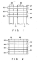
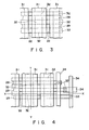
- Figs. 1 to 6 collectively show a semiconductor device in which the technical idea of the present invention is applied to the EPROM cell structure.
- a floating gate electrode pattern 201 is formed in a memory cell-forming region on the surface of, for example, a p-type silicon substrate 21 with a gate insulation film 23 interposed therebetween.
- the pattern 201 is positioned on an element isolating region 22. Then, one of the element isolating regions 22 is removed in self-alignment with the floating gate electrode pattern 201, followed by forming a diffusion layer region in which a silicide layer 29, including diffusion layers 27 and 207, is to be formed by self-aligned manner.
- a first diffusion layer 27 and a second diffusion layer 207 are formed, followed by a silicide layer 29, formed on layers 27 and 207 in self-aligned manner, as shown in Fig. 2.
- an insulating layer 30 is selectively formed to cover only the silicide layer 29, followed by forming a control gate electrode 31 and a floating gate electrode 32.
- insulating films 25 and 26 are interposed between the control gate electrode 31 and the floating gate electrode 32, and the control gate electrode 31 extends parallel with the shorter side of the floating gate electrode 32.
- the width of the floating gate electrode in the direction of the longer side is approximately equal to the width of the control gate electrode.
- desired contact holes 33 and the metal wiring layers 34 are formed as shown in Fig. 4 so as to obtain the final structure.
- reference numeral 35 in Figs. 5 and 6 denotes an insulating cover layer.
- the element isolation region 22 is formed in self-alignment with the floating gate electrode pattern 201.
- the silicide layer 29 having a low electrical resistance is formed in a self-aligned fashion in parallel with the longer side of the floating gate electrode 32.
- the control gate electrode 31 is formed in parallel with the shorter side of the floating gate electrode 32.
- the use of the silicide layer 29, having a low resistance permits elimination of the contact hole, though a single contact hole is required for every two cells in the conventional cell structure, making it possible to further miniaturize the unit cell area.
- a contact hole is not present substantially within the memory cell, with the result that a defect relating to the formation of the contact hole is not generated and, thus, a marked improvement in the yield of the semiconductor memory can be achieved.
- decoding is performed with the first diffusion layer 27 adjacent to the floating gate to be written on the side of a higher impurity concentration used as the drain and the second diffusion layer 207 adjacent to the said floating gate on a lower impurity concentration side used as the source.
- the floating gate electrode 32 is located between the first diffusion layer 27 and the second diffusion layer 207 in the present invention. It is possible to form the first diffusion layer 27 and the second diffusion layer 207 such that the impurity concentration in that part of the second diffusion layer 207 which is positioned adjacent to the floating gate electrode 32 is many of times lower than the impurity concentration in that part of the first diffusion layer 27 which is positioned adjacent to the floating gate electrode 32. In this case, the region of low impurity concentration, which is positioned adjacent to the floating gate electrode 32 in the second diffusion layer 207, can be formed 0.7 microns or less apart from the floating gate electrode 32 horizontally.
- control gate electrode 31 connected to a single word line, at 2 to 2.5 times as much as the total length of the shorter sides of the floating gate electrodes 32 belonging to said single word line.
- first diffusion layer 27 and the second diffusion layer 207 are formed in a self-aligned fashion along the longer side of the floating gate electrode.
- portion of the first diffusion layer 27 which is positioned adjacent to the floating gate electrode 32 to contain arsenic.
- portion of the second diffusion layer 207 which is positioned adjacent to the floating gate electrode 32 to contain phosphorus.
- the insulating layer 30, interposed between the wiring layer for the first and second diffusion layers and the wiring layer for the control gate electrode to include a film prepared by thermal oxidation of the wiring layer for the first diffusion layer 27 and the second diffusion layer 207.
- the insulating film 30 formed on the silicide film 29, covering the first diffusion layer 27 and the second diffusion layer 207 to consist of an oxide film having a thickness of 1,500 ⁇ or more.
- the floating gate electrode 32 may consist of a polysilicon layer.
- the wiring layer for the control gate electrode 31 may consist of a polysilicon layer, a silicide layer or a combination of a polysilicon layer and a silicide layer.
- the insulating films 25 and 26 formed on the floating gate electrode 32 to consist of an oxide film prepared by oxidizing a polysilicon layer.
- the insulating films 25 and 26 formed on the floating gate electrode 32 may be of a laminate structure consisting of a silicon oxide film and a silicon nitride film.
- insulating films 251, 26 and 252 are formed between the floating gate electrode 32 and the control gate electrode 31, as shown in Fig. 7.
- these insulating films 251, 26 and 252 are formed of an oxide film prepared by oxidizing a polysilicon film, a silicon nitride film and a silicon oxide film, respectively.
- the technical idea of the present invention is applied to an EPROM.
- the source diffusion layer and the drain diffusion layer of a nonvolatile memory cell are formed in parallel with each other along the longer side of the floating gate electrode.
- the control gate electrode is formed in parallel with the shorter side of the floating gate electrode.
- the source diffusion layer and the drain diffusion layer extend across the wiring layer for the control gate electrode at right angles.
- the length in the longer side of the floating gate electrode is set equal to the width of the control gate electrode.
- a silicide layer having a low electrical resistance is used for forming the wiring layers for the source and drain such that it is possible to omit a contact hole.
- the unit cell size can occupy the smallest area determinable by the element separating capability and the distance between adjacent gates.
- This particular construction permits marked miniaturization of the unit cell size, making it possible to provide a semiconductor memory having a large capacity.
- diffusion layers having the floating gate electrode sandwiched therebetween are formed with different impurity concentrations, i.e., a so-called "assymetrical drain structure", making it possible to sufficiently prevent erroneous information writing in the adjacent cell.
Landscapes
- Semiconductor Memories (AREA)
- Non-Volatile Memory (AREA)
Applications Claiming Priority (2)
| Application Number | Priority Date | Filing Date | Title |
|---|---|---|---|
| JP63240002A JP2755613B2 (ja) | 1988-09-26 | 1988-09-26 | 半導体装置 |
| JP240002/88 | 1988-09-26 |
Publications (3)
| Publication Number | Publication Date |
|---|---|
| EP0364769A2 true EP0364769A2 (de) | 1990-04-25 |
| EP0364769A3 EP0364769A3 (en) | 1990-05-02 |
| EP0364769B1 EP0364769B1 (de) | 1993-03-17 |
Family
ID=17053003
Family Applications (1)
| Application Number | Title | Priority Date | Filing Date |
|---|---|---|---|
| EP89117743A Expired - Lifetime EP0364769B1 (de) | 1988-09-26 | 1989-09-26 | Halbleiteranordnung mit einer Steuerelektrode, bestehend aus einer Mehrzahl von Schichten |
Country Status (5)
| Country | Link |
|---|---|
| US (1) | US5053840A (de) |
| EP (1) | EP0364769B1 (de) |
| JP (1) | JP2755613B2 (de) |
| KR (1) | KR930003560B1 (de) |
| DE (1) | DE68905425T2 (de) |
Cited By (14)
| Publication number | Priority date | Publication date | Assignee | Title |
|---|---|---|---|---|
| EP0468938A3 (en) * | 1990-07-24 | 1993-02-03 | Sgs-Thomson Microelectronics S.R.L. | Memory cell matrix and fabrication process |
| EP0471381A3 (en) * | 1990-08-15 | 1993-02-24 | Nec Corporation | Non-volatile memory and method for fabricating the same |
| EP0752721A3 (de) * | 1995-06-29 | 1997-06-11 | Sharp Kk | Nichtflüchtiger Halbleiterspeicher und Verfahren zur Steuerung und Verfahren zu seiner Herstellung |
| US5877054A (en) * | 1995-06-29 | 1999-03-02 | Sharp Kabushiki Kaisha | Method of making nonvolatile semiconductor memory |
| US5962889A (en) * | 1995-07-31 | 1999-10-05 | Sharp Kabushiki Kaisha | Nonvolatile semiconductor memory with a floating gate that has a bottom surface that is smaller than the upper surface |
| WO2000065654A1 (en) | 1999-04-23 | 2000-11-02 | Hrl Laboratories, Llc | Method and apparatus using silicide layer for protecting integrated circuits from reverse engineering |
| DE4113325C2 (de) * | 1990-04-30 | 2001-10-18 | Intel Corp | Verfahren zum Herstellen einer Speichermatrix aus Zellen mit schwimmenden Gates |
| WO2002045169A1 (de) * | 2000-11-28 | 2002-06-06 | Infineon Technologies Ag | Nichtflüchtige nor-eintransistor-halbleiterspeicherzelle |
| WO2002080275A3 (de) * | 2001-03-02 | 2003-01-30 | Infineon Technologies Ag | Speicherzellenarrays und deren herstellungssverfahren |
| US6667245B2 (en) | 1999-11-10 | 2003-12-23 | Hrl Laboratories, Llc | CMOS-compatible MEM switches and method of making |
| US6740942B2 (en) | 2001-06-15 | 2004-05-25 | Hrl Laboratories, Llc. | Permanently on transistor implemented using a double polysilicon layer CMOS process with buried contact |
| US6791191B2 (en) | 2001-01-24 | 2004-09-14 | Hrl Laboratories, Llc | Integrated circuits protected against reverse engineering and method for fabricating the same using vias without metal terminations |
| US6897535B2 (en) | 2002-05-14 | 2005-05-24 | Hrl Laboratories, Llc | Integrated circuit with reverse engineering protection |
| DE112012002648B4 (de) | 2011-06-27 | 2021-09-30 | International Business Machines Corporation | Lokale Zwischenverbindung mit einem niedrigen Profil und Verfahren zum Herstellen derselben |
Families Citing this family (24)
| Publication number | Priority date | Publication date | Assignee | Title |
|---|---|---|---|---|
| US5304829A (en) * | 1989-01-17 | 1994-04-19 | Kabushiki Kaisha Toshiba | Nonvolatile semiconductor device |
| JP2793722B2 (ja) * | 1991-01-29 | 1998-09-03 | 富士通株式会社 | 不揮発性半導体記憶装置およびその製造方法 |
| US5789298A (en) * | 1996-11-04 | 1998-08-04 | Advanced Micro Devices, Inc. | High performance mosfet structure having asymmetrical spacer formation and method of making the same |
| US6091100A (en) * | 1998-02-06 | 2000-07-18 | Texas Instruments - Acer Incorporated | High density NAND structure nonvolatile memories |
| JP3264241B2 (ja) | 1998-02-10 | 2002-03-11 | 日本電気株式会社 | 半導体装置の製造方法 |
| DE19808182C1 (de) * | 1998-02-26 | 1999-08-12 | Siemens Ag | Elektrisch programmierbare Speicherzellenanordnung und ein Verfahren zu deren Herstellung |
| US6020606A (en) * | 1998-03-20 | 2000-02-01 | United Silicon Incorporated | Structure of a memory cell |
| KR100295136B1 (ko) * | 1998-04-13 | 2001-09-17 | 윤종용 | 불휘발성메모리장치및그제조방법 |
| JP3097657B2 (ja) * | 1998-05-13 | 2000-10-10 | 日本電気株式会社 | 半導体記憶装置とその製造方法 |
| US7217977B2 (en) | 2004-04-19 | 2007-05-15 | Hrl Laboratories, Llc | Covert transformation of transistor properties as a circuit protection method |
| US6815816B1 (en) | 2000-10-25 | 2004-11-09 | Hrl Laboratories, Llc | Implanted hidden interconnections in a semiconductor device for preventing reverse engineering |
| DE10062245A1 (de) * | 2000-12-14 | 2002-07-04 | Infineon Technologies Ag | Nichtflüchtige Halbleiterspeicherzelle sowie dazugehörige Halbleiterschaltungsanordnung und Verfahren zu deren Herstellung |
| US7294935B2 (en) | 2001-01-24 | 2007-11-13 | Hrl Laboratories, Llc | Integrated circuits protected against reverse engineering and method for fabricating the same using an apparent metal contact line terminating on field oxide |
| US6774413B2 (en) | 2001-06-15 | 2004-08-10 | Hrl Laboratories, Llc | Integrated circuit structure with programmable connector/isolator |
| KR100485486B1 (ko) * | 2002-09-19 | 2005-04-27 | 동부아남반도체 주식회사 | 플래시 메모리 셀의 구조 및 그 제조 방법 |
| US7049667B2 (en) | 2002-09-27 | 2006-05-23 | Hrl Laboratories, Llc | Conductive channel pseudo block process and circuit to inhibit reverse engineering |
| US6979606B2 (en) | 2002-11-22 | 2005-12-27 | Hrl Laboratories, Llc | Use of silicon block process step to camouflage a false transistor |
| WO2004055868A2 (en) | 2002-12-13 | 2004-07-01 | Hrl Laboratories, Llc | Integrated circuit modification using well implants |
| US7242063B1 (en) | 2004-06-29 | 2007-07-10 | Hrl Laboratories, Llc | Symmetric non-intrusive and covert technique to render a transistor permanently non-operable |
| US8168487B2 (en) | 2006-09-28 | 2012-05-01 | Hrl Laboratories, Llc | Programmable connection and isolation of active regions in an integrated circuit using ambiguous features to confuse a reverse engineer |
| US9276011B2 (en) | 2013-03-15 | 2016-03-01 | Micron Technology, Inc. | Cell pillar structures and integrated flows |
| US9064970B2 (en) | 2013-03-15 | 2015-06-23 | Micron Technology, Inc. | Memory including blocking dielectric in etch stop tier |
| US9437604B2 (en) | 2013-11-01 | 2016-09-06 | Micron Technology, Inc. | Methods and apparatuses having strings of memory cells including a metal source |
| US9608000B2 (en) * | 2015-05-27 | 2017-03-28 | Micron Technology, Inc. | Devices and methods including an etch stop protection material |
Family Cites Families (8)
| Publication number | Priority date | Publication date | Assignee | Title |
|---|---|---|---|---|
| US4151021A (en) * | 1977-01-26 | 1979-04-24 | Texas Instruments Incorporated | Method of making a high density floating gate electrically programmable ROM |
| US4377818A (en) * | 1978-11-02 | 1983-03-22 | Texas Instruments Incorporated | High density electrically programmable ROM |
| US4267632A (en) * | 1979-10-19 | 1981-05-19 | Intel Corporation | Process for fabricating a high density electrically programmable memory array |
| JPS59126674A (ja) * | 1983-01-10 | 1984-07-21 | Toshiba Corp | 情報記憶用半導体装置 |
| JPS60147165A (ja) * | 1984-01-12 | 1985-08-03 | Nec Corp | 不揮発性半導体メモリセル及びその使用方法 |
| JPS60182174A (ja) * | 1984-02-28 | 1985-09-17 | Nec Corp | 不揮発性半導体メモリ |
| US4763177A (en) * | 1985-02-19 | 1988-08-09 | Texas Instruments Incorporated | Read only memory with improved channel length isolation and method of forming |
| US4597060A (en) * | 1985-05-01 | 1986-06-24 | Texas Instruments Incorporated | EPROM array and method for fabricating |
-
1988
- 1988-09-26 JP JP63240002A patent/JP2755613B2/ja not_active Expired - Fee Related
-
1989
- 1989-09-20 US US07/409,687 patent/US5053840A/en not_active Expired - Lifetime
- 1989-09-26 EP EP89117743A patent/EP0364769B1/de not_active Expired - Lifetime
- 1989-09-26 DE DE8989117743T patent/DE68905425T2/de not_active Expired - Fee Related
- 1989-09-26 KR KR1019890013817A patent/KR930003560B1/ko not_active Expired - Fee Related
Cited By (19)
| Publication number | Priority date | Publication date | Assignee | Title |
|---|---|---|---|---|
| DE4113325C2 (de) * | 1990-04-30 | 2001-10-18 | Intel Corp | Verfahren zum Herstellen einer Speichermatrix aus Zellen mit schwimmenden Gates |
| EP0468938A3 (en) * | 1990-07-24 | 1993-02-03 | Sgs-Thomson Microelectronics S.R.L. | Memory cell matrix and fabrication process |
| US5279982A (en) * | 1990-07-24 | 1994-01-18 | Sgs-Thomson Microelectronics S.R.L. | Method for fabricating memory cell matrix having parallel source and drain interconnection metal lines formed on the substrate and topped by orthogonally oriented gate interconnection parallel metal lines |
| EP0471381A3 (en) * | 1990-08-15 | 1993-02-24 | Nec Corporation | Non-volatile memory and method for fabricating the same |
| USRE37199E1 (en) * | 1995-06-29 | 2001-05-29 | Sharp Kabushiki Kaisha | Method of making nonvolatile semiconductor memory |
| US6101128A (en) * | 1995-06-29 | 2000-08-08 | Sharp Kabushiki Kaisha | Nonvolatile semiconductor memory and driving method and fabrication method of the same |
| US5877054A (en) * | 1995-06-29 | 1999-03-02 | Sharp Kabushiki Kaisha | Method of making nonvolatile semiconductor memory |
| EP0752721A3 (de) * | 1995-06-29 | 1997-06-11 | Sharp Kk | Nichtflüchtiger Halbleiterspeicher und Verfahren zur Steuerung und Verfahren zu seiner Herstellung |
| US5962889A (en) * | 1995-07-31 | 1999-10-05 | Sharp Kabushiki Kaisha | Nonvolatile semiconductor memory with a floating gate that has a bottom surface that is smaller than the upper surface |
| WO2000065654A1 (en) | 1999-04-23 | 2000-11-02 | Hrl Laboratories, Llc | Method and apparatus using silicide layer for protecting integrated circuits from reverse engineering |
| US6667245B2 (en) | 1999-11-10 | 2003-12-23 | Hrl Laboratories, Llc | CMOS-compatible MEM switches and method of making |
| WO2002045169A1 (de) * | 2000-11-28 | 2002-06-06 | Infineon Technologies Ag | Nichtflüchtige nor-eintransistor-halbleiterspeicherzelle |
| US6791191B2 (en) | 2001-01-24 | 2004-09-14 | Hrl Laboratories, Llc | Integrated circuits protected against reverse engineering and method for fabricating the same using vias without metal terminations |
| WO2002080275A3 (de) * | 2001-03-02 | 2003-01-30 | Infineon Technologies Ag | Speicherzellenarrays und deren herstellungssverfahren |
| US6686242B2 (en) | 2001-03-02 | 2004-02-03 | Infineon Technologies Ag | Method for producing metallic bit lines for memory cell arrays, method for producing memory cell arrays and memory cell array |
| US6740942B2 (en) | 2001-06-15 | 2004-05-25 | Hrl Laboratories, Llc. | Permanently on transistor implemented using a double polysilicon layer CMOS process with buried contact |
| US6897535B2 (en) | 2002-05-14 | 2005-05-24 | Hrl Laboratories, Llc | Integrated circuit with reverse engineering protection |
| US7008873B2 (en) | 2002-05-14 | 2006-03-07 | Hrl Laboratories, Llc | Integrated circuit with reverse engineering protection |
| DE112012002648B4 (de) | 2011-06-27 | 2021-09-30 | International Business Machines Corporation | Lokale Zwischenverbindung mit einem niedrigen Profil und Verfahren zum Herstellen derselben |
Also Published As
| Publication number | Publication date |
|---|---|
| JP2755613B2 (ja) | 1998-05-20 |
| EP0364769A3 (en) | 1990-05-02 |
| KR930003560B1 (ko) | 1993-05-06 |
| EP0364769B1 (de) | 1993-03-17 |
| US5053840A (en) | 1991-10-01 |
| JPH0287578A (ja) | 1990-03-28 |
| KR900005470A (ko) | 1990-04-14 |
| DE68905425D1 (de) | 1993-04-22 |
| DE68905425T2 (de) | 1993-09-09 |
Similar Documents
| Publication | Publication Date | Title |
|---|---|---|
| EP0364769A2 (de) | Halbleiteranordnung mit einer Steuerelektrode, bestehend aus einer Mehrzahl von Schichten | |
| US5629541A (en) | Semiconductor memory device constituted by single transistor type non-volatile cells and facilitated for both electrical erasing and writing of data | |
| US4451904A (en) | Semiconductor memory device | |
| KR930009139B1 (ko) | 불휘발성 반도체장치 | |
| US4737835A (en) | Read only memory semiconductor device | |
| US5851880A (en) | Method of making nonvolatile memory elements with selector transistors | |
| US5200636A (en) | Semiconductor device having E2 PROM and EPROM in one chip | |
| US6291855B1 (en) | Cell of flash memory device | |
| KR100406091B1 (ko) | 반도체 장치 | |
| US5436480A (en) | Integrated circuit interconnection programmable and erasable by a plurality of intersecting control traces | |
| US6952031B2 (en) | Nonvolatile semiconductor memory and method of operating the same | |
| EP0432792B1 (de) | Nichtflüchtige Halbleiterspeicheranordnung und Verfahren zu ihrer Herstellung | |
| US6573557B1 (en) | EEPROM cell having reduced cell area | |
| EP0302659B1 (de) | Halbleiterspeichervorrichtung und Herstellungsverfahren | |
| JP4031178B2 (ja) | 半導体高抵抗素子の製造方法 | |
| JPS6325978A (ja) | 半導体集積回路装置 | |
| JP3002009B2 (ja) | 半導体装置 | |
| JPS6352478A (ja) | 半導体集積回路装置 | |
| JPS63166A (ja) | 不揮発性半導体記憶装置 | |
| JPH02180079A (ja) | 半導体不揮発性記憶装置とその製造方法 | |
| KR900001764B1 (ko) | 반도체 기억장치 | |
| JP2797466B2 (ja) | 不揮発性半導体記憶装置 | |
| JPS59132160A (ja) | 半導体装置 | |
| JPS6214473A (ja) | 半導体不揮発性記憶装置およびその書込み方法 | |
| JPS6246576A (ja) | 半導体集積回路装置 |
Legal Events
| Date | Code | Title | Description |
|---|---|---|---|
| PUAI | Public reference made under article 153(3) epc to a published international application that has entered the european phase |
Free format text: ORIGINAL CODE: 0009012 |
|
| PUAL | Search report despatched |
Free format text: ORIGINAL CODE: 0009013 |
|
| 17P | Request for examination filed |
Effective date: 19890926 |
|
| AK | Designated contracting states |
Kind code of ref document: A2 Designated state(s): DE FR GB |
|
| AK | Designated contracting states |
Kind code of ref document: A3 Designated state(s): DE FR GB |
|
| 17Q | First examination report despatched |
Effective date: 19920508 |
|
| GRAA | (expected) grant |
Free format text: ORIGINAL CODE: 0009210 |
|
| AK | Designated contracting states |
Kind code of ref document: B1 Designated state(s): DE FR GB |
|
| REF | Corresponds to: |
Ref document number: 68905425 Country of ref document: DE Date of ref document: 19930422 |
|
| ET | Fr: translation filed | ||
| PLBE | No opposition filed within time limit |
Free format text: ORIGINAL CODE: 0009261 |
|
| STAA | Information on the status of an ep patent application or granted ep patent |
Free format text: STATUS: NO OPPOSITION FILED WITHIN TIME LIMIT |
|
| 26N | No opposition filed | ||
| PGFP | Annual fee paid to national office [announced via postgrant information from national office to epo] |
Ref country code: FR Payment date: 19970909 Year of fee payment: 9 |
|
| PGFP | Annual fee paid to national office [announced via postgrant information from national office to epo] |
Ref country code: DE Payment date: 19971010 Year of fee payment: 9 |
|
| REG | Reference to a national code |
Ref country code: GB Ref legal event code: 746 Effective date: 19980915 |
|
| PG25 | Lapsed in a contracting state [announced via postgrant information from national office to epo] |
Ref country code: FR Free format text: LAPSE BECAUSE OF NON-PAYMENT OF DUE FEES Effective date: 19990531 |
|
| PG25 | Lapsed in a contracting state [announced via postgrant information from national office to epo] |
Ref country code: DE Free format text: LAPSE BECAUSE OF NON-PAYMENT OF DUE FEES Effective date: 19990701 |
|
| REG | Reference to a national code |
Ref country code: FR Ref legal event code: ST |
|
| REG | Reference to a national code |
Ref country code: GB Ref legal event code: IF02 |
|
| PGFP | Annual fee paid to national office [announced via postgrant information from national office to epo] |
Ref country code: GB Payment date: 20050921 Year of fee payment: 17 |
|
| GBPC | Gb: european patent ceased through non-payment of renewal fee |
Effective date: 20060926 |
|
| PG25 | Lapsed in a contracting state [announced via postgrant information from national office to epo] |
Ref country code: GB Free format text: LAPSE BECAUSE OF NON-PAYMENT OF DUE FEES Effective date: 20060926 |