EP0364962A1 - Dispositif pour surveiller la température lors du brasage tendre à la vague de groupes de construction plans - Google Patents
Dispositif pour surveiller la température lors du brasage tendre à la vague de groupes de construction plans Download PDFInfo
- Publication number
- EP0364962A1 EP0364962A1 EP89119272A EP89119272A EP0364962A1 EP 0364962 A1 EP0364962 A1 EP 0364962A1 EP 89119272 A EP89119272 A EP 89119272A EP 89119272 A EP89119272 A EP 89119272A EP 0364962 A1 EP0364962 A1 EP 0364962A1
- Authority
- EP
- European Patent Office
- Prior art keywords
- soldering
- temperature
- monitoring
- wave
- pyrometer
- Prior art date
- Legal status (The legal status is an assumption and is not a legal conclusion. Google has not performed a legal analysis and makes no representation as to the accuracy of the status listed.)
- Withdrawn
Links
Images
Classifications
-
- H—ELECTRICITY
- H05—ELECTRIC TECHNIQUES NOT OTHERWISE PROVIDED FOR
- H05K—PRINTED CIRCUITS; CASINGS OR CONSTRUCTIONAL DETAILS OF ELECTRIC APPARATUS; MANUFACTURE OF ASSEMBLAGES OF ELECTRICAL COMPONENTS
- H05K3/00—Apparatus or processes for manufacturing printed circuits
- H05K3/30—Assembling printed circuits with electric components, e.g. with resistors
- H05K3/32—Assembling printed circuits with electric components, e.g. with resistors electrically connecting electric components or wires to printed circuits
- H05K3/34—Assembling printed circuits with electric components, e.g. with resistors electrically connecting electric components or wires to printed circuits by soldering
- H05K3/3465—Application of solder
- H05K3/3468—Application of molten solder, e.g. dip soldering
-
- B—PERFORMING OPERATIONS; TRANSPORTING
- B23—MACHINE TOOLS; METAL-WORKING NOT OTHERWISE PROVIDED FOR
- B23K—SOLDERING OR UNSOLDERING; WELDING; CLADDING OR PLATING BY SOLDERING OR WELDING; CUTTING BY APPLYING HEAT LOCALLY, e.g. FLAME CUTTING; WORKING BY LASER BEAM
- B23K1/00—Soldering, e.g. brazing, or unsoldering
- B23K1/08—Soldering by means of dipping in molten solder
- B23K1/085—Wave soldering
-
- B—PERFORMING OPERATIONS; TRANSPORTING
- B23—MACHINE TOOLS; METAL-WORKING NOT OTHERWISE PROVIDED FOR
- B23K—SOLDERING OR UNSOLDERING; WELDING; CLADDING OR PLATING BY SOLDERING OR WELDING; CUTTING BY APPLYING HEAT LOCALLY, e.g. FLAME CUTTING; WORKING BY LASER BEAM
- B23K2101/00—Articles made by soldering, welding or cutting
- B23K2101/36—Electric or electronic devices
- B23K2101/40—Semiconductor devices
-
- H—ELECTRICITY
- H05—ELECTRIC TECHNIQUES NOT OTHERWISE PROVIDED FOR
- H05K—PRINTED CIRCUITS; CASINGS OR CONSTRUCTIONAL DETAILS OF ELECTRIC APPARATUS; MANUFACTURE OF ASSEMBLAGES OF ELECTRICAL COMPONENTS
- H05K1/00—Printed circuits
- H05K1/02—Details
- H05K1/0201—Thermal arrangements, e.g. for cooling, heating or preventing overheating
-
- H—ELECTRICITY
- H05—ELECTRIC TECHNIQUES NOT OTHERWISE PROVIDED FOR
- H05K—PRINTED CIRCUITS; CASINGS OR CONSTRUCTIONAL DETAILS OF ELECTRIC APPARATUS; MANUFACTURE OF ASSEMBLAGES OF ELECTRICAL COMPONENTS
- H05K2203/00—Indexing scheme relating to apparatus or processes for manufacturing printed circuits covered by H05K3/00
- H05K2203/16—Inspection; Monitoring; Aligning
- H05K2203/163—Monitoring a manufacturing process
-
- H—ELECTRICITY
- H05—ELECTRIC TECHNIQUES NOT OTHERWISE PROVIDED FOR
- H05K—PRINTED CIRCUITS; CASINGS OR CONSTRUCTIONAL DETAILS OF ELECTRIC APPARATUS; MANUFACTURE OF ASSEMBLAGES OF ELECTRICAL COMPONENTS
- H05K2203/00—Indexing scheme relating to apparatus or processes for manufacturing printed circuits covered by H05K3/00
- H05K2203/30—Details of processes not otherwise provided for in H05K2203/01 - H05K2203/17
- H05K2203/304—Protecting a component during manufacturing
Definitions
- the invention relates to an arrangement for monitoring the temperature when wave soldering flat assemblies.
- the object of the present invention is to create an arrangement by which the overheating of printed circuit boards during soldering is avoided.
- the arrangement according to the invention is designed in such a way that a pyrometer with a sheet of metal shielded from the surge of solder upwards is arranged transversely to the soldering direction and diagonally upwards against the flat module to be soldered, immediately after the surge nozzle, that the pyrometer has a limit indicator connected, which responds when a permissible limit temperature of the printed circuit board is exceeded.
- an alarm device e.g. in the form of a signal lamp or a safety device, e.g. to stop the system. It is also possible for the parameters, e.g. to influence the soldering speed.
- the invention is explained in more detail using the exemplary embodiment.
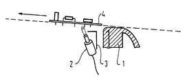
- the printed circuit board 4 equipped with electronic components is guided over a surge nozzle 1 for the purpose of soldering the components.
- a pyrometer 2 is arranged below the printed circuit board and is oriented transversely to the direction of movement and obliquely upwards towards the printed circuit board.
- the shielding plate 3 is provided, which covers the pyrometer above and to the side of the solder Walls out. In order to avoid contamination of the pyrometer's radiation receiver, an air purge can be provided around the pyrometer.
Landscapes
- Engineering & Computer Science (AREA)
- Mechanical Engineering (AREA)
- Manufacturing & Machinery (AREA)
- Microelectronics & Electronic Packaging (AREA)
- Electric Connection Of Electric Components To Printed Circuits (AREA)
Applications Claiming Priority (2)
| Application Number | Priority Date | Filing Date | Title |
|---|---|---|---|
| DE3835650 | 1988-10-19 | ||
| DE3835650 | 1988-10-19 |
Publications (1)
| Publication Number | Publication Date |
|---|---|
| EP0364962A1 true EP0364962A1 (fr) | 1990-04-25 |
Family
ID=6365481
Family Applications (1)
| Application Number | Title | Priority Date | Filing Date |
|---|---|---|---|
| EP89119272A Withdrawn EP0364962A1 (fr) | 1988-10-19 | 1989-10-17 | Dispositif pour surveiller la température lors du brasage tendre à la vague de groupes de construction plans |
Country Status (3)
| Country | Link |
|---|---|
| US (1) | US4982177A (fr) |
| EP (1) | EP0364962A1 (fr) |
| CA (1) | CA2000895A1 (fr) |
Cited By (1)
| Publication number | Priority date | Publication date | Assignee | Title |
|---|---|---|---|---|
| EP0405408A3 (en) * | 1989-06-29 | 1992-07-22 | Siemens Aktiengesellschaft | Method and apparatus of making contact to a semiconductor component by use as a laser beam, and resulting device |
Citations (2)
| Publication number | Priority date | Publication date | Assignee | Title |
|---|---|---|---|---|
| EP0118091A1 (fr) * | 1983-02-28 | 1984-09-12 | Electrovert Ltd. | Machine automatique pour souder par ondes |
| EP0279011A1 (fr) * | 1986-07-01 | 1988-08-24 | Electrovert Ltd. | Appareil de chauffage en plusieurs phases, en particulier pour le soudage des circuits imprimés |
Family Cites Families (5)
| Publication number | Priority date | Publication date | Assignee | Title |
|---|---|---|---|---|
| US3750134A (en) * | 1971-02-11 | 1973-07-31 | Package Machinery Co | Plastic injection molding machine monitor |
| US4447805A (en) * | 1981-02-23 | 1984-05-08 | Mitsubishi Kasei Kogyo Kabushiki Kaisha | Apparatus for measuring temperature of coke ovens |
| JPS60174833A (ja) * | 1984-02-20 | 1985-09-09 | Nippon Steel Corp | 熱鋼板の冷却方法 |
| FR2572970B1 (fr) * | 1984-11-15 | 1987-02-13 | Outillages Scient Lab | Dispositif chauffant de generation d'une vague de soudure pour machine de soudage a la vague |
| US4890781A (en) * | 1988-08-04 | 1990-01-02 | Texas Instruments Incorporated | Automated flow solder machine |
-
1989
- 1989-10-17 EP EP89119272A patent/EP0364962A1/fr not_active Withdrawn
- 1989-10-17 CA CA002000895A patent/CA2000895A1/fr not_active Abandoned
- 1989-10-19 US US07/424,072 patent/US4982177A/en not_active Expired - Fee Related
Patent Citations (3)
| Publication number | Priority date | Publication date | Assignee | Title |
|---|---|---|---|---|
| EP0118091A1 (fr) * | 1983-02-28 | 1984-09-12 | Electrovert Ltd. | Machine automatique pour souder par ondes |
| EP0269822A1 (fr) * | 1983-02-28 | 1988-06-08 | Electrovert Ltd. | Machine automatique pour souder par ondes |
| EP0279011A1 (fr) * | 1986-07-01 | 1988-08-24 | Electrovert Ltd. | Appareil de chauffage en plusieurs phases, en particulier pour le soudage des circuits imprimés |
Cited By (1)
| Publication number | Priority date | Publication date | Assignee | Title |
|---|---|---|---|---|
| EP0405408A3 (en) * | 1989-06-29 | 1992-07-22 | Siemens Aktiengesellschaft | Method and apparatus of making contact to a semiconductor component by use as a laser beam, and resulting device |
Also Published As
| Publication number | Publication date |
|---|---|
| US4982177A (en) | 1991-01-01 |
| CA2000895A1 (fr) | 1990-04-19 |
Similar Documents
| Publication | Publication Date | Title |
|---|---|---|
| EP0012319B1 (fr) | Procédé et gabarit pour la fixation de composants ayant des pattes de connexion plates sur des substrats conducteurs | |
| DE112019008023B4 (de) | Verfahren zum Installieren eines Bildsensors einer Kamera | |
| EP1486104A2 (fr) | Procede pour equiper et braser une carte de circuits imprimes, four de refusion et carte de circuits imprimes adaptee a un tel procede | |
| DE68905001T2 (de) | Verfahren zum flussmittelfreien loeten. | |
| Mearig et al. | An overview of manufacturing BGA technology | |
| DE3022310A1 (de) | Vorrichtung und verfahren zum ausbauen eines elektronischen modulbausteins | |
| DE102008053182A1 (de) | Elektronische Baugruppe mit Thermosicherung | |
| DE3209914A1 (de) | Hoergeraet mit einer verstaerkerschaltung | |
| EP2647270A1 (fr) | Procédé de brasage et dispositif de brasage associé | |
| DE69803216T2 (de) | Gedruckte leiterplatten | |
| WO2009103515A2 (fr) | Agencement de cartes de circuits imprimés et module de connexion électrique | |
| EP4271146A1 (fr) | Procédé d'impression de masque ayant des paramètres optimisés et dispositif | |
| DE2622324B2 (de) | Verfahren zur Herstellung eines genau abgeglichenen elektrischen Netzwerkes | |
| EP0364962A1 (fr) | Dispositif pour surveiller la température lors du brasage tendre à la vague de groupes de construction plans | |
| DE2343235B2 (de) | Verfahren zur Befestigung und Kontaktierung von elektrischen Subminiatur-Bauelementen auf gedruckten Schaltungen | |
| EP0307766A1 (fr) | Circuit imprimé permettant le montage de composants SMD | |
| EP0121910B1 (fr) | Pistolet à désouder | |
| EP2663070A1 (fr) | Composant de capteur d'images pour une caméra, ainsi que procédé et outil de pliage pour sa fabrication | |
| DE2017422C3 (de) | Selbsttätige Sicherheitsschaltung zur Überwachung des Leistungsschaltgliedes eines elektrischen Stromverbrauchers | |
| DE4212068C1 (fr) | ||
| DE69104580T2 (de) | Anordnung und Verfahren zur Anordnung für den Einbau von elektronischen Bauelementen auf flexiblen gedruckten Schaltungen. | |
| DE3510000A1 (de) | Thermoplastisches loetmittel und verfahren und vorrichtung zu dessen verwendung | |
| DE4205789A1 (de) | Lichtquelle mit mindestens einem lichtemittierenden bauelement und einer vorgeschalteten schutzeinrichtung | |
| EP3150033B1 (fr) | Méthode de mise en contact avec une carte de circuit imprimé souple | |
| DE19509786A1 (de) | Verfahren zum Verlöten von elektronischen Bauelementen auf einer Leiterplatte |
Legal Events
| Date | Code | Title | Description |
|---|---|---|---|
| PUAI | Public reference made under article 153(3) epc to a published international application that has entered the european phase |
Free format text: ORIGINAL CODE: 0009012 |
|
| AK | Designated contracting states |
Kind code of ref document: A1 Designated state(s): AT BE CH DE FR GB IT LI NL |
|
| 17P | Request for examination filed |
Effective date: 19900528 |
|
| RAP1 | Party data changed (applicant data changed or rights of an application transferred) |
Owner name: SIEMENS NIXDORF INFORMATIONSSYSTEME AG |
|
| STAA | Information on the status of an ep patent application or granted ep patent |
Free format text: STATUS: THE APPLICATION HAS BEEN WITHDRAWN |
|
| 18W | Application withdrawn |
Withdrawal date: 19911008 |
|
| EN | Fr: translation not filed |