EP0365039B1 - Guide d'onde optique et générateur d'harmonique du second ordre - Google Patents
Guide d'onde optique et générateur d'harmonique du second ordre Download PDFInfo
- Publication number
- EP0365039B1 EP0365039B1 EP89119535A EP89119535A EP0365039B1 EP 0365039 B1 EP0365039 B1 EP 0365039B1 EP 89119535 A EP89119535 A EP 89119535A EP 89119535 A EP89119535 A EP 89119535A EP 0365039 B1 EP0365039 B1 EP 0365039B1
- Authority
- EP
- European Patent Office
- Prior art keywords
- substrate
- optical waveguide
- harmonic generator
- waveguide
- periodically
- Prior art date
- Legal status (The legal status is an assumption and is not a legal conclusion. Google has not performed a legal analysis and makes no representation as to the accuracy of the status listed.)
- Expired - Lifetime
Links
Images






Classifications
-
- G—PHYSICS
- G02—OPTICS
- G02F—OPTICAL DEVICES OR ARRANGEMENTS FOR THE CONTROL OF LIGHT BY MODIFICATION OF THE OPTICAL PROPERTIES OF THE MEDIA OF THE ELEMENTS INVOLVED THEREIN; NON-LINEAR OPTICS; FREQUENCY-CHANGING OF LIGHT; OPTICAL LOGIC ELEMENTS; OPTICAL ANALOGUE/DIGITAL CONVERTERS
- G02F1/00—Devices or arrangements for the control of the intensity, colour, phase, polarisation or direction of light arriving from an independent light source, e.g. switching, gating or modulating; Non-linear optics
- G02F1/35—Non-linear optics
- G02F1/37—Non-linear optics for second-harmonic generation
- G02F1/377—Non-linear optics for second-harmonic generation in an optical waveguide structure
- G02F1/3775—Non-linear optics for second-harmonic generation in an optical waveguide structure with a periodic structure, e.g. domain inversion, for quasi-phase-matching [QPM]
-
- G—PHYSICS
- G02—OPTICS
- G02F—OPTICAL DEVICES OR ARRANGEMENTS FOR THE CONTROL OF LIGHT BY MODIFICATION OF THE OPTICAL PROPERTIES OF THE MEDIA OF THE ELEMENTS INVOLVED THEREIN; NON-LINEAR OPTICS; FREQUENCY-CHANGING OF LIGHT; OPTICAL LOGIC ELEMENTS; OPTICAL ANALOGUE/DIGITAL CONVERTERS
- G02F1/00—Devices or arrangements for the control of the intensity, colour, phase, polarisation or direction of light arriving from an independent light source, e.g. switching, gating or modulating; Non-linear optics
- G02F1/35—Non-linear optics
- G02F1/353—Frequency conversion, i.e. wherein a light beam is generated with frequency components different from those of the incident light beams
- G02F1/3544—Particular phase matching techniques
- G02F1/3548—Quasi phase matching [QPM], e.g. using a periodic domain inverted structure
-
- G—PHYSICS
- G02—OPTICS
- G02F—OPTICAL DEVICES OR ARRANGEMENTS FOR THE CONTROL OF LIGHT BY MODIFICATION OF THE OPTICAL PROPERTIES OF THE MEDIA OF THE ELEMENTS INVOLVED THEREIN; NON-LINEAR OPTICS; FREQUENCY-CHANGING OF LIGHT; OPTICAL LOGIC ELEMENTS; OPTICAL ANALOGUE/DIGITAL CONVERTERS
- G02F1/00—Devices or arrangements for the control of the intensity, colour, phase, polarisation or direction of light arriving from an independent light source, e.g. switching, gating or modulating; Non-linear optics
- G02F1/35—Non-linear optics
- G02F1/37—Non-linear optics for second-harmonic generation
- G02F1/374—Cherenkov radiation
-
- G—PHYSICS
- G02—OPTICS
- G02F—OPTICAL DEVICES OR ARRANGEMENTS FOR THE CONTROL OF LIGHT BY MODIFICATION OF THE OPTICAL PROPERTIES OF THE MEDIA OF THE ELEMENTS INVOLVED THEREIN; NON-LINEAR OPTICS; FREQUENCY-CHANGING OF LIGHT; OPTICAL LOGIC ELEMENTS; OPTICAL ANALOGUE/DIGITAL CONVERTERS
- G02F2202/00—Materials and properties
- G02F2202/20—LiNbO3, LiTaO3
Definitions
- the present invention relates generally to optical waveguide apparatus for use with an optical communication system, an optical integrated circuit and the like and, more particularly, is directed to a second harmonic generator of optical waveguide type based on Cerenkov radiation.
- An optical waveguide in an optical communication system, an optical integrated circuit and the like must be made of optical waveguide material having a refractive index as high as possible so that it can fully confine a waveguide light.
- an amorphous film such as Ta2O5 and Nb2O5
- a single crystal film of PLZT Pb-based Lanthanum-doped Zirconate Titanates
- chalcogenide such as As2S5
- Ta2O5 has a refractive index of 1.9 to 2.2; Nb2O5 has a refractive index of 2.1 to 2.3; PLZT has a refractive index of about 2.6; and chalcogenide has a refractive index higher than 2.3.
- the PLZT has to be grown as a single crystal film so that as a substrate for this film growing-process, there is used only a single crystal substrate such as sapphire and the like; chalcogenide-based material has high light absorption property in the area of visible light so that it can not make an optical waveguide which is used in the area of visible light; and Ta2O5 has a small refractive index compared with those of LiNbO3 substrate and LiTaO3 substrate which are frequently used in the optical IC so that it can not make an optical waveguide for such substrate.
- a thin film optical waveguide can not be formed on a substrate such as LiNbO3 and LiTaO3 so as to achieve low propagation loss ( ⁇ 1dB/cm) over a wide range from a near-infrared ray area to a visible light area.
- a second harmonic generator which generates, when supplied with a light having a frequency ⁇ , a second harmonic wave light of frequency 2 ⁇ .
- the wavelength region can be enlarged and, with the enlarged wavelength region, a laser apparatus is utilized in a wider variety of applications, and the use of laser light can be optimized in various technical fields. For example, in the optical recording and reproducing process and magneto-optical recording and reproducing process by use of laser light, it becomes possible to increase recording density by reducing the wavelength of laser beam.
- Applied Physics Letters 17 , 447 (1970) reported a second harmonic generator of Cerenkov radiation type in which a linear optical waveguide is formed on a non-linear single crystal substrate, and which is supplied with a fundamental wave to achieve a second harmonic wave radiation mode to generate a second harmonic wave from the substrate side.
- This type of second harmonic generator comprises a ZnO non-linear single crystal substrate and a ZnS polycrystal optical waveguide formed thereon and generates a second harmonic wave of 0.53 micrometer by use of a Nd:YAG laser having a wavelength of 1.06 micrometers.
- the waveguide thereof is made of polycrystalline material so that its propagation loss is large and a d constant of the ZnO substrate is small, which provides a considerably degenerated efficiency.
- Japanese Laid-Open Patent Gazette No. 61-189524 discloses a second harmonic generator.
- This previously-proposed second harmonic generator employs a LiNbO3 (hereinafter, simply referred to as LN) substrate which has an optical waveguide constitution by proton exchange.
- LN LiNbO3
- a semiconductor laser of 0.84 micrometer is utilized as a fundamental light source, and which is supplied with an input of about 100 mW for generating an SHG light of 1 to 2 mW.
- the most specific feature of the SHG element of this system lies in an automatic phase matching process.
- SHG efficiency is less than 1 to 2 % relative to the input of 100 mW, and it cannot achieve SHG efficiency of, for example, 10 % which is required in practice.
- the proton exchange-process is effective only for the LN substrate, and cannot be applied to other substrates such as LiTaO3 and KNbO3.
- the efficiency ⁇ has a relationship for a d constant of non-linear optical material, fundamental wave power density P ⁇ and mutual action length l ⁇ ⁇ d2 ⁇ P ⁇ ⁇ l Accordingly, in order to gain a high efficiency of second harmonic generator, a material having a large d constant must be used, the fundamental wave power density P ⁇ must be increased and the mutual action length l must be increased.
- the value of d constant is changed depending on the geometrical relation of its crystal azimuth and polarized wave direction of fundamental wave even in the same material.
- an X-cut crystal and a Y-cut crystal are etched during the proton exchange-process and the surfaces thereof are made coarse, whereby the LN as the non-linear single crystal substrate can utilize only the Z-cut crystal (substrate having a plane perpendicular to the z-axis extending along the c-axis) and utilize only the TM wave mode.
- the semiconductor laser is employed as the light source, a 1/2 wavelength plate must be provided between the semiconductor laser and the input end of the optical waveguide of the second harmonic generator so as to rotate the polarization direction of the laser light by 90 degrees.
- a refractive index difference ⁇ n between the waveguide and the substrate is about 0.14 at maximum. There is then a limit on the confinement of light, i.e. the maximum efficiency.
- the proton exchange-process is effective only for the LN and can not be applied to LiTaO3, KNbO3 or the like.
- the radiated SHG wave has a lateral spread angle of larger than 10 degrees and has a beam spot S of a crescent-shape. There is then presented a problem of a converging characteristic.
- An optical waveguide means comprising the features of the preamble of claim 1 is known from an article of D. H. Hensler et al., having the title "Optical Propagation in Sheet and Pattern Generated Films of Ta2O5", published in Applied Optics, Vol. 10, No. 5, May 1971, pp. 1037 - 1042.
- the optical waveguide means of this invention is defined by the features of claim 1. It differs from the just above mentioned waveguide means in that the amorphous thin film by which the optical waveguide is made, does not comprise Ta2O5 but also TiO2 in a range up to 60 atomic percent.
- the second harmonic generator of the present invention is characterized in that it uses an optical waveguide means according to claim 1, provided on a substrate which is a non-linear optical material.
- This second harmonic generator can be used to generate Cerenkov radiation when a fundamental wave of near-infrared rays is irradiated.
- this second harmonic generator comprises a substrate on the surface of which a periodically-poled region is formed, the overlap between the fundamental guidemode and the second harmonic radiation mode can be improved due to a special relationship between the thickness of the waveguide and the cycle of the periodically-poled region.
- the second harmonic generator of the present invention provides for an SHG light beam of excellent converging characteristics.
- an amorphous optical waveguide 2 was formed on a substrate 1.
- the amorphous optical waveguide 2 was formed such that TiO2 was doped to Ta2O5 by a doping amount in which Ti was in a range of from 0 to 60 atomic percents relative to the sum of Ti and Ta.
- the optical waveguide and second harmonic generator thus made present sufficient low propagation loss and large refractive index over a range from near-infrared rays to a visible light region.
- the refractive index n in the wavelength region of 0.6328 micrometer could be varied in a range of about 2.2 to 2.4 by selecting a doping amount of Ti.
- the optical waveguide 2 was formed of an optical waveguide in which TiO2 was doped to Ta2O5 so that, even when LN, for example, was utilized as the non-linear optical material substrate 1, a refractive index difference ⁇ n between the optical waveguide 2 and the substrate 1 could be increased sufficiently and that the maximum efficiency could be increased.
- the employment of d33 made the TM wave mode and the TE wave mode possible. Accordingly, if the TE wave mode was made and a semiconductor laser was used as a fundamental wave light source, a 1/2 wavelength plate, which was needed to couple the second harmonic generator in the TM wave mode could be removed.
- the substrate 1 is not limited to the LN substrate and might be made of a transparent substrate material having a heat-resisting property for a substrate temperature produced when the optical waveguide is deposited on the substrate by, for example, a chemical vapor deposition (CVD) process, freedom for selecting substrate material can be increased, and a material having a smaller refractive index can be used, which provides a more increased refractive index difference ⁇ n.
- CVD chemical vapor deposition
- the optical waveguide is an amorphous waveguide so that the propagation loss, increased by the existence of crystalline grain boundary, can be avoided.
- a second harmonic generator of high efficiency can be obtained and the optical waveguide can be easily formed as a ridge-type optical waveguide by a some suitable manufacturing-process.
- a fundamental waveguide 12 of TiO2-doped-Ta2O5 thin film is formed on an LiNbO3 non-linear optical crystal substrate 11 in which a periodically-poled region 10 is formed on the surface.
- an overlap between the fundamental guide mode and the second harmonic radiation mode is arranged to present features different from those of the single-poled substrate.
- the periodically-poled region cycle ⁇ of the periodically-poled region 10 is selected so as to satisfy Cerenkov radiation condition where n ezx represents the refractive index of substrate in the wavelength of SHG light beam, k p the wave number of the SHG light beam, and ⁇ gm the propagation constant of the fundamental wave.
- n ezx represents the refractive index of substrate in the wavelength of SHG light beam
- k p the wave number of the SHG light beam
- ⁇ gm the propagation constant of the fundamental wave.
- the relationship between the periodically-poled region cycle ⁇ of the periodically-poled region 10 and the thickness h of the fundamental waveguide 12 is arranged to fall within a range which is formed by sequentially connecting by a straight line a point a (2.38, 0.5), a point b (3.5, 0.5), a point c (4.46, 0.16) and a point d (2.38, 0.16) and the point a in (x, y) coordinates in the orthogonal coordinate system in which the periodically-poled region cycle ⁇ (micrometer) is presented on the x-axis and the thickness h (micrometer) is presented on the y-axis.
- the second harmonic generator according to the present invention can provide an SHG efficiency of more than 10 % or SHG efficiency of 30 % for the semiconductor laser light of 0.8 micrometer band.
- the overlap between the fundamental guide mode and the second harmonic radiation mode is produced near the interface between the substrate 11 and the optical waveguide 12 and the so-called Cerenkov angle can be reduced, whereby the thickness of the substrate 11 can be reduced, the second harmonic generator can be made small, and the radiation angle of the SHG light beam can be reduced. Therefore, the angle ⁇ in which the SHG wave is spread in the lateral direction as described with respect to Fig. 16 can be reduced. Thus, the converging characteristic can be improved. In other words, upon use, the optical system of the second harmonic generator can be simplified in practice.
- a thin film 20 in which TiO2 was doped to Ta2O5 was formed on the substrate 1, for example, LiNbO3 substrate by a chemical vapor deposition (CVD) process.
- CVD chemical vapor deposition
- tantalum-pentaethoxide, Ta(OC2H5)5 and titanium-tetrapropoxide, Ti(O-i-C3H7)4 were employed as raw material gas and the thin film 20 was formed on the substrate 1 as an amorphous film at a substrate temperature of 600 °C.
- etching-resist made by, for example, a photoresist, was deposited on the thin film 20 in a pattern of a target optical waveguide according to a known-process. While the above-noted photoresist was employed as a mask, the amorphous thin film 20 was etched by, for example, a reactive ion etching (RIE)-process to form an optical waveguide 2 as shown in Fig. 2B1.
- RIE reactive ion etching
- a protecting film 3 made of, for example, SiO2 , Ta2O5 or the like may be formed thereon as shown in Fig. 2C3.
- Fig. 3 shows measured results of the refractive index n of the Ti-doped amorphous thin film 20 on the substrate 1 relative to the wavelength 0.6328 micrometer by changing the doped amount of Ti.
- the abscissa represents Ti ratio relative to sum of Ti and Ta, i.e. Ti/(Ti + Ta) (atomic percent), and the ordinate represents refractive index n. From Fig. 3, it will be clear that the refractive index n increases in proportion to the amount of Ti, wherein when Ti/(Ti + Ta) ⁇ 46 (atomic percents) , n becomes 2.35. In that event, by checking the propagation of waveguide light with respect to a sample shown by, for example, a point A of Fig.
- the amorphous film 20 i.e. the optical waveguide 2 is formed at a substrate temperature of 600 °C
- the doped amount of Ti in the amorphous film can be increased more, which provides a larger refractive index n.
- the refractive index n and the propagation loss of the sample at the point A relative to the wavelength of 0.4765 micrometer were measured.
- the refractive index n becomes 2.425 and the propagation loss is the same as that measured when the wavelength is 0.6328 micrometer.
- the amorphous optical waveguide is formed by adding TiO2 to Ta2O5 with the doping amount of > 0 ⁇ Ti/(Ti + Ta) ⁇ 60 (atomic percents), whereby the large refractive index n can be provided in a range from the near-infra-red rays to the entire region of visible light, and the propagation loss can be reduced.
- TiO2 to Ta2O5 with the doping amount of > 0 ⁇ Ti/(Ti + Ta) ⁇ 60 (atomic percents), whereby the large refractive index n can be provided in a range from the near-infra-red rays to the entire region of visible light, and the propagation loss can be reduced.
- the substrate 1 is not limited to a single crystal substrate and so on. Accordingly, the material for the substrate 1 can be selected with large freedom and therefore a material having a low refractive index can be selected as the material for the substrate 1. Thus, the difference between refractive indexes of the substrate and the optical waveguide can be sufficiently increased, thus making it possible to efficiently perform the confinement of light in the optical waveguide.
- the optical waveguide is formed of the amorphous film, the optical waveguide can be produced with ease, which leads to the realization of fine-manufacturing-processing of an IC or the like. Thus, a lot of advantage can be brought about in practice.
- the optical waveguide 2 made by the amorphous thin film 20 in which TiO2 was doped into Ta2O5, was grown on the LN substrate 1 by the CVD-process.
- the thin film 20, i.e. the optical waveguide 2 was grown on the substrate 1 as the amorphous film at the substrate temperature of 600 °C by use of the CVD-process in which tantalum-pentaethoxide, Ta(OC2H5)5 and titanium-tetraisopropoxide Ti(O-i-C3H7) were employed as raw material gas.
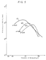
- a so-called slab waveguide-type second harmonic generator was made.
- Fig. 5 shows measured results thereof.
- the second harmonic generator efficiency was measured by the following manner. As shown in Fig.
- a GaP prism 5 was located on the optical waveguide 2, wherein a laser light of wavelength, 1.06 micrometers from the Nd:YAG laser was introduced into the GaP prism 5 and an SHG (second harmonic generation) light 4 emitted from the output end face of the optical waveguide 2 was measured.
- the doped amount of Ti lies in a range of > 0 ⁇ Ti/(Ti + Ta) ⁇ 60 (atomic percents), and more preferably, it lies in a range of 15 ⁇ Ti/(Ti + Ta) ⁇ 60 (atomic percents).
- the optical waveguide 2 made of a TiO2-doped-Ta205 film was formed. In that case, Cerenkov radiation of TE wave mode was observed.
- the optical waveguide 2 made of a TiO2-doped-Ta2O5 film was formed. In that case, Cerenkov radiation of TE wave mode was observed.
- the optical waveguide of the invention is formed as a slab-type optical waveguide, it is possible to form a ridge-type optical waveguide.
- FIG. 7 is an enlarged planar view of the optical waveguide and second harmonic generator according to the present invention
- Fig. 8 is a side view of Fig. 7.
- the optical waveguide 2 was made of the amorphous film in which TiO2 is doped to Ta2O5.
- the direction perpendicular to the longitudinal direction of the optical waveguide 2 was selected to be the z-axis (c-axis) of the substrate 1, and the input end face side of the optical waveguide 2 for the fundamental wave was tapered to be gradually widened toward its end portion 2a.
- a semiconductor laser 6 was optically coupled to the end portion 2a of the optical waveguide 2.
- the X- or Y-cut crystal i.e cut perpendicularly to the z-axis (c-axis) of the LN substrate is employed to effect the TE wave mode, whereby the semiconductor laser can be connected to the optical waveguide as the fundamental wave light source.
- the 1/2 wavelength plate, required by the TM wave mode is not needed.
- an LiNbO3 non-linear single crystal substrate 11 was prepared, and a periodically-poled region 10 was formed on the surface of the substrate 11.
- Arrows a and b in Fig. 11 schematically illustrate directions of periodically-poled regions, respectively.
- the periodically-poled region 10 was formed as follows. Ti-deposited films of striped-shape were deposited on one major surface of, for example, the substrate 11 with predetermined width and pitch in parallel to one another, and were heat-treated at a temperature of 1000°C to 1100°C, for example, 1050°C for several hours, thus the periodically-poled region 10 being made.
- the fundamental waveguide 12 which was manufactured in a three-dimensional manner so as to have a width W of about less than 2 micrometers and a length l of about less than 6 mm.
- the reason that the width W of the fundamental waveguide 12 is selected to be less than 2 micrometers is that this width causes the second harmonic generator to generate an SHG radiation of single mode with ease.
- the reason that the length l is selected to be less than 6 mm is that this length can make the second harmonic generator as small as possible.
- the fundamental waveguide 12 was formed similarly to the example 1.
- the fundamental wavelength was selected to be 0.84 micrometer and a refractive index difference ⁇ n f between the refractive indices of the fundamental waveguide 12 and the LiNbO3 substrate 1 for the fundamental wave was selected to be 0.15 by selecting the TiO2-doped amount of the fundamental waveguide 12. Then, a similar refractive index difference ⁇ n SHG for the wavelength 0.42 micrometer of the secondary harmonic wave generation light was selected to be 0.22.
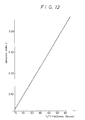
- a relationship between the thickness h of the fundamental waveguide 12 and the periodically-poled region cycle ⁇ (micrometer) for providing an SHG light beam of higher than 10 mW relative to the semiconductor laser light of 100 mW (fundamental wave input) was measured, such relationshiop fell in a hatched range encircled by a solid line 51 in Fig. 13.
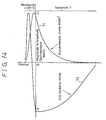
- Fig. 14 illustrates an overlap between the fundamental guide mode and the second harmonic radiation mode according to the present invention under a condition of one point within the range encircled by the solid line 51 in Fig. 13, i.e. under the condition that the thickness h is 0.3 micrometer and the periodically-poled region cycle ⁇ is 3.27 micrometers.
- the second harmonic generator was formed similarly to the example 6 and the thickness h was selected to be 0.80 micrometer and the periodically-poled region cycle ⁇ was selected to be 15 micrometers.
- Fig. 15 shows an overlap between the fundamental guide mode and the second harmonic radiation mode in the case of the comparative example 1.
- the refractive index n of the cladding layer formed on the surface of the fundamental waveguide 12 is selected to be 1.0 (air).
- n f 1.9
- n SHG 2.2
- a range of the thickness h and the periodically-poled region cycle ⁇ (this range will hereinafter be referred to as h - ⁇ range, for simplicity) for presenting the SHG efficiency of more than 10 % in the example 6 falls in a range encircled by a solid line 57 in Fig. 13.
- the wavelength of the semiconductor laser of 0.8 micrometer band i.e.
- the wavelength of the fundamental wave is 0.84 micrometer
- the h - ⁇ range in which the SHG efficiency becomes more than 10 % lies in a region I encircled by a solid line 21 in Fig. 10.
- the wavelength of the semiconductor laser of 0.8 micrometer band is longer than the former, for example, 0.88 micrometer
- the wavelength of the semiconductor laser of 0.8 micrometer band is 0.78 micrometer
- the h - ⁇ range lies in a region III encircled by a solid line 23 in Fig. 10.
- the Cerenkov radiation angle was less than 5 degrees.
- ⁇ n f wavelength of fundamental wave was 0.84 micrometer
- ⁇ n SHG wavelength of SHG wave was 0.42 micrometer
- a second harmonic generator was formed similarly to the example 6, and ⁇ n f was selected to be 0.10, and ⁇ n SHG was selected to be 0.15.
- a second harmonic generator was formed similarly to the example 6, and ⁇ n f was selected to be 0.075, and ⁇ n SHG was selected to be 0.13.
- a second harmonic generator was formed similarly to the example 6, and ⁇ n f was selected to be 0.06 and ⁇ n SHG was selected to be 0.11.
- a second harmonic generator was formed similarly to the example 6, and ⁇ n f was selected to be 0.04 and ⁇ n SHG was selected to be 0.09.
- a second harmonic generator was formed similarly to the example 6, and ⁇ n f was selected to be 0.20 and ⁇ n SHG was selected to be 0.30.
- the range of the thickness h (micrometer) of the fundamental waveguide 12 and the periodically-poled region cycle ⁇ (micrometer) was selected so as to fall within the ranges encircled by the solid lines 52 to 56 in Fig. 13. In that event, the SHG efficiency of more than 10 % could be obtained.
- curves 61 and 71 represent an overlap in the fundamental guide mode
- curves 62 and 72 represent an overlap in the second harmonic radiation mode, respectively.
- the ordinate represents the position of the SHG element 13 in the thickness direction
- a point zero indicates an interface between the fundamental waveguide 12 and the substrate 11.
- One scale corresponds to the thickness of 0.1 micrometer.
- the abscissa represents the magnitude of the amplitude of the electric field. In the fundamental guide mode, the square of the amplitude peak is standardized as "1", and in the second harmonic radiation mode, the amplitude peak is standardized as "1".
- the square of the amplitude of the fundamental guide mode and the amplitude of the second harmonic radiation mode sufficiently overlap each other near the interface between the substrate 11 and the waveguide 12.
- the mutual action is very large so that high SHG efficiency can be obtained.
- the SHG efficiency reaches about 30 %, and accordingly, the length of the mutual action, i.e. the length l of the fundamental waveguide 12 can be reduced and made less than 6 mm as described above.
- the Cerenkov radiation angle is about 1 degrees.
- the Cerenkov radiation angle is about 2 degrees.
- the above-mentioned overlap is not produced near the interface between the substrate 11 and the fundamental waveguide 12, and therefore, the SHG efficiency thereof is as small as about 10 ⁇ 3 %.
Landscapes
- Physics & Mathematics (AREA)
- Nonlinear Science (AREA)
- General Physics & Mathematics (AREA)
- Optics & Photonics (AREA)
- Optical Integrated Circuits (AREA)
Claims (7)
- Moyen de guide d'onde optique comprenant :
un substrat (1 ; 11) ; et
un guide d'onde optique (2 ; 12) formé sur ledit substrat en tant que film mince amorphe comprenant du Ta₂O₅,
caractérisé en ce que ledit film mince amorphe est constitué par un matériau du système Ta₂O₅ - TiO₂ dans lequel la quantité de Ti par rapport à la somme du Ti et du Ta est choisie de manière à s'inscrire dans la plage qui va de 0 à 60 % en pourcentage atomique. - Générateur d'harmonique d'ordre deux du type à rayonnement Cerenkov, comprenant un guide d'onde optique selon la revendication 1, dans lequel ledit substrat est en un matériau optique non linéaire.
- Générateur d'harmonique d'ordre deux selon la revendication 2, dans lequel ledit substrat en matériau optique non linéaire est un monocristal optique non linéaire en coupe Y ou en coupe X, ledit guide d'onde optique présente une face d'extrémité large (2a) qui est couplée optiquement à un laser à semiconducteur (6), et ledit guide d'onde optique présente des flancs évasés de façon à avoir une largeur qui diminue progressivement depuis ladite face d'extrémité large jusqu'à son autre face d'extrémité.
- Générateur d'harmonique d'ordre deux selon la revendication 2, dans lequel ledit substrat en matériau optique non linéaire est un substrat en LiNbO₃.
- Générateur d'harmonique d'ordre deux selon la revendication 2, dans lequel ledit substrat en matériau optique non linéaire (11) se voit former sur l'une de ses surfaces une région polarisée périodiquement (10).
- Générateur d'harmonique d'ordre deux selon la revendication 5, dans lequel la relation qui lie le cycle de région polarisée périodiquement Λ de la région polarisée périodiquement et l'épaisseur h du guide d'onde fondamentale est agencée pour tomber dans une plage qui est formée en reliant successivement selon une ligne rectiligne les points (2,38 ; 0,5), (3,5 ; 0,5), (4,46 : 0,16), (2,38 : 0,16) et (2,38 : 0,5) dans des coordonnées (x, y) d'un système de coordonnées orthogonales dans lequel le cycle de région polarisée périodiquement Λ (micromètre) est représenté sur l'axe des x et l'épaisseur h (micromètre) est représentée sur l'axe des y (figure 10).
- Générateur d'harmonique d'ordre deux selon la revendication 6, dans lequel ledit substrat est un substrat en LiNbO₃.
Applications Claiming Priority (8)
| Application Number | Priority Date | Filing Date | Title |
|---|---|---|---|
| JP63265787A JPH02111925A (ja) | 1988-10-21 | 1988-10-21 | 光第2高調波発生素子 |
| JP265785/88 | 1988-10-21 | ||
| JP265787/88 | 1988-10-21 | ||
| JP26578688A JPH02210333A (ja) | 1988-10-21 | 1988-10-21 | 光第2高調波発生素子 |
| JP26578588A JPH02236506A (ja) | 1988-10-21 | 1988-10-21 | 光導波路装置 |
| JP265786/88 | 1988-10-21 | ||
| JP141946/89 | 1989-06-02 | ||
| JP1141946A JPH036540A (ja) | 1989-06-02 | 1989-06-02 | 光第2高調波発生素子 |
Publications (3)
| Publication Number | Publication Date |
|---|---|
| EP0365039A2 EP0365039A2 (fr) | 1990-04-25 |
| EP0365039A3 EP0365039A3 (en) | 1990-10-17 |
| EP0365039B1 true EP0365039B1 (fr) | 1994-03-30 |
Family
ID=27472415
Family Applications (1)
| Application Number | Title | Priority Date | Filing Date |
|---|---|---|---|
| EP89119535A Expired - Lifetime EP0365039B1 (fr) | 1988-10-21 | 1989-10-20 | Guide d'onde optique et générateur d'harmonique du second ordre |
Country Status (3)
| Country | Link |
|---|---|
| US (1) | US5022729A (fr) |
| EP (1) | EP0365039B1 (fr) |
| DE (1) | DE68914240T2 (fr) |
Cited By (1)
| Publication number | Priority date | Publication date | Assignee | Title |
|---|---|---|---|---|
| DE102005004478A1 (de) * | 2004-09-30 | 2006-04-06 | Osram Opto Semiconductors Gmbh | Trapezlaservorrichtung |
Families Citing this family (26)
| Publication number | Priority date | Publication date | Assignee | Title |
|---|---|---|---|---|
| EP0452828B1 (fr) * | 1990-04-19 | 1995-06-21 | Sony Corporation | Dispositif à guide d'onde optique et deuxième générateur harmonique utilisant ce dispositif |
| US5854870A (en) * | 1990-05-25 | 1998-12-29 | Hitachi, Ltd. | Short-wavelength laser light source |
| US5064265A (en) * | 1990-06-04 | 1991-11-12 | Hoechst Celanese Corp. | Optical parametric amplifier |
| JP2949807B2 (ja) * | 1990-08-24 | 1999-09-20 | ソニー株式会社 | 光導波路装置及びその製造方法 |
| US5058970A (en) * | 1990-09-17 | 1991-10-22 | Eastman Kodak Company | Quasi-phase matching optical waveguide |
| JP2750231B2 (ja) * | 1990-11-05 | 1998-05-13 | 富士通株式会社 | 導波路型第2高調波発生素子の製造方法 |
| JP3052501B2 (ja) * | 1990-11-30 | 2000-06-12 | 松下電器産業株式会社 | 波長変換素子の製造方法 |
| FR2684772B1 (fr) * | 1991-12-10 | 1994-08-26 | Thomson Csf | Reseau d'indice optique commandable electriquement. |
| US5412502A (en) * | 1992-01-24 | 1995-05-02 | Hitachi Metals, Ltd. | Second harmonic generating element and the production method thereof |
| US5185752A (en) * | 1992-02-18 | 1993-02-09 | Spectra Diode Laboratories, Inc. | Coupling arrangements for frequency-doubled diode lasers |
| JP2783047B2 (ja) * | 1992-03-27 | 1998-08-06 | 松下電器産業株式会社 | 光波長変換素子およびそれを用いたレーザ光源 |
| JPH05333395A (ja) * | 1992-04-03 | 1993-12-17 | Fuji Photo Film Co Ltd | 光波長変換装置 |
| US5339190A (en) * | 1992-04-16 | 1994-08-16 | Nippon Steel Corporation | Optical waveguide second harmonic generating element and method of making the same |
| DE69321539T2 (de) * | 1992-08-26 | 1999-05-27 | Sony Corp., Tokio/Tokyo | Optischer Wellenlängenkonverter |
| KR100393179B1 (ko) * | 1995-06-30 | 2003-10-22 | 삼성전자주식회사 | 준위상정합제2고조파발생장치의제조방법 |
| JP3686153B2 (ja) * | 1996-03-08 | 2005-08-24 | 松下電器産業株式会社 | 永久磁石モータの着磁方法 |
| US5898718A (en) * | 1997-05-19 | 1999-04-27 | Altos Inc. | Method and apparatus for optimizing the output of a multi-peaked frequency harmonic generator |
| JP4660999B2 (ja) * | 2001-08-01 | 2011-03-30 | パナソニック株式会社 | 光導波路デバイス及びコヒーレント光源及び光学装置 |
| KR100400547B1 (ko) * | 2001-08-27 | 2003-10-08 | 엘지전자 주식회사 | 1차원 광 모듈레이터 및 이를 이용한 투사장치 |
| KR100400548B1 (ko) * | 2001-08-27 | 2003-10-08 | 엘지전자 주식회사 | 반사형 1차원 광 모듈레이터 및 이를 이용한 투사장치 |
| US6960486B2 (en) * | 2001-09-20 | 2005-11-01 | University Of Alabama At Brimingham Research Foundation | Mid-IR microchip laser: ZnS:Cr2+ laser with saturable absorber material |
| US7405512B2 (en) * | 2006-06-22 | 2008-07-29 | Gooch And Housego Plc | Acoustic transducers having localized ferroelectric domain inverted regions |
| JP2008192829A (ja) * | 2007-02-05 | 2008-08-21 | Univ Waseda | 光増幅器及びその製造方法。 |
| KR101018278B1 (ko) * | 2008-09-19 | 2011-03-04 | 전자부품연구원 | 파장가변 소자 패키지 |
| CN101439968B (zh) * | 2008-12-26 | 2011-07-20 | 北京工业大学 | 一种实现(Ta2O5)1-x(TiO2)x陶瓷介电温度系数热补偿的方法 |
| CN113311636A (zh) * | 2021-05-08 | 2021-08-27 | 南京邮电大学 | 在铌酸锂波导结构中产生二次谐波的方法 |
Family Cites Families (3)
| Publication number | Priority date | Publication date | Assignee | Title |
|---|---|---|---|---|
| US3935472A (en) * | 1975-03-14 | 1976-01-27 | Bell Telephone Laboratories, Incorporated | Thin film liquid waveguide optical converter |
| US4859876A (en) * | 1985-09-16 | 1989-08-22 | AT&T Bell Laboratories American Telephone and Telegraph Company | Nonlinear optical materials and devices |
| US4763019A (en) * | 1986-09-09 | 1988-08-09 | American Telephone And Telegraph Company, At&T Bell Laboratories | Apparatus comprising harmonic generation means |
-
1989
- 1989-10-20 US US07/424,768 patent/US5022729A/en not_active Expired - Fee Related
- 1989-10-20 DE DE68914240T patent/DE68914240T2/de not_active Expired - Fee Related
- 1989-10-20 EP EP89119535A patent/EP0365039B1/fr not_active Expired - Lifetime
Non-Patent Citations (1)
| Title |
|---|
| APPL. OPT. 10, 1037-1042. * |
Cited By (2)
| Publication number | Priority date | Publication date | Assignee | Title |
|---|---|---|---|---|
| DE102005004478A1 (de) * | 2004-09-30 | 2006-04-06 | Osram Opto Semiconductors Gmbh | Trapezlaservorrichtung |
| DE102005004478B4 (de) * | 2004-09-30 | 2009-03-19 | Osram Opto Semiconductors Gmbh | Trapezlaservorrichtung |
Also Published As
| Publication number | Publication date |
|---|---|
| US5022729A (en) | 1991-06-11 |
| EP0365039A3 (en) | 1990-10-17 |
| EP0365039A2 (fr) | 1990-04-25 |
| DE68914240D1 (de) | 1994-05-05 |
| DE68914240T2 (de) | 1994-10-27 |
Similar Documents
| Publication | Publication Date | Title |
|---|---|---|
| EP0365039B1 (fr) | Guide d'onde optique et générateur d'harmonique du second ordre | |
| EP0844511B2 (fr) | Dispositif de conversion de longueur d'onde optique pour la génération du deuxième harmonique | |
| EP0753768B1 (fr) | Dispositif pour changer la longueur d'onde et appareil générateur d'un faisceau laser | |
| US5193023A (en) | Method of controlling the domain of a nonlinear ferroelectric optics substrate | |
| Chen et al. | Guided-wave electro-optic beam deflector using domain reversal in LiTaO/sub 3 | |
| EP0699934A2 (fr) | Procédé de fabrication de domaines inversés et dispositif optique de conversion de longueur d'onde avec ces dernières | |
| EP0485159B1 (fr) | Méthode de fabrication d'un dispositif en guide d'onde pour la génération du deuxième harmonique | |
| US5373575A (en) | Frequency doubler and short wave laser source using the same and optical data processing apparatus using the short wave laser source | |
| EP0463886B1 (fr) | Convertisseur de longueur d'onde optique | |
| EP0452828B1 (fr) | Dispositif à guide d'onde optique et deuxième générateur harmonique utilisant ce dispositif | |
| JP3296500B2 (ja) | 波長変換素子およびその製造方法 | |
| EP0432390B1 (fr) | Dispositif pour générer une onde de seconde harmonique et méthode de production du même | |
| US6204957B1 (en) | Second harmonic wave-generating element | |
| JP2851935B2 (ja) | コリニア型光偏向器及びその製造方法並びに光偏向装置及び光集積ヘッド及び光情報記録再生装置 | |
| JP2973463B2 (ja) | 光導波路装置 | |
| Huang et al. | Study of the optical properties of rf sputtered lithium niobate thin films | |
| JP3086239B2 (ja) | プロトン交換光導波路とその製造方法及びこの導波路を用いた光偏向器 | |
| JPH02189528A (ja) | 導波路型波長変換素子 | |
| JPH02210333A (ja) | 光第2高調波発生素子 | |
| JPH0445430A (ja) | 導波路型波長変換素子 | |
| JPH036540A (ja) | 光第2高調波発生素子 | |
| JPH0534745A (ja) | 光波長変換素子及びその作製方法 | |
| JPH04309931A (ja) | チャンネル導波路型光第2高調波発生装置 | |
| JPH0572589A (ja) | 第2高調波発生素子 | |
| JPH04257829A (ja) | 導波路型shg素子 |
Legal Events
| Date | Code | Title | Description |
|---|---|---|---|
| PUAI | Public reference made under article 153(3) epc to a published international application that has entered the european phase |
Free format text: ORIGINAL CODE: 0009012 |
|
| AK | Designated contracting states |
Kind code of ref document: A2 Designated state(s): DE FR GB |
|
| PUAL | Search report despatched |
Free format text: ORIGINAL CODE: 0009013 |
|
| AK | Designated contracting states |
Kind code of ref document: A3 Designated state(s): DE FR GB |
|
| 17P | Request for examination filed |
Effective date: 19901220 |
|
| 17Q | First examination report despatched |
Effective date: 19921030 |
|
| GRAA | (expected) grant |
Free format text: ORIGINAL CODE: 0009210 |
|
| AK | Designated contracting states |
Kind code of ref document: B1 Designated state(s): DE FR GB |
|
| REF | Corresponds to: |
Ref document number: 68914240 Country of ref document: DE Date of ref document: 19940505 |
|
| ET | Fr: translation filed | ||
| PLBE | No opposition filed within time limit |
Free format text: ORIGINAL CODE: 0009261 |
|
| STAA | Information on the status of an ep patent application or granted ep patent |
Free format text: STATUS: NO OPPOSITION FILED WITHIN TIME LIMIT |
|
| 26N | No opposition filed | ||
| PGFP | Annual fee paid to national office [announced via postgrant information from national office to epo] |
Ref country code: FR Payment date: 20011010 Year of fee payment: 13 |
|
| PGFP | Annual fee paid to national office [announced via postgrant information from national office to epo] |
Ref country code: GB Payment date: 20011024 Year of fee payment: 13 |
|
| PGFP | Annual fee paid to national office [announced via postgrant information from national office to epo] |
Ref country code: DE Payment date: 20011105 Year of fee payment: 13 |
|
| REG | Reference to a national code |
Ref country code: GB Ref legal event code: IF02 |
|
| PG25 | Lapsed in a contracting state [announced via postgrant information from national office to epo] |
Ref country code: GB Free format text: LAPSE BECAUSE OF NON-PAYMENT OF DUE FEES Effective date: 20021020 |
|
| PG25 | Lapsed in a contracting state [announced via postgrant information from national office to epo] |
Ref country code: DE Free format text: LAPSE BECAUSE OF NON-PAYMENT OF DUE FEES Effective date: 20030501 |
|
| GBPC | Gb: european patent ceased through non-payment of renewal fee |
Effective date: 20021020 |
|
| PG25 | Lapsed in a contracting state [announced via postgrant information from national office to epo] |
Ref country code: FR Free format text: LAPSE BECAUSE OF NON-PAYMENT OF DUE FEES Effective date: 20030630 |
|
| REG | Reference to a national code |
Ref country code: FR Ref legal event code: ST |