EP0365095A2 - Ensemble avec une photodiode semi-conducteur à effet d'avalanche et un circuit de quenching actif - Google Patents
Ensemble avec une photodiode semi-conducteur à effet d'avalanche et un circuit de quenching actif Download PDFInfo
- Publication number
- EP0365095A2 EP0365095A2 EP89202618A EP89202618A EP0365095A2 EP 0365095 A2 EP0365095 A2 EP 0365095A2 EP 89202618 A EP89202618 A EP 89202618A EP 89202618 A EP89202618 A EP 89202618A EP 0365095 A2 EP0365095 A2 EP 0365095A2
- Authority
- EP
- European Patent Office
- Prior art keywords
- quenching
- circuit
- photodiode
- comparator
- spad
- Prior art date
- Legal status (The legal status is an assumption and is not a legal conclusion. Google has not performed a legal analysis and makes no representation as to the accuracy of the status listed.)
- Ceased
Links
Images


Classifications
-
- H—ELECTRICITY
- H03—ELECTRONIC CIRCUITRY
- H03K—PULSE TECHNIQUE
- H03K17/00—Electronic switching or gating, i.e. not by contact-making and –breaking
- H03K17/51—Electronic switching or gating, i.e. not by contact-making and –breaking characterised by the components used
- H03K17/74—Electronic switching or gating, i.e. not by contact-making and –breaking characterised by the components used by the use, as active elements, of diodes
-
- G—PHYSICS
- G01—MEASURING; TESTING
- G01J—MEASUREMENT OF INTENSITY, VELOCITY, SPECTRAL CONTENT, POLARISATION, PHASE OR PULSE CHARACTERISTICS OF INFRARED, VISIBLE OR ULTRAVIOLET LIGHT; COLORIMETRY; RADIATION PYROMETRY
- G01J1/00—Photometry, e.g. photographic exposure meter
- G01J1/42—Photometry, e.g. photographic exposure meter using electric radiation detectors
- G01J1/44—Electric circuits
-
- H—ELECTRICITY
- H03—ELECTRONIC CIRCUITRY
- H03K—PULSE TECHNIQUE
- H03K17/00—Electronic switching or gating, i.e. not by contact-making and –breaking
- H03K17/94—Electronic switching or gating, i.e. not by contact-making and –breaking characterised by the way in which the control signals are generated
- H03K17/941—Electronic switching or gating, i.e. not by contact-making and –breaking characterised by the way in which the control signals are generated using an optical detector
-
- G—PHYSICS
- G01—MEASURING; TESTING
- G01J—MEASUREMENT OF INTENSITY, VELOCITY, SPECTRAL CONTENT, POLARISATION, PHASE OR PULSE CHARACTERISTICS OF INFRARED, VISIBLE OR ULTRAVIOLET LIGHT; COLORIMETRY; RADIATION PYROMETRY
- G01J1/00—Photometry, e.g. photographic exposure meter
- G01J1/42—Photometry, e.g. photographic exposure meter using electric radiation detectors
- G01J1/44—Electric circuits
- G01J2001/4446—Type of detector
- G01J2001/446—Photodiode
- G01J2001/4466—Avalanche
Definitions
- This invention relates to an active quenching circuit for single photon semiconductor avalanche photodiodes, that is biased with a reverse voltage higher than the breakdown voltage and operating in a triggered avalanche mode, suitable for operation with a photodiode in a remote position.
- the quenching circuit To operate correctly, the quenching circuit must detect the leading edge of the avalanche current coming from the photodiode and in response to it:
- the active quenching circuits developed so far do not permit to operate the photodiode remote from the circuit and connected to it by a coaxial cable. Furthermore, they accept quenching pulses of just a few volts, and thus permit to bias the photodiode above the breakdown voltage by only these few volts. Lastly, the adjustement of these circuits turns out to be quite critical, as concerns the operating difficulties mentioned above.
- the object of the present invention is to accomplish an active quenching circuit for single photon semiconductor avalanche photodiodes, which can avoid the drawbacks mentioned above.
- the object of the present invention is to accomplish an active quenching circuit which can operate without problems even if the photodiode is in a remote position.
- the object of the present invention is also to accomplish a quenching circuit capable of applying quenching impulses as high as required in order to bias the photodiode well above the breakdown voltage.
- the object of the present invention is to accomplish a fast quenching circuit, well synchronized with the leading edge of the avalanche current, and being easy to adjust.
- the active quenching circuit characterized mainly in that it comprises a signal comparator having a first input connected to the photodiode under control and a second input connected to a balancing impedance equal to that of the photodiode, a generator of the quenching signal connected to the output of said comparator so as to generate a quenching signal of the photodiode having a predetermined duration each time there is an imbalance between two inputs of the comparator and circuit switching means included in a connecting circuit to said photodiode and to said balancing impedance at the inputs of said comparator and at the outputs of said generator and driven by said quenching signal so as to hold normally high the bias voltage of the photodiode and to lower it below the breakdown level for a predetermined time after the generation of said quenching signal.
- the symmetry accomplished at the two comparator inputs achieves the conditioon that the irregularities of the quenching signals and the reflections generated by the photodiode and by the balancing impedance are equal at the two comparator inputs, so as to cancel one another out and avoid the generation of a false quenching signal.
- the avalanche current pulse caused by a photon absorbed by the photodiode is instead applied only at the input connected to the photodiode itself and therefore represents a differential signal, which triggers the quenching circuit.
- the presence of the circuital switches at the inputs of the quenching circuit permits the application to the photodiode of voltage pulses as large as possible, even up to some tens of volts, without being limited by the peak voltage admissible at the quenching circuit inputs.
- such switches contribute to the reduction of the possibility that the quenching circuit may oscillate, since they interrupt a positive feedback loop within the circuit.
- Fig. 1 it is indicated with SPAD a single photon semiconductor avalanche photodiode, which is arranged in a remote position with respect to the quenching circuit and is connected to it by means of a coaxial cable CC1, in series to which there is a termination resistance Ro1.
- the series of the photodiode SPAD, of the coaxial cable CC1 and of the termination resistance Ro1 is connected between one terminal having negative voltage -Vr and a circuital branch point N1, in turn connected to a power supply terminal having positive voltage +V through a resistance R1.
- the quenching circuit for the photodiode SPAD comprises a comparator CP, which has a positive input, a negative input and an output which is activated in case of a difference between the two signals applied across the two inputs.
- a PNP transistor T1, T2 is connected to each of the two inputs, having a common case configuration, that is with the base connected to a low impedance direct power supply and with a signal received by the emitter and delivered by the collector.
- the function of said transistors is to present a low impedance to the current signals and to permit them to develop a voltage at the comparator input across a resistance having a value not restricted to that of the characteristic impedance of the line, and in particular greater than the same.
- the positive input of the comparator CP is connected to the circuit branch point N1, and thus to the photodiode SPAD, through a PNP transistor T1 having the collector connected to the above positive input and to ground through a resistance R2, the base connected to a positive power supply voltage and the emitter connected to a terminal having positive voltage +V through a resistance R3 and to the circuit branch point N1 by means of a normally closed circuital switch I1 constituted, in the example of Fig. 1, by a normally conductive diode D1 held in conduction by the resistance R1 connected to a positive power supply voltage +V.
- the negative input of the comparator CP is in turn connected to a circuital branch point N2 through a PNP transistor T2, identical to T1 and having the same circuital configuration, and a normally closed circuital switch I2, identical to I1, constituted, in the example of Fig. 1, by a diode normally held in conduction by a resistance R4 identical to R2, connected to a terminal having positive voltage +V.
- the branch point N2 is, in addition, connected by a termination resistance Ro2 identical to Ro1, to a coaxial cable CC2 identical to CC1; this cable has at the other end a termination capacitor C connected to ground, which emulates the characteristic impedance of the SPAD photodiode.
- the circuital branch point consisting of Ro2, CC2 and C is thus exactly symmetrical with respect to that consisting of Ro1, CC1 and SPAD.
- the output of the comparator CP is connected to the input of one output stage OS provided with an output terminal U and also to the input of a monostable multivibrator M, whose output is connected to the input of two identical driver circuits DR1 and DR2, whose outputs are connected to the circuital branch points N1 and N2 by respective normally non-conductive diodes D3 and D4, constituting normally open circuital switches I3 and I4.
- the photodiode SPAD is biased at a voltage higher than that of breakdown and the two diodes D1 and D2 are both in conduction, that is the switches I1 and I2 are closed, while neither of the two diodes D3 and D4 conduct, that is the switches I3 and I4 are open.
- a single photon absorbed by the photodiode SPAD is thus capable of causing an avalanche current through the photodiode itself with a consequent decrease of the current through the transistor T1 and the equally consequent application of a negative voltage front across the positive input of the comparator CP.
- the comparator thus detects a differential signal at its inputs and generates at the output a negative front which produces an output at the terminal U and drives the monostable multivibrator M to generate a quenching pulse S having a predetermined duration.
- the negative front of the quenching pulse through the two drives circuits DR1 and DR2, causes the conduction of the diodes D3 and D4 (that is, the closing of the switches I3 and I4) and the cut-off of the diodes D1 and D2 (that is, the opening of the switches I1 and I2) with the consequent application of equal negative voltage fronts across the inputs of the comparator CP, whose output returns with a positive front to the initial level.
- the quenching signal applied to the photodiode lasts for the time set by the monostable multivibrator M, during which the photodiode SPAD is held in a hold-off condition.
- the positive front of the quenching signal returns the diodes D3 and D4 to a cut-off consition (that is, it reopens the switches I3 and I4) and returns the diodes D1 and D2 to conduction (that is, it recloses the switches I2 and I2) and causes the bias voltage of the photodiode SPAD to rise above the breakdown voltage, setting the photodiode itself ready for a new operational cycle. Since the variations detected at the inputs of the comparator CP are identical, the latter's output is unchanged.
- driver circuits DRI and DR2 must be designed as low impedance drivers, so as to be able to drive the considerable voltage excursions required across essentially capacitative loads, such as the photodiode SPAD and the corresponding termination C.
- the generation of the quenching signal causes the application of identical voltage fronts across the two inputs of the comparator CP.
- This is due to the perfect symmetry of the branch Ro2, CC2 and C with respect to the one Ro1, CC1 and SPAD which includes the photodiode, and to the symmetry of the two driver circuits DR1 and DR2.
- possible irregularities of the quenching signal and the reflections on the coaxial cables translate into equal effects across the two inputs of the comparator CP, where they cancel each other out, without determining undesirable triggerings of the quenching circuit.
- the switches I1, I2, I3 and I4 further reduce the possibility of oscillation of the circuit since they interrupt the feedback loop. Moreover, they cause the entire avalanche current to flow through the circuit input, avoiding that part of it be diverted to the output of the quenching driver.
- the switches I1, I2, I3, I4 may be implemented with simple fast-switching diodes, but they may be implemented also with other devices such as field effect transistors with junction structure JFET or with MOS structure MOSFET. Moreover, in those cases where it is sufficient to have a quenching signal with amplitude lower than the breakdown voltage of the emitter-base junction of the PNP transistors N1 and N2, which typically is about 5 volts, the switches I1 and I2 may be constituted by such emitter-base junctions of T1 and T2, avoiding the interposition of the diodes D1 and D2.
- Fig. 2 shows a variant of the quenching circuit according to the invention, which differs from the embodiment exemplified in Fig. 1, in that the circuit inputs have a high impedance and as a consequence the termination resistances Ro1 and Ro2 are connected in parallel to such inputs and placed after the switches I1 and I2 rather than before them.
- switches I2 and I2 are again illustrated as being constituted by diodes D1 and D2, but they still can be implemented with other electronic components, such as JFET and MOSFET.
- the photodiode SPAD may be not in a remote position.
- the circuits of Fig. 1 and Fig. 2 will evidently not include the coaxial cables CC1 and CC2 and, as a consequence, the resistances Ro1 and Ro2 will no longer be restricted to the value of the cable characteristic impedance.
- Fig. 3 shows a variant of interest in the use of photodiodes requiring very high quenching signals, greater than 10 volts, located far from the quenching circuit.
- the capacitance of the coaxial cable (several hundred pF's) is driven by logic voltage pulses having a small amplitude (typically of the order of half a volt), while the large quenching signal (tens of volts) is applied only to the capacitance associated with the photodiode (of the order of a few pF's).
- Fig. 3 the part of the circuit to be mounted on the small circuit board is enclosed within a heavy dash-and dot line and indicated with P.
- the two resistances Ro3 and Ro4 must still be symmetrical, of equal value, but they do not have to provide any more a matched termination to the cables CC1 and CC2, from which they are in any case separated by an open switch.
- the value of Ro3 and Ro4 is not restricted to that of the cable characteristic impedance.
- the cable CC3 may be terminated on its characteristic resistance at the output from the monostable multivibrator block M. As an alternative, or in addition, it can be terminated at the other extremity, connected to the branch point N3 of the common input of the two driver circuits DR1 and DR2, connecting between said branch point N3 and ground a resistance Ro5 having a value equal to that of the characteristic impedance of the cable, that is typically 50 Ohms.
- the recovey of the bias voltage at the end of the hold-off time is fast, but has a finite, non negligible duration. This duration depends on the capacitance to be charged (and therefore on the length of the cables) and on the detailed implementation of the active quenching circuit. It may take from some nanoseconds to some hundred nanoseconds in practical cases.
- the electrical output pulse is not correctly related to the true arrival time. Since the SPAD is triggered when the bias voltage is lower than the normal operating level, the rise of the avalanche current is slower and attains a smaller current value. Compared to the operation in normal conditions, the electrical output pulse has therefore a longer delay, referred to the photon arrival time.
- the resulting problem is that at high repetition rate of the SPAD pulses, a significant percentage of the photons is not correctly timed, that is they generate electrical pulses with randomly incremented delay. This fact causes a degradation of the time resolution obtained in time-correlated single-photon counting.
- the above mentioned degradation of the resolution can be avoided by complementing the active-quenching circuit with an auxiliary circuit.
- the task of this circuit is to recognize and reject the pulses corresponding to photons arriving during the recovery of the bias voltage.
- a rectangular pulse is generated, with a duration sufficient to cover the complete voltage recovery, or somewhat longer.
- This rectangular pulse is used to inhibit output pulses corresponding to SPAD triggering events that occur within the duration of said pulse. This inhibition can be obtained with various types of circuitry.
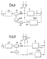
- Two possible schemes of the auxiliary circuit are shown in Figs 4 and 5.
- the output pulse from the comparator CP is applied to an input of a coincidence (AND) circuit CO and, through an interposed delay line DL, to the input of a gate circuit GC.
- the other input of the coincidence circuit CO receives a rectangular pulse RP generated by a recovery marker generator RMG.
- the gate GC is controlled through a monostable multivibrator MM by the coincidence output and is normally open.
- the output stage OS of the active quenching circuit receives the output pulse of the said gate.
- an AND output pulse is generated which closes the gate circuit GC for a time sufficient to inhibit the CP output pulse from reaching the output stage OS.
- the rectangular pulse RP generated by RMC is applied to a latch input LI of the comparator CP of the active quenching circuit.
- the comparator CP is therefore latched to its quiescent state; if the SPAD current is triggered within the time interval marked by the said rectangular pulse, the comparator CP will not respond until the said rectangular pulse ends. It may be observed that the SPAD current will not be quenched; it will persist until the said rectangular pulse ends and at this time it will trigger the comparator CP and initiate a quenching cycle. However, it is very easy to inhibit the corresponding pulse to reach the output, since it is synchronized to the trailing edge of the rectangular latching pulse.
- a normally open gate circuit GC is interposed before the output stage OS. In correspondence to the trailing edge of the latching pulse, a pulse with suitable duration is generated by a monostable multivibrator MM and closes the gate GC.
- pulsed driversDR1 and DR2 are:
Landscapes
- Physics & Mathematics (AREA)
- General Physics & Mathematics (AREA)
- Spectroscopy & Molecular Physics (AREA)
- Light Receiving Elements (AREA)
- Photometry And Measurement Of Optical Pulse Characteristics (AREA)
- Electronic Switches (AREA)
Applications Claiming Priority (2)
| Application Number | Priority Date | Filing Date | Title |
|---|---|---|---|
| IT2236788 | 1988-10-20 | ||
| IT8822367A IT1229945B (it) | 1988-10-20 | 1988-10-20 | Circuito di spegnimento attivo per fotodiodi a semiconduttore a valanga per singoli fotoni, adatto per il funzionamento con fotodiodo in posizione remota |
Publications (2)
| Publication Number | Publication Date |
|---|---|
| EP0365095A2 true EP0365095A2 (fr) | 1990-04-25 |
| EP0365095A3 EP0365095A3 (fr) | 1991-02-06 |
Family
ID=11195308
Family Applications (1)
| Application Number | Title | Priority Date | Filing Date |
|---|---|---|---|
| EP19890202618 Ceased EP0365095A3 (fr) | 1988-10-20 | 1989-10-17 | Ensemble avec une photodiode semi-conducteur à effet d'avalanche et un circuit de quenching actif |
Country Status (4)
| Country | Link |
|---|---|
| US (1) | US4963727A (fr) |
| EP (1) | EP0365095A3 (fr) |
| JP (1) | JPH02170477A (fr) |
| IT (1) | IT1229945B (fr) |
Cited By (4)
| Publication number | Priority date | Publication date | Assignee | Title |
|---|---|---|---|---|
| WO1991000502A1 (fr) * | 1989-07-03 | 1991-01-10 | The Secretary Of State For Defence In Her Britannic Majesty's Government Of The United Kingdom Of Great Britain And Northern Ireland | Circuit d'extinction pour photodiodes a avalanche |
| US5933042A (en) * | 1997-07-01 | 1999-08-03 | Eg&G Canada, Ltd. | Active quench circuit for an avalanche current device |
| WO2000038248A1 (fr) * | 1998-12-18 | 2000-06-29 | The Secretary Of State For Defence | Ameliorations apportees a des photodiodes a avalanche |
| US9671284B1 (en) | 2016-01-14 | 2017-06-06 | Kiskeya Microsystems Llc | Single-photon avalanche diode circuit with variable hold-off time and dual delay regime |
Families Citing this family (59)
| Publication number | Priority date | Publication date | Assignee | Title |
|---|---|---|---|---|
| GB8906650D0 (en) * | 1989-03-22 | 1989-05-04 | Harley Phillip E | Electronic quenching circuit |
| US5198701A (en) * | 1990-12-24 | 1993-03-30 | Davies Robert B | Current source with adjustable temperature variation |
| US5526546A (en) * | 1993-04-23 | 1996-06-18 | Revlon Consumer Products Corporation | Surface treated applicators having bristles coated with an etched layer ions produced by an ion-producing gas plasma |
| US5521743A (en) * | 1993-12-16 | 1996-05-28 | Rockwell International Corporation | Photon-counting spatial light modulator with APD structure |
| US5532474A (en) * | 1993-12-17 | 1996-07-02 | Eg&G Limited | Active quench circuit and reset circuit for avalanche photodiode |
| US6218657B1 (en) * | 1998-10-15 | 2001-04-17 | International Business Machines Corporation | System for gated detection of optical pulses containing a small number of photons using an avalanche photodiode |
| US6580845B1 (en) | 2000-08-11 | 2003-06-17 | General Nutronics, Inc. | Method and device for switching wavelength division multiplexed optical signals using emitter arrays |
| US6696887B2 (en) * | 2001-09-27 | 2004-02-24 | Matthew S. Taubman | Transistor-based interface circuitry |
| CN100410636C (zh) * | 2004-03-19 | 2008-08-13 | 华东师范大学 | 一种apd单光子探测的电路模块 |
| US7045761B2 (en) * | 2004-06-21 | 2006-05-16 | The Boeing Company | Self-pixelating focal plane array with electronic output |
| DE102005051571B4 (de) * | 2005-10-21 | 2013-06-20 | Fraunhofer-Gesellschaft zur Förderung der angewandten Forschung e.V. | Photodioden-Chip hoher Grenzfrequenz |
| US7897906B2 (en) * | 2007-03-23 | 2011-03-01 | Excelitas Canada Inc. | Double quench circuit for an avalanche current device |
| CN101170362B (zh) * | 2007-11-08 | 2011-01-12 | 华东师范大学 | 一种apd单光子探测的电路模块 |
| US8803075B2 (en) * | 2008-04-18 | 2014-08-12 | Saint-Gobain Ceramics & Plastics, Inc. | Radiation detector device |
| CN101923173B (zh) * | 2009-06-10 | 2014-10-01 | 圣戈本陶瓷及塑料股份有限公司 | 闪烁体以及检测器组件 |
| US9354113B1 (en) | 2010-11-05 | 2016-05-31 | Stc.Unm | Impact ionization devices under dynamic electric fields |
| DE102010060527B3 (de) * | 2010-11-12 | 2012-04-19 | Picoquant Gmbh | Schaltungsanordnung zum Nachweis einzelner Photonen |
| US9442201B2 (en) | 2013-09-12 | 2016-09-13 | Siemens Medical Solutions Usa, Inc. | CMOS SPAD array with mixed timing pick-off for time-of-flight positron emission tomography |
| US10128398B1 (en) | 2014-05-23 | 2018-11-13 | Stc.Unm | Resonance avalanche photodiodes for dynamic biasing |
| CN104218917A (zh) * | 2014-07-24 | 2014-12-17 | 安徽问天量子科技股份有限公司 | 用于消除apd雪崩信号输出端的尖峰噪声的自差分滤波装置 |
| CN104198058B (zh) * | 2014-08-05 | 2017-06-06 | 清华大学 | 单光子雪崩二极管的淬灭和读出电路 |
| CN104990632A (zh) * | 2015-07-14 | 2015-10-21 | 华中科技大学 | 一种门控差分单光子探测系统 |
| CN106482840B (zh) * | 2016-09-27 | 2019-03-08 | 山东大学 | 一种用于单光子探测器的主动猝灭电路及其工作方法 |
| US10340408B1 (en) | 2018-05-17 | 2019-07-02 | Hi Llc | Non-invasive wearable brain interface systems including a headgear and a plurality of self-contained photodetector units configured to removably attach to the headgear |
| US10515993B2 (en) | 2018-05-17 | 2019-12-24 | Hi Llc | Stacked photodetector assemblies |
| US10158038B1 (en) | 2018-05-17 | 2018-12-18 | Hi Llc | Fast-gated photodetector architectures comprising dual voltage sources with a switch configuration |
| US10420498B1 (en) | 2018-06-20 | 2019-09-24 | Hi Llc | Spatial and temporal-based diffusive correlation spectroscopy systems and methods |
| US11213206B2 (en) | 2018-07-17 | 2022-01-04 | Hi Llc | Non-invasive measurement systems with single-photon counting camera |
| WO2020131148A1 (fr) | 2018-12-21 | 2020-06-25 | Hi Llc | Rétroaction biologique pour la perception et la modulation de l'état mental à l'aide d'un système et d'un procédé non invasifs d'interface cérébrale |
| JP7278821B2 (ja) | 2019-03-22 | 2023-05-22 | 株式会社東芝 | センサ及び距離計測装置 |
| WO2020226840A1 (fr) | 2019-05-06 | 2020-11-12 | Hi Llc | Architectures de photodétecteur pour comptage de photons uniques corrélé dans le temps |
| WO2020236371A1 (fr) | 2019-05-21 | 2020-11-26 | Hi Llc | Architectures de photodétecteur pour déclenchement rapide efficace |
| US10868207B1 (en) | 2019-06-06 | 2020-12-15 | Hi Llc | Photodetector systems with low-power time-to-digital converter architectures to determine an arrival time of photon at a photodetector based on event detection time window |
| US11105679B2 (en) | 2019-12-12 | 2021-08-31 | Stmicroelectronics (Research & Development) Limited | Extended hold-off time for SPAD quench assistance |
| US11162839B2 (en) * | 2019-12-12 | 2021-11-02 | Stmicroelectronics (Research & Development) Limited | Photodetection circuit with extended hold-off time for SPAD quench assistance |
| US11883181B2 (en) | 2020-02-21 | 2024-01-30 | Hi Llc | Multimodal wearable measurement systems and methods |
| WO2021167876A1 (fr) | 2020-02-21 | 2021-08-26 | Hi Llc | Procédés et systèmes permettant d'initier et de mener une étude personnalisée de recherche cérébrale activée par ordinateur |
| US11096620B1 (en) | 2020-02-21 | 2021-08-24 | Hi Llc | Wearable module assemblies for an optical measurement system |
| US11969259B2 (en) | 2020-02-21 | 2024-04-30 | Hi Llc | Detector assemblies for a wearable module of an optical measurement system and including spring-loaded light-receiving members |
| WO2021167892A1 (fr) | 2020-02-21 | 2021-08-26 | Hi Llc | Dispositifs et ensembles portables avec positionnement réglable destinés à être utilisés dans un système de mesure optique |
| US12029558B2 (en) | 2020-02-21 | 2024-07-09 | Hi Llc | Time domain-based optical measurement systems and methods configured to measure absolute properties of tissue |
| US12144653B2 (en) | 2020-02-21 | 2024-11-19 | Hi Llc | Systems, circuits, and methods for reducing common-mode noise in biopotential recordings |
| US11950879B2 (en) | 2020-02-21 | 2024-04-09 | Hi Llc | Estimation of source-detector separation in an optical measurement system |
| WO2021167893A1 (fr) | 2020-02-21 | 2021-08-26 | Hi Llc | Ensembles détecteurs intégrés pour un module pouvant être porté d'un système de mesure optique |
| US11857348B2 (en) | 2020-03-20 | 2024-01-02 | Hi Llc | Techniques for determining a timing uncertainty of a component of an optical measurement system |
| US12085789B2 (en) | 2020-03-20 | 2024-09-10 | Hi Llc | Bias voltage generation in an optical measurement system |
| US11187575B2 (en) | 2020-03-20 | 2021-11-30 | Hi Llc | High density optical measurement systems with minimal number of light sources |
| US12138068B2 (en) | 2020-03-20 | 2024-11-12 | Hi Llc | Techniques for characterizing a nonlinearity of a time-to-digital converter in an optical measurement system |
| WO2021188486A1 (fr) | 2020-03-20 | 2021-09-23 | Hi Llc | Réglage basé sur un circuit en boucle à verrouillage de phase d'une fenêtre de temps de mesure dans un système de mesure optique |
| US12059262B2 (en) | 2020-03-20 | 2024-08-13 | Hi Llc | Maintaining consistent photodetector sensitivity in an optical measurement system |
| US11607132B2 (en) | 2020-03-20 | 2023-03-21 | Hi Llc | Temporal resolution control for temporal point spread function generation in an optical measurement system |
| US11903676B2 (en) | 2020-03-20 | 2024-02-20 | Hi Llc | Photodetector calibration of an optical measurement system |
| US11245404B2 (en) | 2020-03-20 | 2022-02-08 | Hi Llc | Phase lock loop circuit based signal generation in an optical measurement system |
| US11864867B2 (en) | 2020-03-20 | 2024-01-09 | Hi Llc | Control circuit for a light source in an optical measurement system by applying voltage with a first polarity to start an emission of a light pulse and applying voltage with a second polarity to stop the emission of the light pulse |
| WO2021188485A1 (fr) | 2020-03-20 | 2021-09-23 | Hi Llc | Maintien de sensibilité de photodétecteur constante dans un système de mesure optique |
| US11877825B2 (en) | 2020-03-20 | 2024-01-23 | Hi Llc | Device enumeration in an optical measurement system |
| US12059270B2 (en) | 2020-04-24 | 2024-08-13 | Hi Llc | Systems and methods for noise removal in an optical measurement system |
| CN112444315A (zh) * | 2020-10-15 | 2021-03-05 | 良业科技集团股份有限公司 | 一种被动淬灭电路 |
| CN113253088B (zh) * | 2021-06-25 | 2021-09-28 | 上海瞻芯电子科技有限公司 | 晶体管栅氧测试装置及系统 |
Family Cites Families (7)
| Publication number | Priority date | Publication date | Assignee | Title |
|---|---|---|---|---|
| US4001614A (en) * | 1975-08-27 | 1977-01-04 | Hughes Aircraft Company | Bias circuit for a photo-avalanche diode |
| US4303861A (en) * | 1980-03-28 | 1981-12-01 | Battelle Development Corporation | Photon detector system |
| US4389695A (en) * | 1981-02-09 | 1983-06-21 | Carpenter Jr Roy B | Equipment for protecting electronic equipment and personnel against inadvertent occurrence of extended or transient high voltages and method |
| JPS5838041A (ja) * | 1981-08-31 | 1983-03-05 | Asahi Optical Co Ltd | Apdバイアス回路 |
| JPS6278886A (ja) * | 1985-10-01 | 1987-04-11 | Iwatsu Electric Co Ltd | アバランシエ・ホトダイオ−ドのバイアス回路 |
| US4754131A (en) * | 1985-12-31 | 1988-06-28 | American Telephone And Telegraph Company, At&T Bell Laboratories | Devices using avalanche photodiode and capable of detecting a small number of photons |
| DE3780647T2 (de) * | 1986-11-25 | 1993-03-11 | Secr Defence Brit | Quench-schaltung fuer avalanche-photodioden. |
-
1988
- 1988-10-20 IT IT8822367A patent/IT1229945B/it active
-
1989
- 1989-10-17 EP EP19890202618 patent/EP0365095A3/fr not_active Ceased
- 1989-10-18 US US07/422,899 patent/US4963727A/en not_active Expired - Fee Related
- 1989-10-20 JP JP1271887A patent/JPH02170477A/ja active Pending
Cited By (7)
| Publication number | Priority date | Publication date | Assignee | Title |
|---|---|---|---|---|
| WO1991000502A1 (fr) * | 1989-07-03 | 1991-01-10 | The Secretary Of State For Defence In Her Britannic Majesty's Government Of The United Kingdom Of Great Britain And Northern Ireland | Circuit d'extinction pour photodiodes a avalanche |
| US5194727A (en) * | 1989-07-03 | 1993-03-16 | The Secretary Of State For Defence In Her Britannic Majesty's Government Of The United Kingdom Of Great Britain And Northern Ireland | Avalanche photodiode quenching circuit wtih resetting means having a second amplifier |
| US5933042A (en) * | 1997-07-01 | 1999-08-03 | Eg&G Canada, Ltd. | Active quench circuit for an avalanche current device |
| WO2000038248A1 (fr) * | 1998-12-18 | 2000-06-29 | The Secretary Of State For Defence | Ameliorations apportees a des photodiodes a avalanche |
| US6683294B1 (en) | 1998-12-18 | 2004-01-27 | Qinetiq Limited | Avalanche photo-diodes |
| US9671284B1 (en) | 2016-01-14 | 2017-06-06 | Kiskeya Microsystems Llc | Single-photon avalanche diode circuit with variable hold-off time and dual delay regime |
| US10594306B2 (en) | 2016-01-14 | 2020-03-17 | Kiskeya Microsystems Llc | Delay circuit with dual delay resolution regime |
Also Published As
| Publication number | Publication date |
|---|---|
| US4963727A (en) | 1990-10-16 |
| EP0365095A3 (fr) | 1991-02-06 |
| IT8822367A0 (it) | 1988-10-20 |
| JPH02170477A (ja) | 1990-07-02 |
| IT1229945B (it) | 1991-09-17 |
Similar Documents
| Publication | Publication Date | Title |
|---|---|---|
| US4963727A (en) | Active quenching circuit for avalanche photodiodes | |
| US4777387A (en) | Fast turn-off circuit for photovoltaic driven MOSFET | |
| US4885486A (en) | Darlington amplifier with high speed turnoff | |
| US5281925A (en) | RF amplifier providing reduced drive response rise times and fall times | |
| JPH05308717A (ja) | 短絡保護回路 | |
| US3444394A (en) | Ramp-type waveform generator | |
| EP0534680B1 (fr) | Circuit excitateur à diode pin avec étage de tension continue et avec circuit de délai, pour la protection d'un amplificateur bas-bruit de radar contre des signaux HF à haute puissance | |
| US3558917A (en) | Threshold amplitude detector eliminating low-level noise employing threshold-biased interruptable feedback for providing limited range high-gain amplifier operation | |
| US3299288A (en) | Circuits for delaying electric signals with controlled clamps initiating delay | |
| US3983422A (en) | Detector having a constant false alarm rate | |
| US3189844A (en) | Search sweep oscillator comprising one or more three electrode transistors and a double base diode | |
| US5214315A (en) | Nanosecond RF switch driver | |
| US5594256A (en) | High voltage switch for pockels cells | |
| US3459969A (en) | System for producing equal and opposite pulses on selected channels | |
| US3191065A (en) | Sampling circuit | |
| US3581117A (en) | Thyristor circuit having improved turnoff characteristics | |
| US3354323A (en) | Pulse generator with direct connection to output pulse former and time delay in branch circuit | |
| US3965420A (en) | Apparatus for non-destructively testing the voltage characteristics of a transistor | |
| US3596109A (en) | Peak detection circuit | |
| CN116937944A (zh) | 功率器件的门极驱动电路、驱动装置及控制方法 | |
| US4017743A (en) | Elimination of crosstalk in two sequentially operated Darlington amplifier channels | |
| US3422285A (en) | Pulse peak time detecting circuit | |
| SU708502A1 (ru) | Широкополосный амплитудный дискриминатор | |
| US3473044A (en) | Monostable comparator circuit | |
| US3171036A (en) | Flip-flop circuit with single negative resistance device |
Legal Events
| Date | Code | Title | Description |
|---|---|---|---|
| PUAI | Public reference made under article 153(3) epc to a published international application that has entered the european phase |
Free format text: ORIGINAL CODE: 0009012 |
|
| AK | Designated contracting states |
Kind code of ref document: A2 Designated state(s): AT BE CH DE ES FR GB GR IT LI LU NL SE |
|
| PUAL | Search report despatched |
Free format text: ORIGINAL CODE: 0009013 |
|
| AK | Designated contracting states |
Kind code of ref document: A3 Designated state(s): AT BE CH DE ES FR GB GR IT LI LU NL SE |
|
| 17P | Request for examination filed |
Effective date: 19910502 |
|
| 17Q | First examination report despatched |
Effective date: 19930618 |
|
| STAA | Information on the status of an ep patent application or granted ep patent |
Free format text: STATUS: THE APPLICATION HAS BEEN REFUSED |
|
| 18R | Application refused |
Effective date: 19940904 |