EP0366083B1 - Integrierte Schaltung mit Ausgangsschaltung - Google Patents
Integrierte Schaltung mit Ausgangsschaltung Download PDFInfo
- Publication number
- EP0366083B1 EP0366083B1 EP89119746A EP89119746A EP0366083B1 EP 0366083 B1 EP0366083 B1 EP 0366083B1 EP 89119746 A EP89119746 A EP 89119746A EP 89119746 A EP89119746 A EP 89119746A EP 0366083 B1 EP0366083 B1 EP 0366083B1
- Authority
- EP
- European Patent Office
- Prior art keywords
- logic
- voltage
- output
- integrated circuit
- output terminal
- Prior art date
- Legal status (The legal status is an assumption and is not a legal conclusion. Google has not performed a legal analysis and makes no representation as to the accuracy of the status listed.)
- Expired - Lifetime
Links
Images


Classifications
-
- H—ELECTRICITY
- H03—ELECTRONIC CIRCUITRY
- H03K—PULSE TECHNIQUE
- H03K19/00—Logic circuits, i.e. having at least two inputs acting on one output; Inverting circuits
- H03K19/003—Modifications for increasing the reliability for protection
- H03K19/00307—Modifications for increasing the reliability for protection in bipolar transistor circuits
-
- H—ELECTRICITY
- H03—ELECTRONIC CIRCUITRY
- H03K—PULSE TECHNIQUE
- H03K17/00—Electronic switching or gating, i.e. not by contact-making and –breaking
- H03K17/08—Modifications for protecting switching circuit against overcurrent or overvoltage
- H03K17/082—Modifications for protecting switching circuit against overcurrent or overvoltage by feedback from the output to the control circuit
- H03K17/0826—Modifications for protecting switching circuit against overcurrent or overvoltage by feedback from the output to the control circuit in bipolar transistor switches
Definitions
- the present invention generally relates to an integrated circuit having an output circuit, and more particularly to an integrated circuit having an output circuit which is coupled to a bus or a transmission line.
- US-PS 4,384,219 discloses a voltage comparator including a hysteresis control circuit which utilizes a level threshold device.
- the comparator has a first input coupled to an unknown voltage and a second input coupled to a threshold voltage.
- the hysteresis control circuit includes means for generating a hysteresis current which is caused to flow through a hysteresis resistor coupled to the second input when the threshold voltage exceeds the threshold of the level threshold device and the unknown voltage is greater than the voltage on the second input of the comparator.
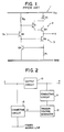
- FIG.1 is a circuit diagram of a conventional output circuit which serves as a bus transmitter.
- an output circuit 1 is made up of transistors Q1 - Q5, a diode (Schottky diode) D1, and resistors R1 and R2.
- Each of the transistors Q1, Q3 and Q4 includes a Schottky diode.
- the transistors Q1 and Q2 and the diode D1 form a first switching circuit 2.
- a second switching circuit 3 includes the transistor Q3.
- a binary logic signal S1 supplied from an input circuit or an internal circuit (not shown) of a device related to the output circuit 1 is applied to the base of the transistor Q4.
- the transistor Q4 turns ON either the first switching circuit 2 or the second switching circuit 3.
- the level of an output terminal X is set approximately equal to a power source voltage Vcc.
- the level of the output terminal X is set approximately equal to a ground potential (GND).
- the resistor R1 generates a voltage proportional to an emitter current passing through the transistor Q3. The generated voltage is applied to the base of the transistor Q5 and causes the base voltage of the transistor Q5 to increase. Accordingly, the emitter current of the transistor Q3 decreases as an increase of the base voltage of the transistor Q5.
- the transistor Q4 turns OFF, and the transistors Q1 and Q2 of the first switching circuit 2 turn ON.
- the logic of the output terminal X is set to logic "1" (equal to Vcc - 2V BE ).
- the transistor Q4 turns ON and the transistor Q3 of the second switching circuit 3 turns ON.
- the logic of the output terminal X is set to logic "0" (approximately equal to the ground potential).
- the resisting voltage of the output circuit 1 viewed from the output terminal X is based on characteristics of the transistors Q1 - Q5. Particularly, the resisting voltage of the output circuit is mainly based on the reverse emitter-base breakdown voltage BV EBO of each of the transistors Q1 and Q2 when the logic of the output terminal X is "0". For this reason, the conventional output circuit does not satisfy the maximum rating defined by a standard such as RS485 in the EIA (Electronic Industries Association) standard.
- the above-mentioned RS485 standard is frequently applied to a bus receiver and a bus transmitter which hold a bidirectional bus in common.
- the recommended operating condition of the RS485 standard is equal to or less than 12 volts.
- the maximum rating which is generally applied to integrated circuits in conformity with the RS485 standard is equal to or less than 15 volts.
- Output resisting (breakdown) voltages BV OH and BV OL for logics H and L are described by the following formulas (1) and (2), respectively: where V BE5 is the forward base-emitter voltage of the transistor Q5, V BE3 is the forward base-emitter voltage of the transistor Q3, V CE4 is the forward collector-emitter saturation voltage of the transistor Q4, the BV EBO1 is the reverse emitter-base breakdown voltage of the transistor Q1, BV EB02 and is the reverse emitter-base breakdown voltage of the transistor Q2.
- the output resisting voltage BV OH 16 volts sufficiently satisfies the maximum rating equal to 15 volts.
- the output resisting voltage BV OL equal to 13 volts does not satisfy the maximum rating. Therefore, when an overvoltage in excess of the recommended operating condition under the maximum rating is applied to the output terminal X from the outside of the output circuit 1 in the state where the output logic of the output circuit 1 is "0", the transistors Q1 and Q2 may be broken down. In order to get rid of this possibility, it is conceivable to deep base diffusion for the transistors Q1 and Q2 so that the voltages BV EBO1 and BV EB02 can be increased so as to satisfy the RS485 standard. However, such an idea presents another disadvantage in that signal transmission becomes slow as the base diffusion is deepened.
- a general object of the present invention is to provide a novel and useful integrated circuit having an output circuit in which the aforementioned disadvantages are eliminated.
- a more specific object of the present invention is to provide an integrated circuit having an output circuit which satisfies a maximum rating which is generally applied to integrated circuits in conformity with the RS485 standard.
- an integrated circuit having an output circuit, a conducting circuit, a trigger voltage generator and a connecting circuit.
- the output circuit has an input terminal and an output terminal and sets the output terminal to a high potential corresponding to logic "1" when the potential applied to the input terminal corresponds to logic "0".
- the output circuit sets the output terminal to a low potential corresponding to logic "0".
- the conducting circuit conducts and passes a current from the output circuit when the potential of the output terminal becomes equal to a predetermined potential higher than the high potential.
- the trigger voltage generator generates a trigger voltage proportional to the current passing through the conducting circuit when it conducts.
- the connecting circuit sets the potential of the input terminal of the output circuit to the low level corresponding to logic "0" when the trigger voltage is applied to the connecting circuit.
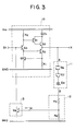
- an output circuit 10 sets an output terminal X to be a high potential corresponding to logic "1" when the potential of an input terminal I corresponds to logic "0".
- the output circuit 10 sets the output terminal X to be a low potential corresponding to logic "0".
- a conducting circuit 11 conducts when the potential of the output terminal X becomes equal to a predetermined high voltage higher than the aforementioned high potential.
- a trigger voltage generator 12 is connected to the output terminal X through a conducting circuit and generates a trigger voltage V T proportional to the predetermined high voltage (or a current passing therethrough) when the conducting circuit 11 conducts.
- a connecting circuit 13 connects the input terminal I to a power source line of a potential corresponding to logic "0" when the trigger voltage V T is applied to the connecting circuit 13.
- the logic of the output terminal X is intentionally set to "1".
- the resisting voltage of the output circuit 10 is increased from BV OL to BV OH .
- the present output circuit can satisfy the specification of the RS485 standard (the maximum rating is equal to or less than 15 volts). It is noted that the logic of the output terminal X is not ensured when it is intentionally set to "1". However, in this case, it is sufficient to protect the output circuit from breakdown due to an overvoltage.
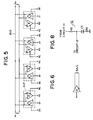
- FIG.3 A description is given of a preferred embodiment of the present invention with reference to FIG.3, in which those parts which are the same as those in FIG.2 are given the same reference numerals.
- the output circuit 10 is of the same structure as the output circuit shown in FIG.1. That is, the output circuit 10 includes the transistors Q1 - Q5, diode D1, and resistors R1 and R2.
- the conducting circuit 11 having an end A connected to the output terminal X, and an end B coupled to ground through the trigger voltage generator 12.
- the conducting circuit 11 is made up of transistors Q6, Q7 and a Schottky diode D2 which are connected in series between the ends A and B.
- the collector and emitter of each of the transistors Q6 and Q7 are mutually connected.
- the base of the transistor Q6 is connected to the emitter and collector of the transistor Q7.
- the base of the transistor Q7 is connected to the anode of the Schottky diode D2.
- the cathode of the Schottky diode D2 corresponds to the end B of the conducting circuit 11.
- the trigger voltage generator 12 is composed of series-connected resistors R3 and R4. When the conducting circuit 11 conducts, the trigger voltage generator 12 is connected to the output terminal X through the conducting circuit 11. The trigger voltage generator 12 generates a voltage proportional to the potential of the output terminal X, that is, the trigger voltage V T across the resistor R4. The conducting circuit 11 conducts when the voltage between the ends A and B exceeds a predetermined high voltage (conducting potential) Vx.
- the predetermined high voltage Vx is equal to the sum of the reverse emitter-base breakdown voltages BV EBO6 and BV EBO7 of the transistors Q6 and Q7 and the forward voltage V F2 of the diode D2.
- the connecting circuit 13 is formed by a transistor Q8 having a Schottky diode.
- the node of the resistors R3 and R4 is connected to the base of the transistor Q8.
- the potential of the output terminal X of the output circuit 10 changes according to the logic of the input terminal I.
- the potential of the output terminal X is a high potential (about Vcc) corresponding to logic "1".
- the potential of the output terminal X is a low potential (about ground potential). Since the potential of the output terminal X changes within a range between Vcc potential and ground potential, the resisting voltage of the output circuit 10 is sufficiently ensured.
- the trigger voltage generator 12 conducts immediately just before the potential of the output terminal X exceeds the voltage BV OL . Then the trigger voltage V T is generated across the resistor R4 of the trigger voltage generator 12. In response to the trigger voltage V T , the transistor Q8 turns ON. Thereby, the base potential of the transistor Q4 is set approximately equal to the ground potential GND and the output terminal X of the output circuit 10 is intentionally set to be logic "1".
- the resisting voltage of the output circuit 10 viewed from the output terminal X is increased up to the voltage BV OH from the voltage BV OL (13V ⁇ 16V) so that the output circuit 10 can satisfy a maximum rating of 15 volts or less enough to satisfy recommended operating voltage specification (12V or less) of RS485 of the EIA standard.
- the output circuit shown in FIG.3 is driven by an internal circuit as shown in FIG. 4A, 4B or 4C.
- FIG.4A there is illustrated an inverting type TTL (transistor-transistor logic) gate circuit.
- the gate circuit shown in FIG.4A is made up of transistors Q11 - Q14, diodes D11 - D13, and resistors R11 - R13.
- An input signal S1 is applied to the base of the transistor Q11, and an inverted signal S1 is drawn from the collector of the transistor Q14.
- FIG.4B shows a non-inverting type TTL gate circuit.
- the gate circuit is made up of transistors Q21 - Q25, diodes D21 - D24, and resistors R21 - R25.
- the input signal S1 is applied to the base of the transistor Q21, and the non-inverting signal S1 is drawn from the collector of the transistor Q25.
- FIG.4C illustrates a gate circuit which includes a differential amplifier.
- the gate circuit is made up of transistors Q31 - Q36, diodes D31 - D33, and resistors R31 - R36.
- the transistors Q32 and Q33 form the differential amplifier.
- a reference signal is applied to the base of the transistor Q33, and the input signal S1 is applied to the base of the transistor Q31.
- the corresponding signal S1 is drawn from the collector of the transistor Q36.
- FIG.5 shows a configuration of a local area network.
- a plurality of bidirectional buffers BUF are coupled to a bidirectional bus BUS.
- Each of the bidirectional buffers BUF consists of a bus driver (transmitter) D and a bus receiver R.
- the bus driver D inputs a data signal D1 and outputs a pair of output signals D1 and D1 (OR/NOR). That is, the bus driver D is of a balanced type.
- a driver enable signal DE is applied to the bus driver D, it is made active.
- the bus driver D is formed using the output circuit 10 according to the present invention.
- the bus driver D is composed of a first output circuit as shown in FIG.2 following the gate circuit shown in FIG.4A, and a second output circuit as shown in FIG.2 following the gate circuit shown in FIG.4B.
- the output terminals X of the two output circuits are connected to a resistor of 54 ohms as shown in FIG.6.
- a non-inverting type TTL gate circuit 14 is provided between the connecting circuit 13 and the output circuit 10. It is noted that the output signal derived from the connecting circuit 13 is not supplied directly to the output circuit 10 but the non-inverting type gate circuit 14.
- the connecting circuit 13 intentionally sets the input logic for the gate circuit 14 low.
- the output logic of the gate circuit 14, that is, the input logic of the output circuit 10 is set low.
- the output logic of the output circuit 10 is set high.
- the conducting circuit 11 is not limited to the illustrated configuration.
- the conducting circuit 11 is formed by only diodes or transistors.
- the number of transistors or diodes is not limited to the number of the illustrated transistors or diodes.
- FIG.8 shows an alternative configuration of the trigger voltage generator 12.
- the alternative is made up of resistors R5, R6 and a Schottky diode D3.
- the node between the resistor R5 and the Schottky diode D3 is connected to the base of the transistor Q8 of the connecting circuit 12.
Landscapes
- Physics & Mathematics (AREA)
- Engineering & Computer Science (AREA)
- Computer Hardware Design (AREA)
- Computing Systems (AREA)
- General Engineering & Computer Science (AREA)
- Mathematical Physics (AREA)
- Logic Circuits (AREA)
- Electronic Switches (AREA)
Claims (12)
- Integrierte Schaltung mit einer einen Eingangsanschluß (T) und einen Ausgangsanschluß (X) umfaßenden Ausgangsschaltung (10, 14) zum Einstellen des Ausgangsanschlusses auf ein hohes der logischen "1" entsprechendes Potential (VCC), falls das Potential des Eingangsanschlusses der logischen "0" entspricht, und zum Einstellen des Ausgangsanschlusses auf ein niedriges der logischen "0" entsprechendes Potential (GND), falls das Potential des Eingangsanschlusses der logischen "1" entspricht,
dadurch gekennzeichnet, daß
die Ausgangsschaltung eine erste Durchbruchspannung bezüglich einer an den Ausgangsanschluß angelegten Spannung aufweist, falls der Ausgangsanschluß auf logisch "1" gesetzt ist, und eine zweite Durchbruchspannung bezüglich einer an den Ausgangsanschluß angelegten Spannung, falls der Ausgangsanschluß auf logisch "0" gesetzt ist; und
daß die zweite Durchbruchspannung kleiner ist als die erste Durchbruchspannung, und daß die integrierte Schaltung umfaßt:
eine mit dem Ausgangsanschluß der Ausgangsschaltung gekoppelte Leitungsvorrichtung (11) zum Leiten eines Stroms von der Ausgangsschaltung, falls eine Spannung am Ausgangsanschluß angelegt wird, die größer oder gleich einer vorbestimmten Spannung ist, die kleiner ist als die zweite Durchbruchspannung, wobei die vorbestimmte Spannung größer als das hohe Potential (VCC) ist;
einen mit der Leitungsvorrichtung gekoppelten Triggerspannungs-Generator (12) zum Erzeugen einer dem Strom proportionalen Triggerspannung (VT), falls die Leitungsvorrichtung leitet; und
eine mit dem Triggerspannungs-Generator und der Ausgangsschaltung gekoppelten Einstellvorrichtung (13) zum Einstellen des Potentials des Eingangssnschlusses der Ausgangsschaltung auf ein niedriges der logischen "0" entsprechendes Potential abhängig von der Triggerspannung, falls die am Ausgangsanschluß angelegte Spannung größer oder gleich der vorbestimmten Spannung ist, die kleiner als die zweite Durchbruchspannung ist. - Integrierte Schaltung nach Anspruch 1, dadurch gekennzeichnet, daß die Einstellvorrichtung (13) eine Verbindungsvorrichtung (13) umfaßt, zum Verbinden des Eingangsanschlusses der Ausgangsschaltung (10, 14) mit einer Spannungsquellen-Leitung (GND) eines Potentials, das der logischen "0" entspricht.
- Integrierte Schaltung nach Anspruch 1 oder 2, dadurch gekennzeichnet, daß die Leitungsvorrichtung (11) einen Transistor (Q6, Q7) umfaßt, der einen Emitter und einen Kollektor, die miteinander verbunden sind, und eine Basis aufweist, und daß der Strom vom Kollektor und Emitter, die miteinander verbundenen sind, zur Basis fließt.
- Integrierte Schaltung nach einem der Ansprüche 1 bis 3, dadurch gekennzeichnet, daß die Leitungsvorrichtung (11) eine Diode (D2) aufweist.
- Integrierte Schaltung nach einem der Ansprüche 1 bis 3, dadurch gekennzeichnet, daß die Leitungsvorrichtung (11) eine Reihenschaltung umfaßt, die einen Transistor (Q6, Q7) und eine Diode (D2) aufweist.
- Integrierte Schaltung nach einem der Ansprüche 1 bis 5, dadurch gekennzeichnet, daß der Triggerspannungs-Generator (12) zumindest zwei in Reihe geschaltete Widerstände (R3, R4) aufweist, und daß die Triggerspannung (VT) von einem Knoten benachbarter Widerstände (R3, R4) des Triggerspannungs-Generators (12) nach unten gezogen wird.
- Integrierte Schaltung nach einem der Ansprüche 1 bis 5, dadurch gekennzeichnet, daß der Triggerspannungs-Generator (12) eine Reihenschaltung aus Widerständen (R5, R6) und eine Diode (D3) umfaßt, und daß die Triggerspannung (VT) von einem Knoten eines der Widerstände (R6) und der Diode (D3) abgenommen wird.
- Integrierte Schaltung nach einem der Ansprüche 1 und 3 bis 7, dadurch gekennzeichnet, daß die Einstellvorrichtung (13) einen Transistor (Q8) umfaßt, der einen mit dem Eingangsanschluß der Ausgangsschaltung (10, 14) verbundenen Kollektor, einen mit einem der logischen "0" entsprechenden Potential beaufschlagten Emitter und eine Basis aufweist, der die vom Triggerspannungs-Generator (12) gewonnene Triggerspannung (VT) zugeführt wird.
- Integrierte Schaltung nach Anspruch 8, dadurch gekennzeichnet, daß der Transistor (Q8) ein Schottky-Transistor ist.
- Integrierte Schaltung nach Anspruch 4, dadurch gekennzeichnet, daß die Diode (D2) eine Schottky-Diode ist.
- Integrierte Schaltung nach einem der Ansprüche 1 bis 10, dadurch gekennzeichnet, daß die Ausgangsschaltung umfaßt einen Treiber (14) zum Erzeugen eines nicht-invertierten Signals basierend auf dem Potential des Eingangsanschlusses der Ausgangsschaltung, und eine Logikschaltung (10) zum Einstellen des Ausgangsanschlusses auf ein der logischen "1" entsprechendes Potential, falls das nicht-invertierte Signal der logischen "0" entspricht, und zum Einstellen des Ausgangsanschlusses auf ein der logischen "0" entsprechendes niedriges Potential, falls das nicht-invertierte Signal der logischen "1" entspricht.
- Integrierte Schaltung nach einem der Ansprüche 1 bis 11, dadurch gekennzeichnet, daß der Ausgangsanschluß der Ausgangsschaltung (10, 14) mit einem Bus (BUS) gekoppelt ist.
Applications Claiming Priority (2)
| Application Number | Priority Date | Filing Date | Title |
|---|---|---|---|
| JP63271350A JPH02117211A (ja) | 1988-10-27 | 1988-10-27 | 半導体装置 |
| JP271350/88 | 1988-10-27 |
Publications (3)
| Publication Number | Publication Date |
|---|---|
| EP0366083A2 EP0366083A2 (de) | 1990-05-02 |
| EP0366083A3 EP0366083A3 (en) | 1990-07-25 |
| EP0366083B1 true EP0366083B1 (de) | 1994-04-13 |
Family
ID=17498842
Family Applications (1)
| Application Number | Title | Priority Date | Filing Date |
|---|---|---|---|
| EP89119746A Expired - Lifetime EP0366083B1 (de) | 1988-10-27 | 1989-10-24 | Integrierte Schaltung mit Ausgangsschaltung |
Country Status (4)
| Country | Link |
|---|---|
| US (1) | US5053643A (de) |
| EP (1) | EP0366083B1 (de) |
| JP (1) | JPH02117211A (de) |
| DE (1) | DE68914583D1 (de) |
Families Citing this family (8)
| Publication number | Priority date | Publication date | Assignee | Title |
|---|---|---|---|---|
| JPH03222516A (ja) * | 1990-01-29 | 1991-10-01 | Fujitsu Ltd | 半導体装置 |
| JP3332991B2 (ja) * | 1993-05-12 | 2002-10-07 | 日本テキサス・インスツルメンツ株式会社 | 駆動回路 |
| DE59510974D1 (de) * | 1995-03-30 | 2004-12-30 | Texas Instruments Deutschland | Bus-Treiberschaltung |
| US5745323A (en) * | 1995-06-30 | 1998-04-28 | Analog Devices, Inc. | Electrostatic discharge protection circuit for protecting CMOS transistors on integrated circuit processes |
| US6243779B1 (en) | 1996-11-21 | 2001-06-05 | Integrated Device Technology, Inc. | Noise reduction system and method for reducing switching noise in an interface to a large width bus |
| US7123060B1 (en) * | 2005-03-31 | 2006-10-17 | Aimtron Technology Corp. | Drive circuit for a switching element |
| JP4886354B2 (ja) * | 2006-04-28 | 2012-02-29 | 本田技研工業株式会社 | 車両 |
| US9793708B1 (en) * | 2014-07-11 | 2017-10-17 | Integrated Device Technology, Inc. | Overvoltage protection circuits and methods of operating same |
Citations (1)
| Publication number | Priority date | Publication date | Assignee | Title |
|---|---|---|---|---|
| US4384219A (en) * | 1980-12-29 | 1983-05-17 | Motorola, Inc. | Voltage comparator hysteresis control circuit |
Family Cites Families (11)
| Publication number | Priority date | Publication date | Assignee | Title |
|---|---|---|---|---|
| DE2000993A1 (de) * | 1970-01-10 | 1971-07-15 | Siemens Ag | Schaltungsanordnung zur Kurzschlussstrombegrenzung |
| US4132906A (en) * | 1977-02-28 | 1979-01-02 | Motorola, Inc. | Circuit to improve rise time and/or reduce parasitic power supply spike current in bipolar transistor logic circuits |
| US4394588A (en) * | 1980-12-30 | 1983-07-19 | International Business Machines Corporation | Controllable di/dt push/pull driver |
| SE451782B (sv) * | 1982-11-09 | 1987-10-26 | Ericsson Telefon Ab L M | Overvakningsanordning vid integrerade drivforsterkare |
| US4737665A (en) * | 1985-01-15 | 1988-04-12 | Texas Instruments Incorporated | Adjustable speed up circuit for TTL-type gates |
| EP0190925B1 (de) * | 1985-02-08 | 1993-12-29 | Kabushiki Kaisha Toshiba | Schutzschaltung für einen Bipolartransistor mit isoliertem Gate |
| JPS63115420A (ja) * | 1986-10-31 | 1988-05-20 | Mitsubishi Electric Corp | バイポ−ラ論理回路 |
| US4791314A (en) * | 1986-11-13 | 1988-12-13 | Fairchild Semiconductor Corporation | Oscillation-free, short-circuit protection circuit |
| JPH0752837B2 (ja) * | 1987-03-11 | 1995-06-05 | 三菱電機株式会社 | 論理回路 |
| US4916572A (en) * | 1989-02-27 | 1990-04-10 | Teledyne Industries, Inc. | Circuitry for protecting against load voltage transients in solid state relay circuits |
| US4931673A (en) * | 1989-10-02 | 1990-06-05 | Advanced Micro Devices, Inc. | ECL-to-TTL translator circuit with ground bounce protection |
-
1988
- 1988-10-27 JP JP63271350A patent/JPH02117211A/ja active Pending
-
1989
- 1989-10-24 DE DE68914583T patent/DE68914583D1/de not_active Expired - Lifetime
- 1989-10-24 EP EP89119746A patent/EP0366083B1/de not_active Expired - Lifetime
- 1989-10-24 US US07/426,040 patent/US5053643A/en not_active Expired - Fee Related
Patent Citations (1)
| Publication number | Priority date | Publication date | Assignee | Title |
|---|---|---|---|---|
| US4384219A (en) * | 1980-12-29 | 1983-05-17 | Motorola, Inc. | Voltage comparator hysteresis control circuit |
Non-Patent Citations (2)
| Title |
|---|
| ITT Intermetall, "Z-Dioden, integrierte Stabilisierungsschaltungen und Spannungsregler", 1977, page 45, figure 36 * |
| U.TIETZE, CH. SCHENK, "Halbleiter-Schaltungstechnik", 5th edition, Springer Verlag Berlin / Heidelberg / New York, pages 558 and 559 * |
Also Published As
| Publication number | Publication date |
|---|---|
| DE68914583D1 (de) | 1994-05-19 |
| EP0366083A3 (en) | 1990-07-25 |
| US5053643A (en) | 1991-10-01 |
| JPH02117211A (ja) | 1990-05-01 |
| EP0366083A2 (de) | 1990-05-02 |
Similar Documents
| Publication | Publication Date | Title |
|---|---|---|
| KR100319578B1 (ko) | 고속이면서저전력의전압모드차동드라이버회로 | |
| US5107142A (en) | Apparatus for minimizing the reverse bias breakdown of emitter base junction of an output transistor in a tristate bicmos driver circuit | |
| EP0546724B1 (de) | BICMOS-Bus-Ausgangstreiber kompatibel mit einem Mischspannungssystem | |
| US4589049A (en) | Protection circuit for integrated circuits | |
| US4697103A (en) | Low power high current sinking TTL circuit | |
| US5053643A (en) | Integrated circuit including output circuit having input logic controlled by output logic | |
| US5598110A (en) | Detector circuit for use with tri-state logic devices | |
| US3660675A (en) | Transmission line series termination network for interconnecting high speed logic circuits | |
| EP0590246A2 (de) | Versorgungsspannungsabhängiger Eingangspuffer | |
| US5006734A (en) | Bidirectional current limiting circuit | |
| US5142168A (en) | Emitter-coupled logic balanced signal transmission circuit | |
| US4536665A (en) | Circuit for converting two balanced ECL level signals into an inverted TTL level signal | |
| JP3159247B2 (ja) | 入力回路 | |
| EP0239841B1 (de) | Spannungsausgabeschaltung | |
| US4355246A (en) | Transistor-transistor logic circuit | |
| CA1257355A (en) | Circuit arrangement for the transmission of binary signals | |
| US4528463A (en) | Bipolar digital peripheral driver transistor circuit | |
| EP0098155B1 (de) | Schmitt-Trigger-Schaltung | |
| US4562364A (en) | TTL Circuit in which transient current is prevented from flowing therethrough | |
| US5264784A (en) | Current mirror with enable | |
| US3934157A (en) | TTL circuit | |
| US5023570A (en) | Emitter-follower circuit | |
| KR860000799B1 (ko) | 스위치 회로 | |
| US5798657A (en) | Bidirectional driver circuit for PCI bus systems | |
| US4356414A (en) | Monolithically integrable logic circuit |
Legal Events
| Date | Code | Title | Description |
|---|---|---|---|
| PUAI | Public reference made under article 153(3) epc to a published international application that has entered the european phase |
Free format text: ORIGINAL CODE: 0009012 |
|
| AK | Designated contracting states |
Kind code of ref document: A2 Designated state(s): DE FR GB |
|
| PUAL | Search report despatched |
Free format text: ORIGINAL CODE: 0009013 |
|
| AK | Designated contracting states |
Kind code of ref document: A3 Designated state(s): DE FR GB |
|
| 17P | Request for examination filed |
Effective date: 19900920 |
|
| 17Q | First examination report despatched |
Effective date: 19920124 |
|
| GRAA | (expected) grant |
Free format text: ORIGINAL CODE: 0009210 |
|
| AK | Designated contracting states |
Kind code of ref document: B1 Designated state(s): DE FR GB |
|
| PG25 | Lapsed in a contracting state [announced via postgrant information from national office to epo] |
Ref country code: DE Effective date: 19940413 |
|
| REF | Corresponds to: |
Ref document number: 68914583 Country of ref document: DE Date of ref document: 19940519 |
|
| ET | Fr: translation filed | ||
| PGFP | Annual fee paid to national office [announced via postgrant information from national office to epo] |
Ref country code: FR Payment date: 19940926 Year of fee payment: 6 |
|
| PG25 | Lapsed in a contracting state [announced via postgrant information from national office to epo] |
Ref country code: GB Effective date: 19941024 |
|
| PLBE | No opposition filed within time limit |
Free format text: ORIGINAL CODE: 0009261 |
|
| STAA | Information on the status of an ep patent application or granted ep patent |
Free format text: STATUS: NO OPPOSITION FILED WITHIN TIME LIMIT |
|
| 26N | No opposition filed | ||
| GBPC | Gb: european patent ceased through non-payment of renewal fee |
Effective date: 19941024 |
|
| PG25 | Lapsed in a contracting state [announced via postgrant information from national office to epo] |
Ref country code: FR Effective date: 19960628 |
|
| REG | Reference to a national code |
Ref country code: FR Ref legal event code: ST |